많은 USB 기기가 퀄컴 퀵 차지(QC) 기술을 이용해 5V 이외의 전압(9V, 12V, 20V)으로 고속 충전합니다. 이 프로젝트는 QC 프로토콜을 역분석하여 ATtiny85로 제어함으로써, 일반 파워뱅크를 9V/12V 가변 전원처럼 사용할 수 있게 합니다. 최대 18W(12V 1.5A)까지 끌어낼 수 있어 LED 스트립, 모터, 릴레이 구동 등에 활용 가능합니다.
5V 출력 (기본)9V 출력12V 출력 (10Ω 5W 부하)
장치 개발
하드웨어 구성
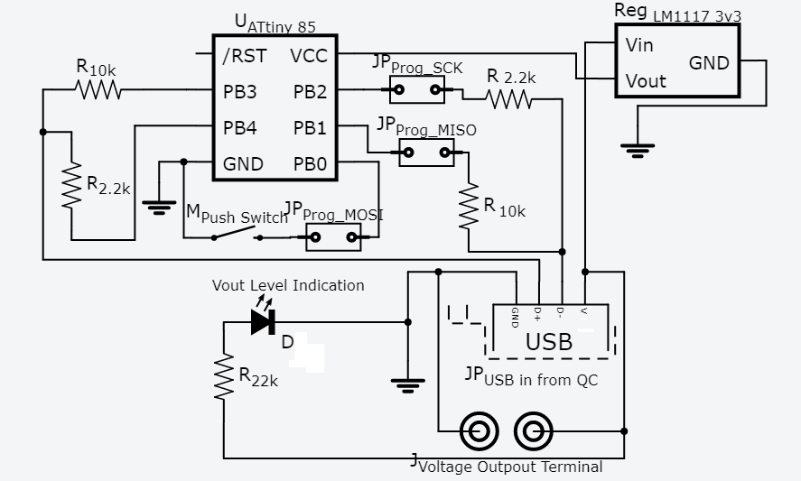
활성 부품은 LM1117 3.3V 레귤레이터와 ATtiny85뿐이며, 나머지는 저항, 스위치, 커넥터, 점퍼, 프로토보드 등 수동 부품입니다. 부품을 깔끔하게 배치 후 납땜하고, 0Ω 점퍼로 내부 연결을 구성합니다.
ISP 프로그래밍 핀(MOSI, MISO, SCK)이 동작 시 GPIO로도 사용되므로, 프로그래밍 시 회로와 격리할 수 있는 점퍼를 배치했습니다.
///========================= Algorithm ========================///
/* First, Connect the D+ pin to a voltage 0.325 to 2 volts and keep the D- floating, then wait at least 2 seconds. Two actions happen during this 2 seconds: The D+ and D- voltage equal a voltage between 0.325 to 2 volts for 1.25 seconds. (because the D+ and D- pins connect together inside the CHY100 at first) Then the D+ keeps at a voltage between 0.325 to 2 volts and the D- voltage decrease to zero. (because the D+ and D- pins disconnect and a resistor inside the CHY100 discharges the D-)*** CHY100 is a QC 2.0 Protocol interface chip inside Power bank/charger ........ other QC 2.0 chips are probably similar Make D+ above 3.0 V first and then connect the D- to a voltage between 0.325 to 2 volts. The VBUS jumps to 9V. While keeping the D- connection with a voltage between 0.325 to 2 volts,make D+ a voltage between 0.325 to 2 volts. The VBUS jumps to 12V. (because the D+ and D- voltage are between 2V and 0.325V) Disconnect the D+ from a voltage between 0.325 to 2 volts . VBUS jumps to 5V, Because the QC2.0 exits Voltage changing mode and VBUS goes to the default value 5V. start from beginning when needing to enter QC2.0 again) */
// ============ IMPORTANT NOTE ================
// *** Sequence of making pins HIGH and LOW is important
// *** If D+ falls below 0.325V during transition because of wrong GPIO Switching Sequence
// *** QC 2.0 will exit High Voltage Mode and VBUS will go back to 5 Volts
// ==============================================
#define PUSH_SWITCH 0
#define Dp_2k2 4
#define Dp_10k 3
#define Dn_2k2 2
#define Dn_10k 1
int Press_Detect = 0;
void setup() {
  pinMode(PUSH_SWITCH, INPUT_PULLUP);
  // Now Initiating QC Handshake by making D+ 0.6 v keeping D- at Gnd
  Init_QC();
}
void loop() {
  //// 5V ////
  while (digitalRead(PUSH_SWITCH) == 1) { }
  delay(250);
  //// 9v ////
  Set_9V();
  while (digitalRead(PUSH_SWITCH) == 1) { }
  delay(250);
  //// 12v ////
  Set_12V();
  while (digitalRead(PUSH_SWITCH) == 1) { }
  delay(250);
  // Set_5V();
}
///********************** Functions **********************///
void Init_QC() {
  //pinMode(Dn_2k2, INPUT);
  //pinMode(Dn_10k, INPUT);
  pinMode(Dp_2k2, OUTPUT);
  pinMode(Dp_10k, OUTPUT);
  digitalWrite(Dp_2k2, LOW);
  digitalWrite(Dp_10k, HIGH);
  delay(3000);
  // now QC protocol is active
}
void Set_9V() {
  pinMode(Dp_2k2, OUTPUT);
  pinMode(Dp_10k, OUTPUT);
  digitalWrite(Dp_10k, HIGH);
  digitalWrite(Dp_2k2, HIGH);
  pinMode(Dn_2k2, OUTPUT);
  pinMode(Dn_10k, OUTPUT);
  digitalWrite(Dn_2k2, LOW);
  digitalWrite(Dn_10k, HIGH);
}
void Set_12V() {
  pinMode(Dp_2k2, OUTPUT);
  pinMode(Dp_10k, OUTPUT);
  pinMode(Dn_2k2, OUTPUT);
  pinMode(Dn_10k, OUTPUT);
  digitalWrite(Dn_2k2, LOW);
  digitalWrite(Dn_10k, HIGH);
  digitalWrite(Dp_10k, HIGH);
  digitalWrite(Dp_2k2, LOW);
}
void Set_5V() {
  pinMode(Dp_2k2, OUTPUT);
  pinMode(Dp_10k, OUTPUT);
  digitalWrite(Dp_10k, HIGH);
  digitalWrite(Dp_2k2, LOW);
  pinMode(Dn_2k2, OUTPUT);
  pinMode(Dn_10k, OUTPUT);
  digitalWrite(Dn_2k2, LOW);
  digitalWrite(Dn_10k, LOW);
}
void Set_20V() {
  // change Voltage Regulator !!!
  // do at your own risk
}