

산업기술

산업 제조
전자 소자는 자동차에서 점점 더 적극적인 역할을 하고 있습니다. 현재 최상위 차량에는 200개 이상의 전자 제어 장치가 포함되어 있으며 그 중 일부는 자동차 조종석에 적용되는 센서 및 프로세서입니다. 자동차용 전자 제품의 가치는 다이내믹 시스템, 차체 및 섀시에 있으며 대부분이 디지털 전원과 관련되어 있다고 결론지을 수 있습니다.
자동차에 전자 시스템을 적용하는 것은 다음 세 가지 측면을 포함하여 자동차 성능을 높이는 것을 목표로 합니다.
a. 환경 개선은 연료 절약, 테일 가스 감소, 가솔린, 천연 가스, 바이오 연료에서 하이브리드 전력 및 순수 전력으로의 연료 변환을 의미합니다. 따라서 전기 자동차는 자동차 산업의 전략적 방향이 되었습니다.
b. 보안 강화는 에어백, 레이더 모니터링, 스테레오 카메라, 적외선 모니터링 및 자동 회피에서 자율 주행에 이르기까지 교통 사고 감소에 있습니다. 현재 자율주행차가 많은 관심과 투자를 받고 있습니다.
c. 편의성과 편안함은 일반적으로 오디오, 비디오 디스플레이, 에어컨, 컴퓨터, 이동 통신, 인터넷, 내비게이션 및 전자 통행료 징수에 뿌리를 두고 있어 편의성과 인간화를 고려합니다.
전자기기의 중추로서 자동차에 적용되는 PCB(인쇄회로기판)도 위와 같은 요건을 충족해야 합니다.
• 품질 보증 요건
제조사나 유통사에 대한 장기적인 품질 보증의 기본 요구 사항은 국제적 관점에서 볼 때 ISO9001인 사운드 품질 관리 시스템에 있습니다. 자동차 산업의 특수성으로 인해 북미의 3대 자동차 제조사가 1994년 자동차 산업에 특화된 품질 경영 시스템인 QS9000을 공동으로 설립했습니다. 21 st 초에 세기에 ISO9001, 즉 ISO/TS16949의 규정을 기반으로 세계 자동차 제조업체에서 새로운 품질 관리 시스템을 발표했습니다.
전 세계 자동차 산업에 대한 기술 규정인 ISO/TS16949는 자동차 산업에 대한 특별 요구 사항을 통합하고 자동차 부품 공급망의 결함 방지, 품질 변동 및 폐기물 감소에 중점을 둡니다.
따라서 자동차 PCB 제조업체가 자동차 시장에 본격적으로 진출하기 전에 획득해야 하는 첫 번째 인증서는 ISO/TS16949입니다.
• 성능에 대한 기본 요구 사항
ㅏ. 높은 신뢰성
자동차의 신뢰성은 크게 두 가지 측면에서 나타납니다. 하나는 제어 장치 및 전자 부품이 정상적으로 작동하는 수명이고 다른 하나는 자동차 제어 장치 및 전자 부품이 극한의 환경에서 훌륭하게 작동하도록 하는 내환경성입니다.
자동차의 평균 수명은 10년에서 12년으로 구성 요소나 취약한 부품만 교체할 수 있습니다. 즉, 전자 시스템과 PCB는 자동차와 같은 서비스 연도를 특징으로 해야 합니다.
차량은 적용 과정에서 영하의 추위, 극심한 더위 및 장기간의 빛과 비에 이르기까지 기후와 환경의 영향을 받는 경향이 있습니다. 그 외에도 전자 부품 및 시스템 작동으로 인해 발생하는 열로 인한 환경 변화를 겪어야 합니다. 자동차 전자 시스템과 PCB도 마찬가지입니다. 자동차 전자 시스템은 온도, 습도, 비, 산성 연기, 진동, 전자파 간섭(EMI) 및 전류 서지를 포함한 환경에서 다음과 같은 가혹함을 극복해야 합니다.
비. 경량화 및 소형화
경량화 및 소형화는 각 부품 및 회로 기판의 경량화 및 소형화로 인한 연료 절감에 유리합니다. 예를 들어, 자동차에 적용되는 ECU(Electronic Control Unit)의 부피는 1,200cm 3 였습니다. 21 st 시작 부분에 100년 동안 적어도 4배는 축소되었습니다. PCB의 경량화 및 소형화는 밀도 향상, 면적 감소, 박형화 및 다중 레이어에서 파생됩니다.
• 여러 유형
기계 및 전자 장치의 조합으로 현대 자동차 기술은 전통적인 기술과 최신 과학 기술을 통합합니다. 다른 부품은 다른 기능을 가진 전자 장치에 따라 다르므로 다른 임무를 가진 PCB의 응용 프로그램으로 이어집니다.
자동차용 PCB는 기판 재질에 따라 무기세라믹계 PCB와 유기수지계 PCB로 구분할 수 있다. 세라믹 기반 PCB의 주요 특성은 높은 내열성과 우수한 치수 안정성으로, 고열 환경의 엔진 시스템에 적용할 수 있습니다. 그럼에도 불구하고 세라믹 기반 PCB는 제조성이 좋지 않아 회로 기판 비용이 많이 듭니다. 최근 개발된 내열성이 향상된 수지 기판의 개발로 대부분의 현대 자동차에는 수지 기반 PCB가 대부분 적용되고 있습니다.
한 가지 일반적인 규칙은 다음과 같습니다. 다양한 성능의 기판 재료를 사용하는 PCB는 다양한 기능의 구현을 담당하는 차량의 다른 섹션에 적용됩니다. 다음 표는 차량 장치 또는 계기의 일부와 호환되는 PCB 유형을 보여줍니다.
| 차량 기기 | PCB 유형 |
| 속도계; 에어컨 | 단일/이중 레이어 PCB 단일/이중 레이어 유연한 PCB |
| 카 스테레오; 모니터 | 이중 레이어 PCB 다층 PCB 유연한 PCB |
| 자동차 통신 장치; 무선 위치 기기; 보안 통제 시스템 | 다층 PCB HDI PCB 유연한 PCB |
| 엔진 시스템; 동력 전달 제어 시스템 | 금속 코어 PCB 리지드 플렉스 PCB |
| 차량 전원 컨트롤러; 탐색 장치 | 내장된 PCB |
• 차량의 다양한 섹션에서 PCB에 대한 신뢰성 요구 사항
자동차는 치안과 관련된 교통수단의 일종으로 신뢰성이 높은 다양한 제품에 속합니다. 역학 및 전자 제품에 대한 일반적인 치수, 외관 및 성능 요구 사항 외에도 신뢰성에 관한 일련의 테스트를 구현해야 합니다.
ㅏ. 열 순환 테스트(TCT)
5개의 레벨은 차량의 다른 섹션에 따라 설정됩니다. 아래 표는 차량의 다양한 섹션에 있는 PCB의 열 순환 온도를 요약한 것입니다.
| 차량 섹션 | 레벨 | 저온 | 고온 |
| 차체 내부 | A | -40°C | 85°C |
| 아래 차량 섀시 | B | -40°C | 125°C |
| 엔진 위 | C | -40°C | 145°C |
| 전송 부품 | D | -40°C | 155°C |
| 엔진 내 | E | -40°C | 165°C |
비. 열충격 시험(TST)
자동차 PCB가 극한의 열 환경에서 적용되는 것은 지극히 정상이며, 이는 외부 열과 자체 본체에서 발생하는 열을 모두 견뎌야 하기 때문에 특히 무거운 구리 PCB의 경우 더욱 어렵습니다. 따라서 자동차 PCB의 내열성에 대한 더 높은 요구 사항이 요구됩니다.
열 충격 테스트에 참여하려면 자동차 PCB를 260°C 또는 288°C의 고온 솔더 페이스트에 10초 동안 3번 담가야 합니다. 그 후 적격 PCB는 적층, 범프 또는 구리 균열과 같은 문제가 없습니다. . 요즘은 납땜 온도가 비교적 높은 PCB 어셈블리에 무연 납땜이 사용되어 열 충격 테스트가 더 필요합니다.
씨. 온도-습도 바이어스(THB) 테스트
자동차 PCB는 비오는 날, 습한 환경 등 수많은 역동적인 환경을 거쳐야 하므로 PCB CAF(Conductive Anodic Filament)의 이동성도 검사할 수 있는 THB 테스트가 필요합니다. CAF는 다음과 같은 상황에서 발생합니다:회로 기판의 인접 비아, 인접 비아 및 와이어, 인접 와이어 및 인접 레이어. 이러한 상황에서 절연성은 감소하거나 지름길로 이어집니다. 절연 저항은 비아, 와이어 및 레이어 사이의 거리에 따라 결정되어야 합니다.
• 고주파 PCB
군용 레이더와 유사하게 근거리 레이더, 자동차 충돌 방지 또는 예측 비상 제동 시스템은 PCB에 의존하여 마이크로파 고주파 신호를 전송합니다. 따라서 일반적으로 PTFE(폴리테트라플루오로에틸렌)를 적용하여 유전 손실이 낮은 기판 재료를 제안합니다. 기질 재료인 일반 FR-4와 달리 PTFE 또는 이와 유사한 고주파 재료는 자연스럽게 독특한 제조성을 요구합니다. 예를 들어, 비아 드릴링 과정에서 특별한 드릴링 속도가 필요합니다.
• 무거운 구리 PCB
차량은 높은 전자 밀도와 전력으로 인해 더 많은 열을 발생시키는 경향이 있습니다. 하이브리드 전력 및 순수 전기 자동차의 수가 증가함에 따라 방열 능력 및 더 큰 전류에 대한 높은 요구를 유발하는 발전된 동력 전달 시스템이 요구됩니다. 이를 위해서는 PCB의 구리 두께를 늘리거나 구리 리드와 금속을 다층 PCB에 내장해야 합니다.
무거운 구리 이중층 PCB를 제조하는 것은 쉬운 반면 무거운 구리 다층 PCB를 제조하는 것은 상당히 어렵습니다. 핵심은 무거운 구리 그래픽 에칭과 무거운 구리 간격 채우기에 있습니다.
무거운 구리 다층 PCB의 내부 회로는 무거운 구리입니다. 이후 그래픽 전사에는 내식성이 매우 높은 두꺼운 필름이 필요합니다. 중동의 우수한 회로를 확보하기 위해서는 식각 시간이 충분히 길어야 하고 식각 장치 및 기술 조건이 최적의 상태를 유지해야 합니다.
내부 도체와 절연체 기판 재료 표면 사이에는 큰 차이가 있으며 일반적인 다층 PCB 스택 업은 수지를 완전히 채우지 못하여 캐비티가 발생하므로 많은 양의 수지를 포함하는 얇은 프리프레그를 제안합니다. 일부 다층 PCB에는 구리 두께가 다른 내부 회로가 포함되어 있어 구별이 큰 영역과 작은 영역에 서로 다른 프리프레그를 사용할 수 있습니다.
• 구성요소 삽입
임베디드 부품 PCB는 조립 밀도를 높이고 제품의 전체 크기를 줄이기 위해 휴대 전화에 처음 적용되었으며 이는 다른 전자 제품에도 본질적으로 중요합니다. 이것이 자동차 전자 장치에 내장 기술이 사용되는 이유입니다.
부품 내장 방식에 따라 다양한 내장형 PCB 제조 옵션이 있습니다.
a. 먼저 홈을 밀링한 다음 웨이브 솔더링 또는 전도성 페이스트를 통해 SMD를 조립합니다.
b. 박막 SMD는 먼저 웨이브 솔더링을 통해 내부 회로에 조립됩니다.
c. 후막 구성 요소는 세라믹 베이스에 인쇄됩니다.
d. SMD는 웨이브 솔더링으로 조립한 후 수지를 패키징에 사용합니다. 이러한 유형의 임베디드 PCB는 높은 신뢰성으로 내열성, 내습성 및 충격 방지와 같은 차량의 요구 사항에 더 적합합니다.
• HDI 기술
엔터테인먼트 및 통신 기능 측면에서 스마트 폰 또는 태블릿 컴퓨터와 유사하게 차량에도 HDI PCB가 필요합니다. 결과적으로 마이크로비아 드릴링, 전기도금 및 상호 연결 기술이 자동차 PCB에 적용되어야 합니다.
• 인덕터 방향
두 개의 인덕터(또는 두 개의 PCB 와이어)가 서로 가까워지면 인덕턴스가 생성됩니다. 한 회로(회로 A)의 전류에 의해 생성된 자기장은 나중에 다른 회로(회로 B)의 전류 구동을 유발합니다. 이 프로세스는 변압기 1차 칼라와 2차 칼라 사이의 상호 효과와 유사합니다. 두 전류가 자기장을 통해 상호 작용할 때 생성된 전압은 상호 인덕턴스(LM ): . In this formula, YB is the error voltage input to Circuit B while LA is the current through Circuit A. LM is quite sensitive to circuit spacing, inductance loop area and loop direction.
Therefore, an optimal method to arrange all inductors in a circuit can be achieved through compact circuit layout and coupling balance reduction.
Distribution of mutual inductance is related with inductance alignment. Therefore, direction modification of Circuit B makes its current loop parallel to magnetic lines of Circuit A. To achieve that, inductors should be vertically arranged, which is beneficial to mutual inductance reduction.
Inductor layout rules for automotive PCBs:
a. Inductor space should be as large as possible;
b. Inductor alignment should be set as right angles so that crosstalk between them will be minimized.
• Lead coupling
Similar with inductor alignment affecting magnetic field coupling, if leads are close to each other, coupling will be affected as well and mutual inductance will be possibly generated. The leading issue in RF circuit lies in sensitive component layout such as input matching network, receiver's resonant channel and emitter's antenna matching network.
Return current path should be as close to main current path as possible with radiation field minimized, which is beneficial to current loop area reduction. Optimal low impedance path is normally grounding area under leads, that is, loop area is effectively limited in the area with dielectric thickness times lead length. If grounding area is split, however, loop area will be enlarged. For leads going across split area, return current will be forced to go across high impedance path, which greatly increases current loop area. This type of layout also makes circuit accessible to mutual inductance.
In a word, integrated grounding should be ensured under leads as much as possible since integrated mass area grounding is beneficial to circuit performance improvement.
• Grounding thru-hole
The main issue RF circuit has to solve usually lies in bad characteristic impedance of circuits, including electronic components and interconnection. Copper layer with low thickness is equivalent to inductance wire. Moreover, distributed capacitance can be formed by the combination between copper layer and adjacent leads. As leads go through thru holes, inductance and capacitance characteristics will be displayed as well.
Thru-hole capacitance mainly derives from capacitance between copper at thru-hole pad edge and bottom copper. Another element affecting thru-hole capacitance is cylinder of metal thru holes. Parasitic capacitance affects little since it usually just leads to low signal edge of high-speed digital signals.
The largest effect of thru holes is corresponding parasitic inductance aroused by interconnection. Because majority of metal thru holes feature the same dimension as that of integrated components in RF PCB design, this formula can be used to estimate the effect of thru hole: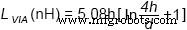 . In this formula, LVIA is the integrated inductance of thru holes; h refers to via height with inch as unit; d refers to via diameter with inch as unit.
As a result, circuit layout should conform to the following principles:
a. Inductance module should be established for thru holes in sensitive area;
b. Filter or matching network depends on independent thru holes;
c. Thinner PCB copper will reduce the effect of thru hole parasitic inductance.
• Grounding and filling
Grounding or power plane defines a public reference voltage that supplies power to all components in the system through low impedance path. Based on that scheme, all the electric fields can be balanced with excellent shielding scheme generated.
Direct current always flows through low impedance path. Similarly, high-frequency current is also a path flowing through the lowest impedance at the first minute. Therefore, for standard PCB leads above ground plane, return current tries to flow into the grounding area rightly under leads. Afterwards, split grounding area arouses all kinds of noises, which further increases crosstalk through magnetic field coupling or current accumulation. As a result, ground integrity should be ensured as much as possible, or return current will drive crosstalk.
In addition, filling ground, also called protective wire, is usually applied for design of circuits containing areas where continuous ground is difficult to be arranged or that requires shielding sensitive circuits. Grounding thru holes can be positioned at terminals of wires or along the wires to increase shielding effect. Protective wires can't be mixed with leads designed to provide return current path, which will bring forward crosstalk.
When copper area isn't connected to ground or connected to ground at one terminal, its validity will be decreased. In some cases, parasitic capacitance will be generated with ambient impedance changed or potential path formed between circuits, which, thus, lead to bad effect. Simply speaking, if copper has to be arranged on the board, the same electroplating thickness should be maintained.
In the end, grounding area near antenna has to be taken into consideration. Any monopole regards grounding area, routing and thru hole as a section of system balance and non-ideal balanced routing will affect radiation efficiency and direction of antenna. Therefore, grounding area mustn't be directly placed right under monopole antenna of a circuit board.
To sum up, the following design principles should be conformed to in terms of grounding and filling:
a. Continuous grounding area with low impedance should be provided as much as possible;
b. Two terminals of filling wires should be connected to the ground with thru hole array applied;
c. Copper-coated lines have to be connected to the ground near circuit around which copper coatings aren't necessary. When it comes to circuit boards with multiple layers, a grounding thru hole should be arranged as signal lines are transferred from one side to the other.
In conclusion, automotive PCB design rules can be summarized into the following table:
| Inductor layout | • Inductor space should be as large as possible; • Inductor alignment should be set as right angles; |
| Integrated grounding | • Integrated grounding should be arranged under leads; |
| Through holes | • Inductance module should be set for thru holes in sensitive area; • Filter or matching network depends on independent thru holes; • Thinner PCB copper reduces the effect of thru hole parasitic inductance; |
| Grounding and filling | • Continuous grounding area with low impedance should be provided; • Connect terminals of filling wires to the ground with thru hole array applied; • Copper-coated lines have to connected to the ground; |
Article wrote by PCBCart editor Dora Yang, first published on Bodo's Power System Magazine August issue, 2017.
You might also be interested in the following articles:
• Properties of Flex-Rigid PCB Used for Automotives
• 5 Tips for Automotive Circuit Design to Defeat EMI
• SMT Soldering Reliability Research Based on Circuit Module in Automotive Electronic Industry
• 5 Proven Ways to Judge Reliability of Automotive PCB Manufacturers
• How to Evaluate an Automotive HDI PCB Manufacturer
산업기술
지그는 구멍을 뚫거나 태핑하는 것과 같은 반복적인 작업을 수행할 때 제조 도구를 제자리에 고정하는 도구입니다. 반면에 고정 장치는 제조 도구를 안내하지 않고 고정된 위치, 방향 또는 위치에서 공작물을 안정적으로 유지합니다. 표준 바이스는 가구의 일반적인 예입니다. 차이점은 제쳐두고, 지그와 고정구 모두 큰 차이를 만드는 도구입니다. 생산성을 높이고 부품의 반복성을 개선하며 부품 조립 및 분해를 더 쉽게 만들고 안전한 작업 환경을 조성하는 데 도움이 됩니다. 거의 모든 자동화된 산업 제조 공정은 제대로 작동하는 부품을 일관되게 제작
2016년 3월 15일 PCB 제조 및 조립 서비스 제공업체는 누군가의 아이디어를 현실로 만드는 막중한 책임이 있습니다. PCB 설계 및 제조 프로세스의 여러 단계에는 다른 파일과 정보가 필요합니다. 따라서 PCB 문서는 클라이언트가 원하는 것을 정확히 제조업체에 전달하는 데 도움이 됩니다. 또한 필요한 정보를 미리 준비하면 전체 처리 시간을 단축할 수 있습니다. 이를 통해 더 쉽고 빠르고 정확한 견적을 얻을 수 있을 뿐만 아니라 오류 없는 PCB 설계 및 제조를 보장합니다. PCB 설계를 위한 중요한 문서 항목 인쇄 회