

산업기술

산업 제조
브레드보드 PCB 프로토타입에서 확장하는 것은 창의성과 절차를 결합한 복잡한 프로세스입니다. 개발 일정은 프로젝트를 실행하는 사람만큼 개별적이며 모든 것은 항상 제작자의 손에 달려 있습니다. 그러나 그 과정에서 찾아야 할 몇 가지 이정표가 있습니다. 브레드보드 PCB
https://youtu.be/HAOvEPh8hms
이제 이 환상적인 아이디어 또는 더 나아가 PoC(개념 증명)를 얻었지만 대량 생산할 가치가 있는 것으로 확장해야 하거나 최소한 데모 목적으로 일부 제조업체에서 제작할 수 있어야 합니다. PCB 프로토타입 제작을 어떻게 시작합니까?
하드웨어 설계에서 PCB 프로토타입은 설계자가 설계를 시각화하고 테스트할 수 있을 만큼 충분히 제조된(쉽게 복제할 수 있는) 제품을 나타내는 "수작업" 모델입니다. 프로토타입이라는 단어는 원본을 의미하는 라틴어 proto와 형태 또는 모델을 의미하는 types에서 유래했습니다.
모든 자습서와 사용 가능한 무료 리소스의 수를 통해 거의 모든 사람이 몇 시간 만에 빠른 PCB 프로토타입을 제작할 수 있게 되었습니다. PCB 프로토타입을 상용화할 수 있는 장소로 가져오는 데는 많은 노력, 계획 및 약간의 전문 지식이 필요합니다. 하드웨어에 대한 많은 결정을 내려야 하며, 이는 결국 장치 소프트웨어에 대한 결정으로 이어집니다. 브레드보드 PCB
Raspberry Pi 또는 인기 있는 Arduino로 빌드하는 것은 쉽지만 이를 사용하여 대량 생산할 수 있는 기회는 대부분 제한적입니다. 물론 이것이 Arduino Pro Mini와 같은 Arduino 보드에 보드를 만들 수 없거나 헤드리스 Arduino가 꽂을 수 있고 그런 다음 계속 제작할 수 있다는 것을 의미하지는 않습니다. 하지만 비용이 많이 들고 필요한 것보다 더 강력할 수도 있습니다.
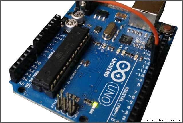
오늘날 많은 하드웨어 스타트업이 Arduino로 첫 번째 PCB 프로토타입을 구축했습니다. . 아두이노 전기 공학 배경이나 필요한 프로그래밍 기술 없이도 배우기 쉽습니다. 어린아이도 할 수 있으며 대부분의 아이들이 할 수 있습니다.
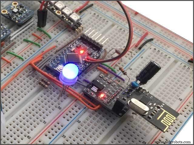
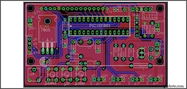
PCB 프로토타입 제작을 시작하는 첫 번째 단계는 필요한 구성 요소를 아는 것입니다. 블록 다이어그램 또는 기존 PoC를 기반으로 아이디어를 빠르게 얻을 수 있으며 원하는 장치 기능조차도 즉시 알 수 있습니다. 예를 들어 착용 가능한 심장 박동 모니터와 같은 것을 구축합니다. 다음 중 일부가 필요합니다.
1. 마이크로컨트롤러 유닛 – Atmega, ARM, PIC 등
2. 맥박 센서 – 전용 맥박 센서가 작동하거나 LED와 광검출기의 조합이 작동할 수도 있습니다.
3. 전원 공급 장치
4. 디스플레이 인터페이스 – LCD, LED, OLED, TFT 등.
단일 전자 공급업체 및 경우에 따라 여러 공급업체로부터 필요한 부품의 전부는 아니더라도 대부분을 쉽게 아웃소싱할 수 있습니다. 다음은 AliExpress, Digi Key, Arrow, Mouser, Adafruit 및 기타 여러 업체에서 세부 정보를 구입할 수 있는 일부 공급업체입니다.
다음 단계는 일반적으로 개략도라고 하는 전자 제품 설계의 다이어그램을 만드는 것입니다. 또는 회로도. 개략도는 모든 구성 요소가 연결되는 방식을 보여줍니다. 이것은 손으로 하는 것이 아니라 이를 위해 설계된 고유한 도구입니다.
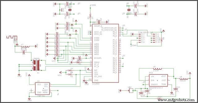
회로도 생성은 최종 장치를 구축하는 핵심 단계이며 건너뛸 여유가 없습니다. 스키마를 시작하는 것은 매우 쉽습니다. 빌드에 적합한 도구를 알아야 합니다. 회로도 설계에는 여러 회로 설계 소프트웨어를 사용할 수 있으며 일부는 무료이며 일부는 유료 버전입니다. 대부분의 설계 소프트웨어는 회로도 그리기 및 PCB 레이아웃 제작에 사용할 수 있습니다.
1. KiCAD – 무료 사용
2. Eagle CAD – 프리미엄이지만 제한된 무료 옵션
3. 알티움 – 프리미엄
4. DipTrace – 프리미엄
5. OrCAD – 프리미엄이지만 무료 평가판을 제공합니다.
사용할 디자인 소프트웨어를 결정한 후에는 소프트웨어마다 모양과 느낌이 다를 수 있으므로 소프트웨어 환경에 익숙해질 수 있습니다.
선택한 소프트웨어에서 회로도를 생성할 때 회로도 설계의 몇 가지 표준 사례를 따라야 합니다.
1. 접합점을 사용하여 접합점에서 연결되는 둘 이상의 연결을 나타냅니다.
2. 수백 개의 연결을 그리는 대신 핀에 네트 이름을 사용합니다. 이렇게 하면 불필요한 혼란 없이 회로도의 가독성이 향상됩니다.
3. 동일한 장치에 대해 항상 동일한 기호 사용
4. 특히 복잡한 회로를 설계할 때 스키마를 논리적 블록으로 분리합니다.
도식 설계를 마치고 완전히 교차 확인했으면 다음 단계는 회로 설계를 PCB 제조로 변환하는 것입니다. 최종 제품의 기능에 부정적인 영향을 미칠 수 있는 레이아웃 오류의 가능성이 높습니다. 여러 PCB 레이아웃이 보드를 제조하는 데 사용됩니다.
다음 장에서는 PCB 프로토타입용 인쇄 회로 기판을 만드는 방법에 대해 설명합니다.
PCB 프로토타입용 인쇄 회로 기판 만들기 먼저 회로도를 만드는 것은 본격적인 전문 기판을 만드는 과정의 한 단계입니다.
건너뛸 수 없는 프로세스의 다음 단계는 인쇄 회로 기판의 레이아웃을 설계하는 것입니다. 그러나 인쇄 회로 기판이란 무엇입니까?
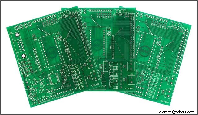

인쇄 회로 기판 , PCB라고도 하는 모든 전자 부품을 한 곳에 보관하고 연결하는 물리적 보드입니다. 회로도 설계는 일반적으로 여러 방법을 사용하여 PCB로 전송됩니다. PCB의 설계는 다음과 같은 몇 가지 요인에 영향을 미칩니다.
1. 비용 – 보드가 중요할수록 만드는 비용이 더 많이 듭니다.
2. 성능 - 보드 디자인과 사용된 구성 요소 유형은 기기의 전체 성능에 영향을 미칩니다. 잘못 설계된 보드는 노이즈에 취약하여 기기의 성능을 저하시킬 수 있습니다.
3. 내구성,
4. 그리고 더 많습니다.
PCB는 회로도 생성에 사용된 것과 동일한 소프트웨어로 설계되었습니다.
소프트웨어는 주어진 구성 요소와 개략도를 기반으로 PCB 레이아웃과 풋프린트를 생성하는 역할을 합니다. 회로도가 없으면 소프트웨어는 기본 PCB 레이아웃을 생성하지 않습니다.
PCB 레이아웃 제작을 시작하는 것은 처음 사용자에게 시간이 많이 걸리고 지루할 수 있습니다. 그래도 다행스럽게도 대부분의 PCB 소프트웨어를 구축하는 방법을 배울 수 있는 몇 가지 편리한 자습서와 리소스가 온라인에 있습니다.
선택한 소프트웨어에 따라 일반적으로 사용자가 회로도 보기에서 PCB가 설계될 PCB 레이아웃 보기로 전환하는 방법이 있습니다.
최종 장치 모델을 구상할 때 PCB를 설계하십시오. 또한 사용 중인 소프트웨어에는 PCB 레이아웃이 사용된 PCB 프로세스에 대한 설계 규칙을 충족하고 PCB가 회로도와 일치하는지 확인하기 위한 다양한 검증 도구가 있습니다. 디자인이 기기를 망가뜨릴지 여부를 빠르게 테스트할 수 있습니다.
제품이 작을수록 구성 요소가 더 조밀할수록 함께 포장해야 하는 PCB 레이아웃을 만드는 데 시간이 더 오래 걸립니다. 제품이 많은 양의 전력을 라우팅하거나 무선 연결을 제공하는 경우 PCB 레이아웃이 훨씬 더 중요하고 시간이 많이 걸립니다.
대부분의 PCB 프로토타입 디자인의 필수 부품은 전원 라우팅, 고속 신호(크리스탈 클럭 등) 및 무선 회로입니다.
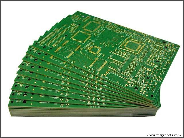
PCB 프로토타입 설계를 보완한 후 인쇄 회로 기판 제조로 이동해야 하며 이를 수행하는 몇 가지 방법이 있습니다. 집에서 직접 만들거나 PCB 제작 전문 제조업체에 디자인을 보내십시오.
집에서 PCB를 생산하는 기술이 있지만 단순한 디자인에 국한됩니다. 따라서 PCB 프로토타입 생산을 아웃소싱해야 할 가능성이 큽니다.
다음 장에서는 타사 제조업체에서 인쇄 회로 기판을 제조하는 방법에 대해 설명합니다.
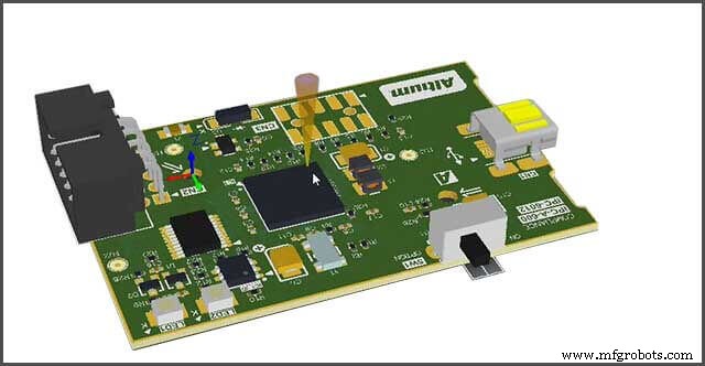
기기의 인쇄 회로 레이아웃을 성공적으로 개발했으면 다음으로 기판을 만들어야 합니다. 제조를 시작하기 전에 최종 제품이 어떻게 보일지 항상 확인하는 것이 좋습니다. Proteus 또는 Altium과 같은 일부 소프트웨어에는 3D 레이아웃 뷰어가 있어 보드를 3D로 보고 보드가 어떻게 보이는지 느낄 수 있습니다.
제조할 디자인을 보내기 전에 먼저 제조업체에서 사용할 파일 형식을 생성하고 사용할 파일 형식을 결정해야 합니다. WellPCB는 제조 분야의 리더입니다.
PCB 설계는 대부분의 전문가가 사용하는 PCB 산업 표준인 Gerber 파일로 변환되어야 합니다. Gerber 파일에는 PCB 생산에 필요한 모든 설계 파일이 포함되어 있습니다. WellPCB는 4가지 파일 형식(Gerber, pcb, pcbdoc 또는 cam 파일 형식)을 허용합니다.
WellPCB는 양면에 실크스크린을 인쇄하며 추가 비용 없이 제공됩니다. 인쇄된 실크스크린 레이어에 부품 번호를 포함하는 것이 좋습니다. 보드 하우스 사양을 아는 것도 좋은 생각입니다. WellPCB는 라인/트랙 폭과 공간에 대해 최소 3mil을 가지고 있습니다. 당신의 디자인이 그것을 초과하지 않는지 확인하십시오. 소프트웨어 설계 규칙 검사를 사용하여 보드가 제조업체의 생산 능력을 초과하지 않는지 확인하십시오.
실크스크린 요구 사항에는 PCB의 원하는 색상이 명시되어 있으며 대부분은 UV 경화 잉크이며 RoHS를 준수합니다.
1. 흰색
2. 노란색
3. 블랙
가장 널리 사용되는 색상입니다. 다른 제품도 사용할 수 있으며 색상이 처리 시간과 비용에 추가될 수 있습니다.
4. WellPCB PCB 온라인 견적 섹션 방문 – https://www.wellpcb.com/pcb-quote
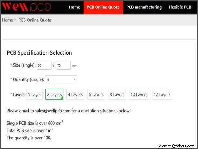
5. 보드 세부 정보를 입력하고 장바구니에 추가를 클릭합니다. 맞춤형 PCB 회로 기판을 온라인으로 주문하는 방법에 대해 알아야 합니다. 필요한 PCB 보드의 경우 WellPCB로 문의할 수 있습니다. 최소 수량은 5개 단위입니다.Breadboard PCB
6. 새 계정을 등록합니다.
7. PCB Gerber를 업로드하거나. Brd 파일.
8. 상품을 주문하고 배송될 때까지 기다리세요.
WellPCB는 또한 모든 클라이언트 파일의 전체 DRC 검사를 수행하는 데 도움이 됩니다. 이는 특히 설계에 문제나 오류가 있는 경우에 유용합니다. 사용자는 보드 제작 중 시간과 비용을 낭비하지 않도록 문제에 대해 경고를 받습니다.
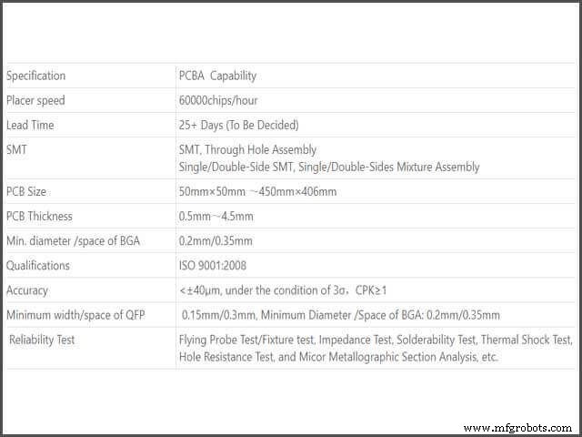
이제 앉아서 인쇄 회로 기판이 도착하기를 기다립니다. PCB 서비스를 위한 PCB 제작 리드 타임은 8 – 12 레이어 PCB의 경우 최소 24시간, 최소 약 120시간입니다.
다음 장에서는 PCB 용어와 WELLPCB 기능에 대해 이야기하겠습니다.
WellPCB는 인쇄 회로 기판의 선두 제조업체이며 PCB 프로토타입과 함께 인쇄 회로 기판 어셈블리를 제공합니다.
This makes WellPCB your go-to manufacturer for your entire product development. Also, they provide Turnkey services for outsourcing the components for your electronic board. Breadboard PCB
WellPCB is focused on offering PCB prototypes services and not just large-scale manufacturing. Their PCB prototypes services go at a minimum of 5 units. Not only are they offering prototyping services but also packaged at some meager prices.
A promotional price of $3.99 for users looking for 1-2 layers, 10pcs PCB prototypes, and a board of less than 10cm*10cm.
WELLPCB is capable of producing 100,000 square feet of 2-32-layer PCBs and delivering over 5000 varieties monthly.
With a quick turn to meet 24-hour delivery for double-sided PCBs, 48-hour for 4 to 8 layers, and 120-hour for ten layers or higher PCBs. Their standard lead time is about 5 – 6 days and an Expedited time of 24 – 48 hours.
1. Support Material:FR4, High TG FR4, Halogen Free material, CEM-3, Rogers HF material.
2. Layer counts 1-32 layers.
3. Finished Copper Thickness:0.5-5 oz.
4. Finished Board Thickness:0.2-6.0mm.
5. Min. Line/Track Width:4mil.
6. Min. Line/Track Space:4mil.
7. Min. Contour Tolerance:+/-0.1mm.
8. Min. Finished Diameter of PTH Hole:0.1mm.
9. Max. Board Thickness/Hole Ratio:12:1.
10. Min. Solder Mask Bridge:4mil (Min. SMT Pad Space 8mil).
11. Min. Legend(Silkscreen) Track Width:5mil.
12. Solder mask color:green, black, blue, white, yellow, matt, etc.
13. Solder mask hardness:6H.
14. Legend/Silkscreen Color:white, yellow, black, etc.
15. Surface Treatment:HAL, Lead-Free HAL, Immersion gold, OSP, Immersion Tin, Immersion silver, etc.
16. Other Technology:Gold finger, peelable mask, Non-across blinded vias, characteristic impedance control, Rigid-flex board, etc.
17. Reliability Test:flying probe test/fixture test, impedance test, solderability test, thermal shock test, hole resistance test.
18. Flammability:94V-0.
A PCB surface finish is a coating between a component and a bare board PCB. It is applied for two primary reasons:to ensure solderability and to protect the exposed copper circuitry.
Standard surface finishes preference – Non-RoHS or RoHS compliant.
1. HASL (Hot Air Solder Level) – Contains Lead non-RoHS, cheaper and quite popular.
2. ENIG (Electroless Nickel Immersion Gold) – Most popular finish and lead-free, but expensive
3. Immersion Silver – RoHS compliant will tarnish like any silver product
4. OSP – Organic Solderability Preservative
5. LF-HASL (Lead-Free Hot Air Solder Level)
6. Immersion Tin – Used the least of all finishes
Soldermask is the color to be used for the PCB prototypes finish. Any color can be used. However, sticking to standard colors is the best and more professional. The most popular are:
1. Green
2. Blue
3. Black
4. Red
5. White
6. Yellow
Mask can be in either Matte or Gloss in those above colors. Matte is less readily available due to Gloss is most widely used. Processing Matte for specific colors may add time due to equipment change and processing cleans up and application.
Silkscreen is the printing done on the PCB for identification. It is used on the component side to identify components, test points, PCBA part numbers, warning symbols, company logos, and manufacturer names. The following are some of the colors being used:
1. Black
2. White
3. Yellow
Those are the most widely used colors; others are available; however, colors can add to process time and cost like MASK. Ask if you have special requirements for your product.
In the next chapter, we will talk about how to move your PCBA mode.
So, what’s PCB Rapid Prototyping. PCB assembly. Directly speaking, PCB Rapid Prototyping. PCB assembly. Directly speaking, PCB Rapid Prototyping. 3D PCB Printing makes the PCB and does the Printed Circuit Board Assembly (PCBA, an abbreviation for printed circuit board assembly, which refers to the combination of PCB prototypes manufacture, components sourcing, and B3D PCB Printing makes the PCB and does the Printed Circuit Board Assembly PCBA is the PCB with components assembled).
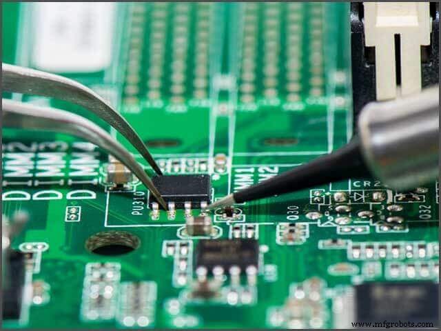
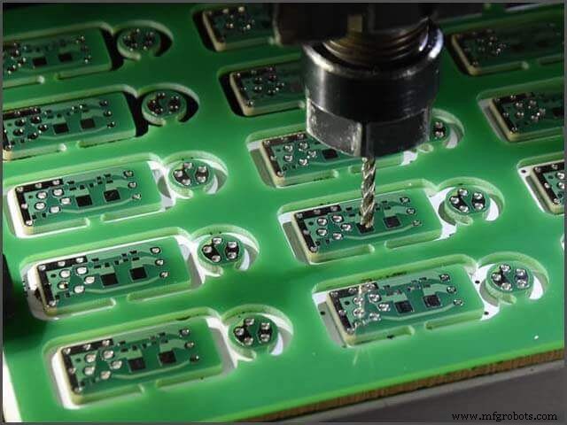
So now you have your printed circuit board available and ready to populate the board with the needed components. You might be tempted to solder this manually yourself. This might be a good option, especially when the number of panels is less than five or, worst case, ten units; anything more than that might not be a good idea but going the route of PCB Rapid Prototyping. 3D PCB Printing not only makes the PCB but also does the Printed Circuit Board Assembly PCBA.
The main assembly types of PCBA are shown below:
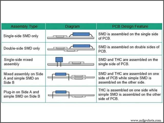
Those are the commonly used PCB Rapid Prototyping. 3D PCB Printing makes the PCB and does the Printed Circuit Board Assembly (PCBA assembly types. SMD means Surface Mount Devices, and THC implies Through Hole Components).
It is usually faster and cheaper on bulk orders. Getting started with PCB Rapid Prototyping. 3D PCB Printing makes the PCB, and does the Printed Circuit Board Assembly (PCBA is also relatively simple as far you have the necessary resources).
Just like, WellPCB is capable of handling all your possible PCB prototypes works, they also offer an accompanying production film work that you require to manufacture PCBs. In the case of PCBA service to help one streamline the whole board development process. It does not cost much more to have the PCB populated unless you tack on additional steps in the process, such as burning a program to the MCU or running 100% test on the finished boards.
To get started with PCBA, you need to have all the required documents.
Aside from your PCB prototypes design file, you will need a design specification if there are special needs for your work, a bill of the material (BoM) list for the number of components on your board and also can be generated from the software being used, and part placements made from the software used.
The board owner can decide to source for the parts alone and send them to WELLPCB for assembly or let WellPCB handle the integral components sourcing, which I feel is better. Of course, partial supply can also be agreed upon.
Go to PCB Assembly on WellPCB here and fill the Request for Quotation (RFQ) form. Input as many details as possible and send it. WellPCB will get in touch if they need more information from you and continue the assembly process order.
The WellPCB Bill Of Materials (BOM) of a PCB gets fitted onto aboard. PCB Assembly process can take up to around 25 days for large volume manufacturing, which is an excellent time for large volume PCB assembly compared to other PCB Assembly manufacturers. This will make it easy for a pick and place machine to easily pick and place the components on the PCB Assembly capabilities:
More information about WellPCB SMT). This will make it easy for a pick and place machine to easily pick and place the components on the PCB Assembly capability can be found here.
At this point, all you have to do is to sit down and wait for your populated PCB to be available and sent to you. This concludes the end of this chapter, and the next chapter will discuss how to save money when doing PCB and PCBA.
Now congratulation, you have your fully developed hardware PCB prototypes or, better still, hardware board. For newbies, this will have been a good experience, and also a lot of money must have been sent which could have been avoided.
Some of the money spent could have been avoided due to unnecessary complexity and errors in the PCB and circuit design.
This chapter will show some of the handy tips and tricks that can help you save even millions when doing large volume manufacturing.
Keeping your board size at a minimum is crucial in saving costs and making your final product as portable as possible. The bigger it gets, so do the prices. If the board becomes smaller, so does the cost.
Also, making your board too small might not save you cost since assembling and preparing your board might require specialized equipment.
You might be tempted to use DIP (dual in-line) package, commonly known as Through-hole components, because it’s possible to easy to use but might not be the best cost-saving option.
1. Using surface mount components will reduce the number of holes that need to be drilled on your board typically used for through-hole parts.
2. Using surface mount components will also reduce the board size.
3. Using surface mount components will make the board assembly faster and lesser equipment used.
By going on board penalization, you can save yourself a ton of money. Getting all of your boards on one panel means that a rapid-fire pick and place machine can get all your parts placed in one go without requiring any additional setup time.
Requesting silk screening on one side will cut your artwork costs in half. Sticking with standard colors and larger geometries will also prove beneficial. Understanding these constraints can help you to better PCB prototypes pricing and cost savings.
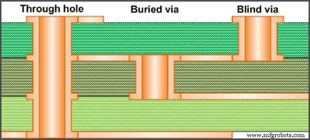
There are three types of vias – through-hole vias, blind vias, and buried vias. The last two are only going to be used for high-density and high-frequency PCBs. So, this one is simple, if your design doesn’t need these types of vias, leave them out to avoid any extra manufacturing costs.
This concludes the end of this chapter and the end of this guide. Using standard materials and several of these tips mentioned above can save you several thousand to millions of dollars when embarking on large volume manufacturing.
When building and launching your products to market, some other things also need to be considered.
1. Certifications – Every wireless-based product needs to go through some certification process to be clear of any hazards or issues and be permitted to the market.
2. Enclosure – Depending on the type of product you are building, you might need some enclosure around your board to give it some artistic look or for some reason.
3. Quality Control – Quality control issues a formal inspection report for review and shipment approval. You should expect each shipment to be inspected and approved before being released. Such a protocol creates a closed-loop process that builds in continuous improvement for consecutive production runs.
This guide should give you enough head start in launching your following product. Taking an idea from concept to production is not for the faint of heart.
You have to withstand failures, criticism, mishaps, and managing the whole manufacture process can be very challenging. Still, a manufacturer like WellPCB is in the business to help you succeed. Breadboard PCB
산업기술
의심할 여지 없이 대부분의 일반 엔지니어링 프로젝트는 표준 PCB 설계를 사용합니다. 또한 기존 PCB가 모든 작업에 작동할 수는 없습니다. 따라서 고급 응용 프로그램을 처리하는 경우 고속 PCB가 필요합니다. 그러나 고속 PCB를 설계하는 것은 까다로울 수 있습니다. 신호 무결성, 반사 및 누화와 같은 세부 사항에 주의를 기울여야 합니다. 이러한 용어에 익숙하지 않은 경우 이 도움말을 참조하세요. 이 기사에서는 고속 PCB와 설계 규칙에 대한 모든 것을 배울 것입니다. 고주파 PCB와도 비교하겠습니다. 자, 시작하겠습니다.
PCB라고도 하는 인쇄 회로 기판은 오늘날 모든 전자 부품의 핵심을 형성합니다. 이 작은 친환경 부품은 일상적인 가전제품과 산업 기계 모두에 필수적입니다. PCB 설계 및 레이아웃은 모든 제품 기능의 중요한 구성 요소입니다. 이것이 장비의 성공 또는 실패를 결정합니다. 기술의 끊임없는 진화와 함께 이러한 디자인은 계속해서 발전해 왔습니다. 오늘날 이러한 설계의 복잡성과 기대치는 전기 엔지니어의 혁신 덕분에 새로운 수준에 도달했습니다. 최근 PCB 설계 시스템 및 기술의 발전은 업계 전반에 걸쳐 광범위한 영향을 미쳤습니다. 결과적