

나노물질

산업 제조
단결정 구리의 나노 절단 공정에서 재료 제거 및 표면 아래 결함 발생에 대한 유체 매체의 영향은 분자 역학 시뮬레이션을 통해 조사되었습니다. 본 논문에서는 수성 매질을 사용하여 나노 절단 공정 중 공작물의 원자 이동 및 전위 전개를 분석하여 칩의 제거 메커니즘 및 가공 표면의 형성 메커니즘을 조사하였다. 온도 분포와 표면 아래 결함 결정 구조 변형을 조사하며, 이는 중심 대칭 매개변수와 공통 이웃 분석 방법으로 분석됩니다. 결과는 절삭 공구의 압출 전단 작용에 의해 공작물 재료가 제거됨을 보여줍니다. 수성 매체의 윤활은 절삭력을 감소시키고 절삭 칩의 높이를 낮출 수 있습니다. 특히, 유체 매체의 냉각 작용으로 인해 공작물의 표면 아래에 "입자 경계와 유사한" 전형적인 결함이 형성됩니다. 그리고 유체 매체를 사용하여 나노 절단 공정에서 공작물의 온도가 현저히 감소합니다.
<섹션 데이터-제목="배경">다이아몬드 절단은 서브미크론 치수 정확도와 나노미터 표면 마감을 가진 나노 구조 표면을 생성하는 효과적인 기술로 널리 간주됩니다[1]. 나노 스케일에서 재료 제거 및 가공 표면 형성 메커니즘은 나노 절단 공정에서 가공 정확도 향상에 중요합니다. 초기 연구에서 연구자들은 재료의 변형[2,3,4], 표면 결함 진화[5,6,7], 잔류 응력[8,9], 결정 상전이[10, 11] 진공 환경에서 나노 절단 공정 중. 그러나 실제 금속재료의 나노미터 절단에서 냉각 및 윤활유의 역할은 가공 성능 향상에 매우 중요하다[12]. 따라서 나노 절단 공정에서 재료 제거 및 표면 아래 결함 발생 메커니즘에 대한 유체 매체의 영향에 대한 연구가 필요합니다.
최근 몇 년 동안 나노 절단 공정의 가공 메커니즘은 분자 역학(molecular dynamics, MD) 시뮬레이션에 의해 널리 연구되고 있으며, 이는 나노미터 절단 공정을 연구하는 효과적인 방법임이 입증되었습니다. 예를 들어, 표면 생성 및 나노 절단에서 상 변형에 대한 회복 및 측면 유동의 영향은 Fang[13]에 의해 연구되었습니다. 그리고 사이드 플로우의 억제는 나노 절단에서 발생하는 표면 거칠기를 개선하는 효과적인 방법임을 발견했습니다. Urbassek[14]는 나노결정질 금속의 긁힘을 연구하기 위해 MD 시뮬레이션을 채택했으며 결정립 방향이 더미 모양에 지배적인 영향을 미치고 마찰 계수에도 강하게 영향을 미친다는 것을 발견했습니다. Sharma [15]는 나노 스케일 절단에서 재료 변형 메커니즘, 표면 아래 결함, 절단력, 특정 절단 에너지, 쟁기 효과 및 표면 거칠기에 대한 6가지 다른 결정 방향의 영향을 조사했습니다. Luo[16]는 나노구조의 스케일업 제조를 위한 다이아몬드 선삭에서 나노스케일 멀티팁 다이아몬드 도구를 사용하여 형상 전달성을 입증했습니다.
절삭 방향, 절삭 깊이, 절삭 속도 및 공구 형상과 같은 절삭 매개변수를 합리적으로 선택하여 나노 부품의 표면 아래 결함 형성 및 표면 거칠기를 억제할 수 있습니다. 그러나, 표면결함의 형성을 억제하고 발생기구에 의한 표면품질을 향상시키는 데에는 성공할 수 없다. 또한, 이러한 연구는 진공 환경에서 나노 절단 공정에 초점을 맞추고 있습니다. 실제로 나노미터 절단에서는 공구와 공작물 사이에 대기 및 냉각 액체 매체가 존재하여 나노 절단 메커니즘과 나노구조물의 표면 품질에 영향을 미칠 수 있습니다.
이상의 고찰을 바탕으로 많은 학자들이 유체매체를 이용한 나노가공공정에 대한 연구를 수행하였다. 예를 들어, Mylvaganam [17]은 O2의 효과를 조사했습니다. MD 시뮬레이션을 사용하여 다이아몬드 큐빅 실리콘의 나노 압입에 대해 O2 분자는 산소 원자로 해리되어 실리콘 원자와 화학 결합을 형성합니다. Rentsch[18]는 절삭유가 응력과 온도 분포에 큰 영향을 미친다는 사실을 발견하고 절삭유가 공구 마모를 줄일 수 있다고 지적했습니다. Liu[19]는 나노 절단에서 표면 품질과 도구 마모에 대한 대기 분자의 영향을 연구했습니다. 결과는 대기 분자의 윤활로 인해 절삭력이 감소하고 공구 마모가 감소함을 나타냅니다. Singh[20]은 금속 제거 공정에 대한 나노 입자 절단 유체의 영향을 연구했습니다. Wang[21]은 나노 압입 공정에서 물 분자가 마찰 거동 및 특성 측정에 미치는 영향을 논의했으며 물 분자의 참여가 초기 압입력을 증가시키고 가장 큰 압입력을 감소시킨다는 것을 발견했습니다. Chavoshi[22]는 환원된 산소 조건에서 단결정 실리콘의 고온 나노스크래칭을 연구했으며 시뮬레이션에서 고압 실리콘 상의 잔류물이 관찰되지 않았습니다.
가용한 문헌에서 유체 매체를 이용한 나노 절단 공정에 대한 선행 연구는 도구 칩 인터페이스 영역에 위치한 소수의 분자 또는 나노 입자의 시뮬레이션 모델을 기반으로 합니다. 그러나 다른 영역에서는 유체 매체가 추가되지 않고 유체 매체의 윤활이 제한적으로 분석됩니다. 모델의 유체 매체가 충분하지 않기 때문에 유체 매체의 냉각 작용은 나노 절단 공정에 영향을 미치지 않는 반면 유체 매체의 냉각 작용은 윤활 작용만큼 가공 정확도 및 표면 품질에 중요합니다.
따라서 본 논문에서는 절삭유체에 의해 절삭공구와 가공물이 완전히 둘러싸이게 되는데, 절삭유체는 Tool-Chip Interface의 작용영역 뿐만 아니라 공작물 표면, 가공면, 후면 영역에도 존재한다. 도구의. 따라서 절삭 공구와 공작물 사이의 유체 매체의 적절한 윤활을 조사할 수 있습니다. 또한, 유체 매체는 나노 절단 과정에서 일정한 온도로 설정되며, 유체 매체의 냉각 작용도 잘 연구할 수 있습니다. 수성 절삭유는 물 뿐만 아니라 수용성 기유, 피마자유, 트리에탄올아민, 붕산, 계면활성제, 폴리에틸렌글리콜, 인산나트륨 등을 포함하는 초정밀 가공공정에 널리 사용됩니다. 그럼에도 불구하고 절삭유의 주성분은 수성 매체이며 절삭유에서 수분의 질량 분율은 약 70%에 달한다. 다른 모든 물질의 MD 모델을 구축하는 데 어려움이 있고 잠재적인 기능 매개변수가 알려지지 않았기 때문에 수성 절삭유를 사용한 나노 절삭에 대한 연구는 분자 역학 전산 시뮬레이션 방법으로 수행할 수 없습니다. 따라서 본 연구에서는 나노 절단 공정 시뮬레이션에서 수성 절삭유를 대체하기 위해 절삭유의 주성분인 수성 매체를 사용하였다. 확립된 MD 모델을 기반으로 나노 절단 공정을 수행하여 물 매체가 재료 제거 및 표면 결함 형성 메커니즘에 미치는 영향을 연구합니다. CSP(centro-symmetry parameter), CNA(Common Neighbor Analysis), DXA(Dislocation Extract Algorithm) 방법을 사용하여 표면 아래 결함 전개, 절삭력 변화, 가공물의 온도 분포 및 표면 결함 결정 변형을 조사합니다. .
유체 매체가 나노 절단에서 재료 제거 및 표면 아래 결함 발생에 미치는 영향을 조사하기 위해 그림 1과 같이 수성 매체가 있거나 없는 MD 모델이 설정되었습니다. 모델에서 물 분자는 다음과 같이 구성됩니다. TIP4P 모델 [23,24,25]. CHARMM force field 및 Lennard-Jones(L-J) 전위 함수는 물 분자의 움직임을 정확하게 계산하는 데 사용됩니다. 비결합 위치 에너지, 결합 팽창 전위, 결합 각도의 굽힘 위치 에너지 및 분자 진동의 영향을 종합적으로 분석할 수 있어 물 분자의 시뮬레이션이 보다 정확해집니다. 공작물 재료는 단결정 구리이고 가공 도구는 다이아몬드 재료입니다. 그것은 62835개의 물 분자, 368208개의 Cu 원자 및 2452개의 C 원자를 포함합니다. 공작물은 뉴턴 층, 온도 층 및 경계 층의 세 부분으로 나뉩니다. 크기 효과를 줄이기 위해 [001]과 [010]에서 주기적인 경계 조건(PBC)을 채택하였다. 수중 매체의 압력과 밀도를 유지하기 위해 [001] 방향의 양쪽에 반사벽이 사용됩니다. 실제 가공공정에서는 절삭열의 대부분을 절삭유가 발산하므로 본 작업에서는 수온을 300K로 일정하게 설정하였다. 진공 환경의 MD 시뮬레이션 모델은 그림 1b에 나와 있으며 초기 시뮬레이션 조건은 유체 환경 모델과 유사합니다. 두 모델 사이의 다른 설정은 수성 매체에 대한 관련 설정입니다. 자세한 절단 매개변수는 표 1에 나와 있습니다.
<그림>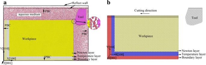
나노 절단의 MD 시뮬레이션 모델. 아 수성 매체의 사용. ㄴ 진공 환경 사용
MD 시뮬레이션에서 잠재적 기능은 시뮬레이션 결과에서 결정적인 역할을 합니다. 재료 특성은 기본적으로 원자 간의 상호 작용에 의해 제어됩니다. 이 연구에서 모델은 공작물, 절삭 공구 및 수성 매체의 세 부분으로 나뉘며 Cu, C, H 및 O 원자의 4가지 원자 유형을 포함합니다. 서로 다른 원자 간의 상호 작용은 Morse 전위, EAM(embedded-atom method) 전위, Lennard-Jones(L-J) 전위 및 Tersoff 전위로 계산됩니다. 서로 다른 원자 사이의 선택된 전위 함수에 대한 자세한 소개는 표 2와 같습니다.
공작물의 Cu 원자와 절삭 공구의 C 원자 사이의 상호 작용은 Eq와 같이 모스 전위에 의해 계산됩니다. (1) [26].
$$ u\left({r}_{ij}\right)=D\left[\exp \left(-2\alpha\left({r}_{ij}-{r}_0\right)\right )-2\exp \left(-\alpha \left({r}_{ij}-{r}_0\right)\right)\right] $$ (1)여기서 r 0 , α , 및 D 는 각각 원자간격, 탄성계수, 결합에너지이다. r의 값 0 , α , 및 D 표 3에 나와 있습니다.
공작물에 있는 Cu 원자 사이의 원자간 기능은 EQ로 표시되는 EAM 전위로 설명됩니다. (2) 및 (3) [27, 28].
$$ E\kern0.5em =\kern0.5em \sum \limits_i^N\left[F\left({\rho}_i\right)\kern0.5em +\kern0.5em \sum \limits_{j\kern0 .5em>\kern0.5em i}^Nu\left({r}_{ij}\right)\right] $$ (2) $$ {\rho}_i\kern0.5em =\kern0.5em \sum \limits_jf\left({r}_{ij}\right) $$ (3)Lennard-Jones 전위 함수는 원자 사이의 장거리 쿨롱 힘과 단거리 반 데르 발스 힘의 상호 작용을 포함하는 이중 전위입니다. L-J 전위는 종종 액체 재료를 시뮬레이션하는 데 사용됩니다. 이 논문에서 Lennard-Jones 전위는 물 분자와 다른 원자 사이의 상호 작용을 계산하는 데 사용되며 이는 Eq. (4) [29].
$$ {U}_{LJ}(r)\kern0.5em =\kern0.5em 4\varepsilon \left[{\left(\frac{\sigma }{r}\right)}^{12}\kern0 .5em -\kern0.5em {\left(\frac{\sigma }{r}\right)}^6\right] $$ (4)여기서 σ 상호 작용 위치 에너지가 0이고 ε일 때 평형 분리입니다. 위치 에너지 트랩의 깊이입니다.
다른 재료의 경우 σ 그리고 ε 식으로 계산할 수 있습니다. (5) 및 (6) [29].
$$ {\sigma}_{\alpha \beta}\kern0.5em =\kern0.5em \frac{\sigma_{\alpha \alpha}\kern0.5em +\kern0.5em {\sigma}_{\beta \베타}}{2} $$ (5) $$ {\varepsilon}_{\alpha \beta}\kern0.5em =\kern0.5em \sqrt{\varepsilon_{\alpha \alpha}\cdot {\varepsilon }_{\베타 \베타}} $$ (6)이 연구에 사용된 원자간 L-J 전위 매개변수는 표 4에 나열되어 있습니다.
다이아몬드 공구의 탄소 원자 사이의 상호 작용은 Eq로 표시되는 Tersoff 전위에 의해 계산됩니다. (7) 및 (8) [30].
$$ E\kern0.5em =\kern0.5em \frac{1}{2}\sum \limits_{i\ne j}{V}_{ij} $$ (7) $$ {V}_{ij }\kern0.5em =\kern0.5em {f}_c\left({r}_{ij}\right)\left[{V}_R^{\hbox{'}}\left({r}_{ ij}\right)\kern0.5em +\kern0.5em {b}_{ij}{V}_A\left({r}_{ij}\right)\right] $$ (8)여기서 f ㄷ (r 이 )는 원자 사이의 절단 함수, V A (r 이 )은 이중 포텐셜 흡수 항, V R (r 이 )는 반발 항의 이중 잠재력이며, r 이 원자 i 사이의 원자 거리입니다. 및 원자 j .
단결정 구리의 나노 절단에서 변형 및 전위는 공작물의 표면 아래에서 핵이 생성됩니다. 이 논문에서는 중심 대칭 매개변수(CSP)를 도입하여 공작물의 전위 핵 생성 및 결함 전개를 분석합니다. FCC(Face Center Cubic) 재료의 경우 CSP 값은 Eq. (9) [31].
$$ CSP\kern0.5em =\kern0.5em \sum \limits_{i\kern0.5em =\kern0.5em 1}^6{\left|{R}_i\kern0.5em +\kern0.5em {R }_{i+6}\right|}^2 $$ (9)여기서 R 나 는 동일한 거리에 있는 인접 원자이고 R i + 6 는 반대 방향의 이웃 원자입니다. FCC 결정, 부분 전위, 적층 결함 및 표면 원자의 CSP 값은 각각 0, 2.1, 8.3 및 24.9입니다[32]. 대표적인 결정구조와 원자색에 대한 CSP값의 범위는 Table 5와 같다.
CSP 방법은 원자 구성을 식별할 수 있지만 공작물의 국부적인 원자 결정 구조 상태를 인식할 수 없습니다. 따라서 CNA(Common Neighbor Analysis)가 도입되어 공작물의 국부적 결정 구조를 식별합니다. Honeycutt[33]이 제안한 독창적인 CNA 방법에서는 다양한 구조를 도표로 표현하였다. 현재 OVITO 소프트웨어[34, 35]에서 각각 FCC(Face Center Cubic), HCP(Closed-Packed hexagonal), BCC(Body centered Cubic), 20면체의 5가지 구조를 빠르게 식별하도록 개선되었습니다[34, 35]. (ICO), 알 수 없음. 이 논문에서는 전위 결함의 전개를 분석하기 위해 전위 추출 알고리즘(DXA)[36]도 소개합니다. DXA 방법을 사용하면 공작물의 다른 결정 구조가 다른 색상으로 표시되고 공작물의 전위 결함은 다른 색상의 선으로 표시됩니다.
절단 시스템의 단면도는 그림 2에 나와 있으며, 여기에는 나노 절단 공정 중 절단 도구, 공작물 및 수성 매체가 포함됩니다. 공작물의 소성 변형을 명확하게 감지하기 위해 CSP 방법을 사용하여 결과를 분석합니다. 스냅샷은 그림 2와 같이 부분적으로 CSP 값으로 채색됩니다. 여기서 그림 2a는 5nm의 절단 거리에 있고 그림 2b는 15nm의 절단 거리에 있습니다. 그림 2a에서 “물의 단분자막”으로 나타낸 단결정 구리의 표면에 치밀한 수막층이 형성되어 있음을 알 수 있다. 산소 원자가 단결정 구리 격자의 중심을 차지하는 절삭 공구 및 공작물의 표면 전체에 수막이 퍼집니다. 물 분자의 규칙적인 배열은 물 분자와 구리 원자 사이에 장거리 쿨롱 힘과 반 데르 발스 힘이 결합된 결과입니다.
<그림>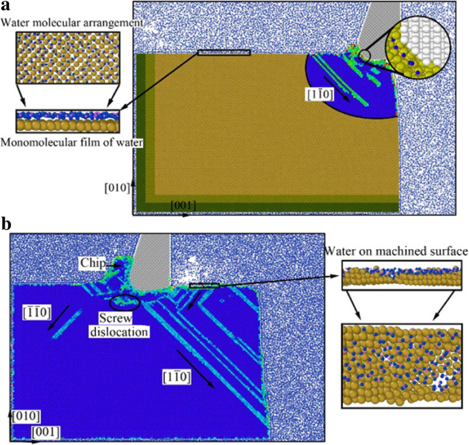
나노 절단 공정에서 수성 매체를 사용한 절단 시스템의 단면도(온라인 색상). 아 절단 거리 l =5nm. ㄴ 절단 거리 l =15nm
나노 절단 공정에서 슬립 변형은 절삭 공구의 초기 압축 전단 작용에 의해 발생하며 변형 에너지로 형성된 결정 격자에 저장됩니다. 변형 에너지 축적이 특정 수준에 도달하면 변형 에너지가 해제됩니다. 그런 다음 그림 2a와 같이 단결정 구리의 격자가 재배열되어 \( \left[1\overline{1}0\right] \) 방향으로 전위 핵 생성 및 확장이 발생합니다. Fig. 2a에서 물의 단분자막이 공작물 표면에 형성되어 있음을 알 수 있다. 또한, 물 분자는 그림 2a의 오른쪽 상단 그림과 같이 도구 칩 인터페이스의 작업 영역에서 공작물의 표면 아래로 침투합니다. 절삭 공구와 공작물 사이에 존재하는 물 분자의 윤활 작용으로 인해 절삭 공구의 압축 전단 작용이 감쇠됩니다. 그리고 변형 에너지 축적이 감소하고 전위가 불충분하게 확장됩니다. 또한 수성 매체는 절단 열을 많이 빼앗아 핵 전위 팽창 에너지가 충분하지 않습니다. 따라서 그림 2a와 같이 전위 확장이 불충분하고 공작물의 표면 아래 전위 라인이 눈에 띄지 않습니다.
절삭 공구가 전진하면서 가공물은 절삭 공구의 측면에서 발생하는 압출 및 마찰 작용을 받았습니다. 절삭 공구의 압출 및 마찰 작용으로 많은 수의 전위가 공작물의 표면 아래에서 핵 생성 및 확장됩니다. 이러한 전위의 일부는 경사면을 따라 위쪽으로 이동하고 궁극적으로 그림 2b와 같이 절단 칩으로 제거됩니다. 이러한 전위의 다른 부분은 절삭공구의 경사면을 따라 아래쪽으로 이동하고 절삭공구 측면의 압출 마찰 작용 후에 거칠기 가공된 표면으로 변형되며, 이는 그림 2b에서 "가공된 표면의 물 배열"로 표시됩니다. " 전위의 다른 부분은 \( \left[\overline{1}\overline{1}0\right] \) 및 \( \left[1\overline{1}0\right] \) 슬립 평면을 따라 안쪽으로 이동합니다. 그림 2b와 같이 나사 전위가 형성되어 공작물 내부에서 사라집니다. 칩 높이가 점차 증가하기 때문에 칩 앞의 물 분자는 나중에 절삭 공정에서 칩 위로 절삭 공구 뒤로 흐를 수 없습니다. 그리고 절삭 공구 뒤의 수중 매체의 밀도와 압력이 급격히 감소하여 나노 절삭 공정 중에 절삭 열이 제때 제거됩니다. 따라서 핵 생성 전위는 그림 2b와 같이 공작물 내부로 확장하기에 충분한 에너지를 갖습니다.
나노 절단 공정 중 단결정 구리의 전위 변형 및 국부적 원자 결정 구조를 설명하기 위해 CSP 및 DXA 분석 방법이 도입되었습니다. 분석 결과는 도 5에 도시된 바와 같이 나타내었다. 3, 4, 5, 6, 그 중 Fig. 도 3 및 도 4는 CSP 값 및 도 3 및 도 4에 따라 렌더링된다. 5번과 6번은 DXA 분석 결과로 채색됩니다.
<그림>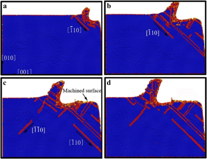
나노 절단 공정에서 수성 매체를 사용한 공작물의 표면 결함 분포. a의 절단 거리 , b , ㄷ , 및 d 각각 5nm, 8nm, 12nm, 15nm입니다.
<사진>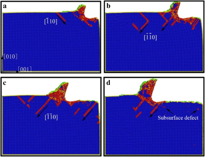
진공 환경에서 나노 절단 공정 중 공작물의 표면 아래 결함 분포. a의 절단 거리 , b , ㄷ , 및 d 각각 5nm, 8nm, 12nm, 15nm입니다.
<그림>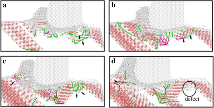
나노 절단 초기 단계의 공작물의 DXA 이미지. 전위는 다음 구성표에 따라 색상이 지정됩니다. 완전한 전위는 진한 파란색, Shockley 전위는 녹색, Stair-rod 전위는 분홍색, Hirth 전위는 노란색, Frank 전위는 하늘색, 미확인 전위는 빨간색입니다. a의 절단 거리 , b , ㄷ , 및 d 각각 7 nm, 8 nm, 9 nm 및 10 nm입니다.
<그림>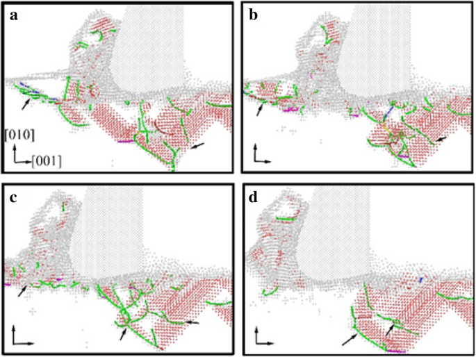
나노 절단 후기의 공작물 DXA 이미지. 전위의 채색 방식은 그림 5와 같습니다. a의 절단 거리 , b , ㄷ , 및 d 각각 17 nm, 18 nm, 19 nm 및 20 nm입니다.
수성 매체를 사용한 나노 절단 공정에서 공작물의 표면 아래 결함 분포가 그림 3에 나와 있으며, 여기서 물 매체는 전위 결함 전개를 보다 명확하게 관찰하기 위해 표시되지 않습니다. 노란색, 녹색, 빨간색 및 주황색 영역은 각각 표면 원자, 표면 결함 원자, 전위 원자 및 표면 아래 결함 원자를 나타냅니다. 수성 매체 없이 나노 절단 공정에서 가공물의 전위 분포와 확장은 그림 4와 같다. 두 그림에서 핵 전위가 \( \left[\overline{1}10 \right] \) 수성 매체를 사용한 나노 절단 과정에서 슬립 벡터, 그러나 진공 매체에서 나노 절단에서 \( \left[\overline{1}\overline{1}0\right] \) 슬립 벡터를 따라 확장 . 우리가 알고 있는 바와 같이, 절삭 공구의 전단 작용은 전위가 공구 전방 방향을 따라 확장되도록 하며, 이는 \( \left[\overline{1}10\right] \) 슬립 벡터입니다. 절삭 공구의 마찰 작용은 \( \left[\overline{1}\overline{1}0\right] \) 슬립 벡터인 직교 공구 이동 방향을 따라 이동하는 전위로 이어집니다. 진공 환경에서 나노 절단 공정 중 공작물에 대한 절삭 공구의 작용은 경사면의 전단 작용과 측면 마찰 작용이며 가공면 및 표면 아래 결함의 형성은 측면 마찰 작용에 의해 유발됩니다. 따라서 전위 확장은 진공에서 나노 절단 공정 동안 \( \left[\overline{1}\overline{1}0\right] \) 슬립 벡터를 따라 퍼집니다. 공구와 공작물 사이에 존재하는 물 분자의 윤활로 인해 절삭 공구의 마찰 작용이 감소합니다. 따라서 전단 작용은 가공된 표면 및 표면 아래 결함의 형성에 중요한 역할을 합니다. 따라서 전위는 주로 수성 매체를 사용한 나노 절단에서 \( \left[\overline{1}10\right] \) 슬립 벡터를 따라 확장됩니다.
무화과에서. 도 3 및 도 4를 참조하면, 나노 절단 공정에서 수중 매체의 표면 아래 결함의 규모가 진공에서보다 더 크다는 것을 알 수 있다. 실제로 전위 결함은 가공 영역 전체에 퍼져 공작물 내부 깊숙이 확장됩니다. 절단 열은 수성 매체에 의해 제거되고 결함 원자의 에너지가 감소합니다. 따라서 표면 아래 결함은 소멸될 에너지가 충분하지 않습니다. 따라서, 전위 결함 잔류물이 증가한다. 표면 아래 결함층의 깊이는 수성 매체를 사용한 나노 절단 공정에서 상대적으로 더 큽니다. 물 분자, 탄소 원자 및 구리 원자의 상호 작용으로 인해 절삭 공구와 공작물 사이의 압출 마찰이 약화되고 가공면의 형성 과정에서 가공면의 원자 무질서가 악화됩니다. 또한, 표면 아래의 결함 잔류물이 악화되고 표면 아래 잔류 응력이 증가합니다.
물 매체가 전위 결함 전개 과정에 미치는 영향을 더 잘 나타내기 위해 DXA 방법을 사용하여 수성 매체를 사용한 나노 절단 공정에서 공작물을 분석했으며 초기 단계와 후기 단계는 그림 5와 같습니다. 및 6, 각각. 그림 5d와 같이 두 개의 적층 결함 사이에 위치하는 나노 절단 공정의 초기 단계에서 가공된 표면 아래의 여러 층의 원자에 안정적인 결정 결함이 존재하는 것으로 나타났습니다. 결정 결함의 존재는 가공면의 품질에 영향을 미치고 가공면에 미세 균열이 발생하기도 합니다. 따라서 결함 진화 과정의 형성이 연구됩니다. Fig. 5a에서 볼 수 있듯이, 결함 형성 초기에 절삭공구 측면의 마찰 작용에 의해 많은 Shockley 부분 전위가 핵 생성됨을 알 수 있다. 이러한 Shockley 전위는 그림 5b와 같이 절삭 공구가 전진하는 동안 V자형 전위 루프로 진화합니다. 그 후, V자형 전위는 점진적으로 일련의 Shockley 부분 전위로 진화합니다. 마지막으로 부분 전위는 표면 아래의 잔류 결함으로 변환됩니다. 절단 열이 수성 매체에 의해 제거되기 때문에 결함이 있는 원자는 소멸되기에는 너무 적은 에너지를 가지며 가공된 표면 아래에 있는 움직이지 않는 결함으로 변형됩니다. 가공된 표면의 거칠기가 증가하고 표면 아래의 잔류 응력이 더 악화됩니다. 또한, 결함에 의해 표면 미세균열이 유발될 수 있다.
칩 제거 공정 중 절삭 공구의 전단 슬립 작용에 대한 수성 매체의 영향은 DXA 방법으로 조사되었으며, 이는 그림 6과 같습니다. 그림 6a에서 많은 Shockley 부분 전위가 핵 생성됨을 알 수 있습니다. 절단 도구의 전면입니다. 그리고 전단 슬립 평면은 이러한 전위에 의해 구성됩니다. 다음 절단 공정에서 연속 적층 결함 및 부분 전위가 핵 생성되고 전단 슬립 평면에서 확장됩니다. 절삭공구 앞의 전위의 핵형성과 움직임에 따라 절삭칩은 그림 6c와 같이 전단슬립면을 따라 점차적으로 제거된다. 한편, 공구 경사면의 압출 마찰 효과는 수성 매체의 윤활 작용으로 인해 감소됩니다. 그림 6a-d와 같이 전위 핵 생성 및 전파가 불충분하고 표면 아래 결함 잔류물이 나노 절단 공정 중에 명확하지 않습니다. 이에 따라 공작물에 대한 절삭 공구의 전단 작용이 더욱 중요해집니다. 따라서 형성된 칩은 나노 절단 공정에서 수성 매체의 참여하에 더 쉽게 제거됩니다. 그리고 동시에 주 절삭력이 감소합니다. 이에 대해서는 이 백서 뒷부분에서 자세히 설명합니다.
절단 공정에서 절삭 공구의 압출 및 전단 작용에 의해 재료 제거가 실현됩니다. 금속 재료의 강도, 강성 및 인성으로 인해 절삭 공구의 경사면은 재료 제거 과정에서 피삭재의 변형에 대한 저항으로 인해 생성된 반력이 발생합니다. 그리고 공구의 측면 표면은 가공된 표면의 마찰력 저항에 의해 영향을 받습니다. 이 힘이 함께 절삭력을 구성했습니다. 동시에 절삭칩의 전단변형과 절삭공구와 피삭재 사이의 마찰작용에 의해 가해진 가공물이 절삭열로 변환되어 가공물의 온도가 상승합니다. 재료 변형 에너지의 축적 및 방출과 함께 가공물의 표면 아래층에서 전위 핵 생성 및 팽창이 발생하여 절삭 거리에 따른 절삭력 및 절삭 열의 변동을 유발했습니다.
본 연구에서 수성 매체의 참여는 절삭력과 절삭열의 변화에 큰 영향을 미친다. 수성 매체를 사용하거나 사용하지 않은 나노 절단 공정에서 절단 거리에 따른 절단력의 변화 곡선은 그림 1 및 2와 같습니다. 도 7 및 도 8에서 흑색, 적색 및 청색 곡선은 각각 이송력(Fx), 후방력(Fy) 및 접선력(Fz)이다. 시뮬레이션에서 Z 방향에서 PBC가 채택되고 다이아몬드 공구가 Z 방향을 따라 기둥형이기 때문에 평균 접선력(Fz)은 두 그림 모두에서 0nN 수준에 있습니다. 7과 8.
<그림>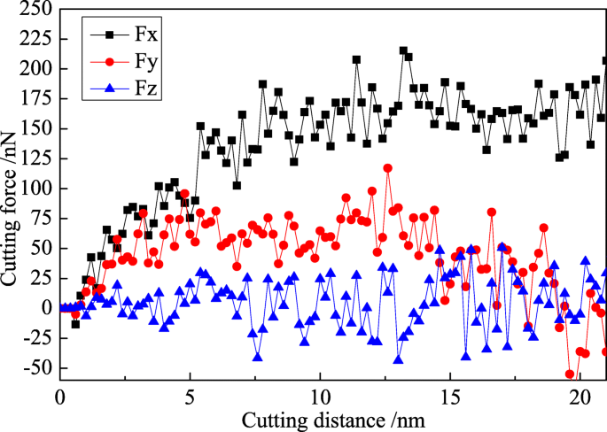
진공 환경에서 나노 절단에서 절단력의 변화 곡선
<그림>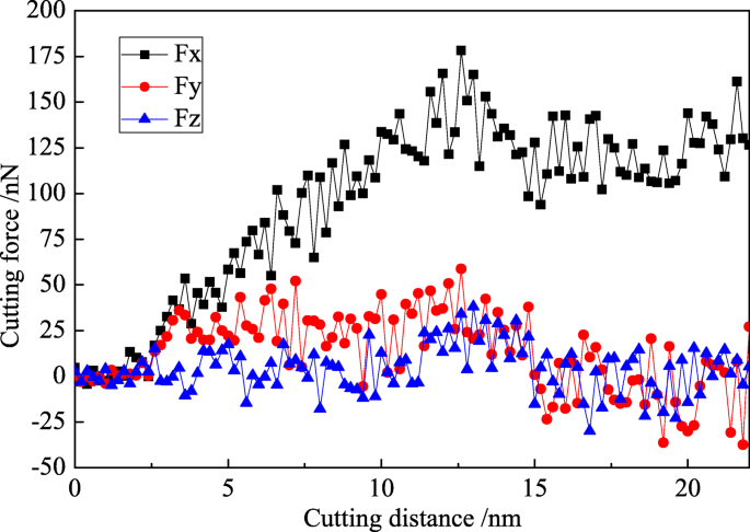
수성 매체를 사용한 나노 절단에서 절단력의 변화 곡선
절단공정은 그림 7과 같이 초기절삭단계와 안정절삭단계로 구분된다. 초기절삭단계에서는 이송력과 배력이 직선으로 급격히 증가한다. 그리고 절삭 공구가 공작물을 완전히 절단했을 때 최대값에 도달했습니다. 안정적인 절단 단계에서 절단력은 평형 위치에서 위아래로 변동하고 이송력은 200nN 이상에 도달하고 평균 절단력은 약 180nN입니다. 역력은 매우 작으며 후반 안정 절단 단계에서 점차 감소합니다. 소성력의 최대값은 100nN 미만이고 평균값은 약 50nN입니다. Generally speaking, the specific value between average back force and average feed force (Fy/Fx) represents the friction coefficient between tool material and workpiece material in machining process. In this research, the friction coefficient between diamond and monocrystal copper is 0.278 under vacuum environment.
The feed force and the back force are decreased in nano-cutting with water media compared with vacuum environment, as shown in Fig. 8. The maximum feed force reaches 150 nN, and the mean feed force fluctuates at 120 nN. The variation tendency of back force is similar with the back force in vacuum environment, and the mean force is at about 25 nN. In nano-cutting process with the use of water medium, the friction coefficient between the cutting tool and the workpiece is reduced due to the lubrication of water. And then the frictional resistance suffered by the flank surface of cutting tool is reduced, which effectively enhances the extrusion shearing action of the rake surface of cutting tool. The removal of the workpiece material is easier to be removed. Hence, the cutting force is reduced. It can be seen from the foregoing analysis that the water molecules acted as a lubricant to prevent the friction between the cutting tool and the workpiece. Therefore, the values of feed force and back force are reduced in the water media. The specific value between the feed force and the back force is 0.208. In another words, the frictional coefficient between diamond and copper in water media is 0.208, much fewer than they are in vacuum environment (0.278).
Compared with the fluctuation of the Fy in Figs. 7 and 8, it is indicated that the Fy component decreases considerably after 15 nm of cutting distance in both cases with vacuum and water media while the Fx value is almost stable until 20 nm of cutting distance. The dynamic balance between dislocation nucleation and annihilation is achieved, and the chip is removed steadily in nano-cutting process, which results in the cutting force almost stable with the cutting distance before 20 nm. When the cutting process is carried out at a certain distance (15 nm in this research), the dynamic equilibrium between the new dislocation nucleation and the previous dislocation annihilation is established. And the scale of the internal defects of the workpiece is stabilized at a certain level. The dislocation nucleation and annihilation applied an effect on cutting tool along +Y direction, which leads to the Fy component decrease. Besides, the stable cutting chip is removed after 15 nm of cutting distance, and the applied force on the cutting tool from the chip is decreased along the Y direction. Thereby, the value of Fy is reduced. However, when the cutting distance is greater than 15 nm till 20 nm, the emotion of dislocation defect and the removal of chip cannot bring a different influence on the cutting tool along the X direction. Therefore, the value of main cutting force (Fx) is almost stable.
The temperature distribution of the workpiece during the nano-cutting process with and without the use of aqueous media is shown as Fig. 9. The cutting distances of Figs. 9a and b and Figs. 9c and d are 5 nm and 12 nm, respectively. It can be seen from Figs. 9b and d that the temperature of workpiece is distributed as a concentric gradient. The highest temperature is spread all over shear-slip zone and friction zone of the workpiece in a vacuum environment, which is above 420 K. The temperature of the chip and machined surface is higher than other regions, which is ranged from 360 to 390 K. For the whole workpiece, the temperature is at a high level, which is ranged from 340 to 360 K. From Figs. 9a and c, the temperature of the workpiece is also distributed as a concentric gradient and the highest temperature is distributed at the top area of the chip, which is around 370 K. The temperature value of the whole workpiece is at a lower level which is lower than 320 K. The temperature of the shear-slip area, the friction zone, and the machined surface are higher than other areas, which is ranged from 320 to 340 K.

Temperature distribution of workpiece in nano-cutting. 아 및 c are in water media, b 그리고 d are in vacuum environment
The highest temperature area of workpiece is transferred from the friction area to the cutting chip during nano-cutting process with water media as shown in Fig 9. And the highest and whole temperature of the workpiece are significantly reduced with the additional use of water media, and the temperature drop reached about 40–60 K. Due to the lubrication effect of water molecules, the friction between cutting tool and machined surface is reduced during nano-cutting process with water media. Hence, the temperature of the friction area declined dramatically. Meanwhile, the maximum shearing deformation occurred at the chip area and the maximum lattice deformation energy is stored in the chip, which makes the temperature of the chip higher than the friction area. Therefore, the highest temperature area is transferred from friction area to the cutting chip. Synchronously, a large amount of cutting heat is taken away by the water media which play a role in cooling the tool, workpiece, and cutting area. And the thermal movement of the monocrystal copper molecules is weakened. Furthermore, the kinetic energy of atomic thermal motion and the lattice deformation energy are decreased significantly. Therefore, the overall temperature and the highest temperature of the workpiece is reduced, whose degree of reduction arrived at 40–60 K. Finally, the thermal stress and thermal deformation of the workpiece are significantly reduced. Because of the participation of water media, the friction action between the flank surface of cutting tool and workpiece is weakened in cutting process. Then, the generation of heat by friction between cutting tool and workpiece is reduced. Thereby, the highest temperature area of the workpiece is transferred from the friction area of flank surface to the chip area. More importantly, the cooling effect and lubrication of water media will affect the nucleation, expansion, and annihilation of the dislocation in subsurface of the workpiece and ultimately affect the formation and evolution of the subsurface damage layers of the workpiece.
In order to clearly identify the subsurface defects of the workpiece in nano-cutting, the CNA method is used to analyze the workpiece after nano-cutting. The workpiece is colored by different atomic structure. The defect structural distribution of the workpiece during nano-cutting process with and without the use of aqueous media is shown as Figs. 10 and 11, in which the green, red, blue, and grey are FCC, HCP, BCC, and unknown structure, respectively.

Subsurface defect evolution of workpiece in nano-cutting without aqueous media. The green, red, blue, and grey area are representative of FCC, HCP, BCC, and unknown structure. The cutting distances of a, b, c, and d are 1 nm, 3 nm, 8 nm, and 15 nm, respectively

Surface and subsurface defect distribution in nano-cutting for workpiece with water media. The green, red, blue, and grey area are representative of FCC, HCP, BCC, and unknown structure. The cutting distances of a, b, c, d, e, and f are 3 nm, 8 nm, 12 nm, 15 nm, 18nm, and 20nm respectively
In nano-cutting process under vacuum environment, dislocation nucleation occurred at the subsurface of workpiece under the extrusion and shearing action of the cutting tool, and the crystal structure is transformed into BCC, which is shown as Fig. 10a. The nucleated dislocation is extended along \( \left[\overline{1}\overline{1}0\right] \) direction, and the crystal structure is transformed into HCP. The crystal structure of many atoms in the shear-slip region become BCC, as shown in Fig. 10b. Two partial dislocations are extended along the \( \left[\overline{1}\overline{1}0\right] \) and \( \left[1\overline{1}0\right] \) directions, hindered each other, and be composed of Lomer-Cottrell dislocation lock. Finally, a typical V-shaped dislocation loop is formed, as shown in Fig. 10c. Part of the atoms in the shear-slip zone are moved upward along the rake face and are removed as cutting chip. The other part of the atoms are migrated downward along the flank face and are formed into the roughness machined surface by the extrusion and friction of the cutting tool, as shown in Fig. 10d.
The subsurface defect distribution and evolution of workpiece in nano-cutting with the use of water media is shown as Fig. 11. It can be seen from the figure that the mechanisms of dislocation nucleation and crystal structure transformation are similar with the cutting process in vacuum environment. The main difference is that the dislocation nucleation and expansion is insufficient in the nano-cutting process of water media. Besides, there are many stacking faults nucleated in the subsurface of the workpiece. The structure of stacking faults is transformed into HCP structure. Nevertheless, a typical defect “similar-to-grain boundary (SGB)” is formed in the subsurface of the workpiece.
In nano-cutting process, under the action of extrusion, shearing and friction by cutting tool, intense deformation of the workpiece is generated. Plenty of deformation energy and cutting heat are produced. The atomic lattice reconfiguration of subsurface is produced by the release of cutting heat and strain energy. And the subsurface defects and local crystal structure transformation are formed, as shown in Fig. 11a and 11b. When the water media participated in the nano-cutting process, most of the heat and energy is taken away. Hence, the dislocation defects have inadequate energy to extension and movement. Furthermore, the stacking faults are annihilated in the subsurface of the workpiece where the crystal defect structure stayed behind, as shown in Fig. 11c, whereafter these crystal defect structures are connected as a whole and are composed of the subsurface damage (SSD) layer together with the newly formed dislocations, as shown in Fig. 11d. After the following MD relaxation, some subsurface dislocation defects are disappeared and transformed into FCC structure, and the structure similar to “grain” is formed between machined surface and subsurface defects layer, as shown in Fig. 11e, while the original subsurface defects are transformed into a typical structure “similar-to-grain boundary (SGB),” as shown in Fig. 11f. On the SGB structure, a typical V shape dislocation loop is formed, as shown in Fig. 11e, f.
The metamorphic layer is obviously formed by the influence of the formation of SGB and “grain” structure in the subsurface of workpiece. Moreover, the new formed crystal structures which are similar with polycrystalline material can influence the mechanical performance and processability of single-crystal materials. Besides, it will affect even the performance of machined nano-components.
Based on the established MD models of single-crystal copper with and without the use of aqueous media, the simulation of nano-cutting process is carried out. The effects of fluid media on material removal and subsurface defect evolution are analyzed. The subsurface defect evolution, variation of the cutting force, the temperature distribution, and the subsurface defects crystal structure transformation of the workpiece are investigated by using CSP, DXA, and CNA methods. The novel results can be summarized as follows.
(1) The material removal of workpiece is realized by the shearing extrusion action of cutting tool on workpiece; the participation of water media has no effect on the mechanism of materials removal. Due to the lubrication action of water molecules existing between the cutting tool and the workpiece, the deformation of workpiece is decreased, the cutting force is reduced, and the height of cutting chip and depth of subsurface damage layer are lowered.
(2) The highest temperature area is transferred from the friction area to the cutting chip during nano-cutting process with the additional use of water media. And the highest and whole temperature of the workpiece are significantly reduced, and the temperature drop reached about 40–60 K. Thereby, the thermal deformation of the workpiece is reduced and the amount of subsurface defect atoms is decreased.
(3) In the subsurface layer of the workpiece, the crystal structures of nucleated dislocations are transformed into BCC, and the extended dislocations are transformed into HCP. The atomic crystal structures in the shear-slip region are becoming BCC. Under the effect of fluid media, the subsurface defects are transformed into a typical defect structure “similar-to-grain boundary (SGB)” in SSD layer, which can influence the mechanical performance and processability of single-crystal materials. Besides, it will affect even the performance of the machined nano-components.
Molecular dynamics
Centro-symmetry parameter
Common neighbor analysis
Dislocation extract algorithm
Periodic boundary condition
Embedded-atom method
Lennard-Jones
Face center cubic
Close-packed hexagonal
Body centered cubic
Icosohedral
Similar-to-grain boundary
Subsurface damage
나노물질
산소 연료 절단이란 무엇입니까? 순산소 용접 및 순산소 절단은 연료 가스(또는 가솔린이나 휘발유와 같은 액체 연료)와 산소를 사용하여 금속을 용접하거나 절단하는 공정입니다. 프랑스 엔지니어 Edmond Fouche와 Charles Picard는 1903년에 최초로 산소-아세틸렌 용접을 개발했습니다. 공기 대신 순수 산소를 사용하여 화염 온도를 높여 실내 환경에서 공작물 재료(예:강철)를 국부적으로 녹일 수 있습니다. 일반적인 프로판/공기 화염은 약 2,250K(1,980°C, 3,590°F), 프로판/산소 화염은 약 2,52
가공은 광범위한 기술과 기술을 포괄하는 제조 용어입니다. 동력 구동 공작 기계를 사용하여 공작물에서 재료를 제거하여 의도한 디자인으로 성형하는 과정으로 대략 정의할 수 있습니다. 대부분의 금속 부품과 부품은 제조 과정에서 어떤 형태의 가공이 필요합니다. 플라스틱, 고무 및 종이 제품과 같은 기타 재료도 일반적으로 기계 가공 공정을 통해 제조됩니다. 머시닝이란 무엇이며, 그 프로세스는 무엇이며, 이를 위해 사용되는 도구와 기술에 대해 자세히 알아보겠습니다. 가공이란 무엇입니까? 가공은 더 큰 재료 조각에서 원하지 않는 재료를 제