

나노물질

산업 제조
탄소나노튜브(CNT)는 높은 기계적 강도, 큰 종횡비, 높은 표면적, 독특한 광학적 특성, 높은 열 및 전기 전도성을 포함한 특성의 독특한 조합으로 인해 상당한 관심을 끌었습니다. 전자(트랜지스터, 에너지 생산 및 저장)에서 생명공학(이미징, 센서, 액추에이터 및 약물 전달) 및 기타 애플리케이션(디스플레이, 포토닉스, 복합재 및 다기능 코팅/필름)에 이르는 영역. CNT의 제어된 성장, 조립 및 통합은 현재 및 미래의 나노튜브 응용 프로그램의 실질적인 실현에 필수적입니다. 이 리뷰는 다양한 애플리케이션을 위한 CNT 조립 및 통합 분야의 현재까지 진행 상황에 중점을 둡니다. 팁 성장 및 베이스 성장 모델의 세부 사항을 포함하는 아크 방전, 레이저 제거 및 화학 기상 증착(CVD)을 기반으로 하는 CNT 합성이 먼저 소개됩니다. 촉매 컨디셔닝, 클로닝, 시드 및 템플릿 기반 성장과 같은 방법을 사용한 CNT 구조 제어(키랄성, 직경 및 접합)의 발전에 대해 자세히 살펴본 다음 선택적 표면 화학, 겔 크로마토그래피를 사용한 성장 후 CNT 정제 기술을 살펴봅니다. 및 밀도 구배 원심분리. 촉매 패터닝, 산림 성장 및 복합 재료를 기반으로 한 다중 CNT에 대한 다양한 조립 및 통합 기술은 포토리소그래피, 전사 인쇄 및 잉크젯 인쇄, 유전영동(DEP) 및 스핀과 같은 다양한 솔루션 기반 기술을 사용하여 서로 다른 기판에 정렬/배치하는 것과 함께 고려됩니다. 코팅. 마지막으로 에너지 저장, 트랜지스터, 조직 공학, 약물 전달, 전자 암호 키 및 센서와 같은 분야에서 CNT의 현재 및 새로운 응용 분야의 몇 가지 문제를 고려합니다.
탄소 나노튜브(CNT)는 1nm 미만에서 10nm 범위의 직경을 갖는 흑연 시트(일명 그래핀)로 만들어진 길고 속이 빈 원통형 세관 구조입니다[1]. CNT는 이러한 그래핀 층이 실린더로 롤링되는 방식에 따라 다른 전자 특성을 나타냅니다. 나노튜브는 단일벽 탄소나노튜브(SWCNT)라고 하는 단일벽 구조이거나 다중벽 탄소나노튜브(MWCNT)라고 하는 많은 벽을 가질 수 있습니다. SWCNT는 전기적으로 반도체 및 금속성 SWCNT(s-SWCNT 및 m-SWCNT)로 더 분류할 수 있지만 MWCNT는 주로 금속성 거동을 나타냅니다. 저비용, 가벼움, 높은 종횡비 및 표면적, 독특한 광학적 특성, 높은 열 및 전기 전도성 및 높은 기계적 강도와 같은 CNT의 새롭고 유용한 특성은 CNT를 광범위한 전자 제품에 적합하고 흥미롭게 만듭니다. , 생물 의학 및 기타 산업 응용 프로그램. 예를 들어, CNT는 능동 소자 및 미래 집적 회로의 인터커넥트로서 'CMOS를 넘어서' 전자 제품에 유망합니다[2].
CNT는 중공 구, 타원체 또는 원통형 튜브와 같은 케이지 같은 구조의 형태로 연결된 원자를 가진 탄소 동소체 그룹인 풀러렌 계열의 일부입니다[3]. 풀러렌은 연결된 6각형 및 5각형 고리의 그래핀 시트로 구성되어 곡선 구조를 제공합니다. 그래핀은 2차원 육각형 격자에 배열된 단일 탄소 원자층으로 구성된 탄소 동소체입니다. 원자가 밴드와 전도 밴드 사이에 중첩이 있는 반금속입니다. 즉, 밴드갭이 0입니다[1]. 벅민스터풀러렌(buckyball/C60 가장 일반적인 구형 풀러렌 중 하나인 )은 60개의 탄소 원자를 갖는 나노크기 분자이며, 각 원자는 3개의 인접한 다른 원자에 결합되어 육각형과 오각형을 형성하고 끝이 구로 구부러져 있습니다. C70 분자는 화학적으로 안정적인 것으로 알려진 또 다른 구형 풀러렌입니다. 또한 C28과 같은 다른 작은 준안정 종 , C36 및 C50 , 발견되었습니다. 풀러렌은 오랫동안 자연에 존재했다고 믿어집니다. C60 형태의 풀러렌 미량 , C70 , C76 , C82 및 C84 , 그을음에 숨겨진 것으로 밝혀졌습니다[3, 4]. 나노튜브는 sp 2 로 구성됩니다. - sp 3 보다 더 강한 하이브리드 탄소 결합 -다이아몬드에서 발견되는 하이브리드 탄소 결합으로 나노튜브의 뛰어난 강도와 강성을 제공합니다. 또한, 매우 높은 전기 전도성[5, 6], 높은 전하 캐리어 이동도[7], 높은 화학적 안정성[8, 9], 큰 비표면비[10], 높은 종횡비[11], 우수한 기계적 특성[12, 13] 및 우수한 열전도율[14], 일부 SWCNT는 초전도성을 나타냄[15, 16]. 이러한 특성은 CNT를 나노과학 및 전자 연구에서 중요한 주제로 만듭니다[17].
개별 SWCNT의 비표면적(SSA)은 이론적으로 1315m 2 로 얻어졌습니다. g −1 ; 그러나 측정된 표면적은 튜브의 번들링, 덩어리 및 순도 때문에 훨씬 더 낮습니다[10]. 예를 들어, SSA 값이 150~790m 2 인 SWCNT 표본 g −1 얻었다[10]. MWCNT의 경우 벽의 수가 SSA를 결정하는 주요 매개변수입니다. 측정된 일부 SSA 값에는 680–850m 2 가 포함됩니다. g −1 이중벽 CNT 및 500m 2 용 g −1 3벽 CNT의 경우 [10]. 또한 CNT는 주목할만한 기계적 특성을 가지고 있습니다. 개별 MWCNT의 탄성 계수는 약 1TPa인 반면 MWCNT의 인장 강도 범위는 11~63GPa입니다[12, 13]. 반면, 단일 SWCNT의 경우 약 22GPa의 인장 강도 값이 얻어졌습니다[12]. 개별 SWCNT의 Young's modulus는 직접 측정되어 0.79~3.6 TPa[12, 13, 18]인 반면 개별 MWCNT의 경우 0.27~2.4 TPa의 값이 얻어졌습니다[12, 19]. 얇은 MWCNT의 압축 강도는 100에서 150GPa 사이인 것으로 추정되었습니다[20]. CNT는 또한 우수한 열적 특성을 가지고 있습니다. 개별 SWCNT는 3500~6600Wm −1 사이의 열전도율 값을 가질 수 있습니다. K −1 다이아몬드의 열전도율을 초과하는 실온에서 [14, 21], 개별 MWCNT의 열전도율은 600 ~ 6000 Wm -1 입니다. K −1 [21]. CNT는 또한 흥미로운 차원 특성을 가지고 있습니다. 가로 세로 비율(길이 대 지름) 값은 매우 높을 수 있습니다. 일반적인 CNT 직경 값은 0.4에서 40 nm(즉, 약 100배)까지 다양하지만 길이는 10,000배까지 다양하여 55.5cm에 도달할 수 있으므로 종횡비가 매우 높을 수 있습니다[11].
CNT는 또한 독특한 전자 특성을 가지고 있습니다. CNT의 고유한 전자 특성은 고유한 저차원 밴드 구조 및 양자 구속 캐리어와 본질적으로 관련이 있습니다. SWCNT는 튜브의 키랄성(chirality)이라고 하는 튜브 축에 대한 그래핀 격자의 직경과 방향에 따라 금속성 또는 반도체성일 수 있습니다[1, 22]. 기저 벡터 a 1 그리고 a 2 그래핀 격자를 결정한다. 키랄 벡터(C ), 이는 결국 CNT 둘레가 될 그래핀 시트의 측면에 해당하며 다음과 같이 주어집니다. C =나 1 + 엄마 2 , 여기서 n 그리고 나 정수입니다. 그래핀 시트는 그림 1a-c와 같이 세 가지 다른 클래스의 SWCNT를 생성하기 위해 다른 방식으로 말릴 수 있습니다. 또한 각 CNT의 전자적 특성은 키랄 벡터에 의해 결정되는 튜브의 기하학적 구조에서 발생합니다. m =0인 경우 , C a 1 또는 a 2 나노튜브는 지그재그 CNT라고 하며, n =m , C 정확히 a 사이의 방향을 따라 놓여 있습니다. 1 그리고 a 2 튜브는 안락의자 나노튜브라고 합니다. 마지막으로 n ≠ 일 때 키랄 나노튜브가 형성됩니다. . 그림 1b는 키랄 지수와 해당 키랄 각도를 기반으로 하는 다양한 유형의 CNT가 어떻게 정의되는지 보여줍니다. 소위 구역 접기 방식[23] 내에서 분석에 따르면 안락의자 튜브는 항상 금속성인 반면 지그재그 튜브의 3분의 2는 반도체입니다. 더 일반적으로, 모든 SWNT의 2/3는 나머지 금속과 함께 반도체 또는 작은 밴드 갭(준금속)을 소유하는 것으로 예측됩니다.
<그림>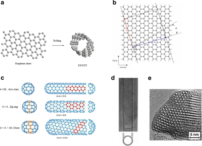
아 단일 층의 흑연을 압연하여 SWCNT를 형성합니다. ㄴ 이상적인 흑연 시트에서 CNT를 형성하는 그림. 키랄 벡터 C의 두 끝 어 1D 격자 벡터 T가 있는 나노튜브를 만들기 위해 중첩됩니다. 및 키랄 각 ϴ . 아 1 그리고 a 2 는 2D 흑연의 기본 격자 벡터입니다(흰색 점은 격자 파인트를 나타냄). 지그재그 및 안락의자 포장 방향도 표시됩니다. ㄷ 키랄성을 기반으로 한 다양한 유형의 CNT. [22]에서 수정. d 직경 5.5 nm의 이중벽 CNT의 전자현미경 사진. [78]에서 수정. 이 삼각형 격자에 포장된 ~ 100 SWCNT 번들의 전자 현미경 이미지. [17]에서 수정
CNT는 전하 캐리어 이동도가 매우 높기 때문에 다양한 전자 장치 응용 분야에서 고려할 가능성이 있습니다[24]. SWCNT가 캐리어 이동도가 높은 고급 준 1차원(1D) 재료임을 보여주는 많은 진전이 있었습니다. CNT의 캐리어 이동도 추정값 범위는 20cm 2 입니다. V −1 s −1 [7] 매우 큰 값(~ 10 4 또는 그 이상) 반도체 튜브 및 탄도 금속 튜브 [25]. 10 7 사이의 전류 밀도 센티미터 −2 및 10 8 센티미터 −2 SWCNT에 대해 달성할 수 있으며 SWCNT는 약 20μA의 전류를 전달할 수 있습니다[26]. 탄도 SWCNT는 6.5~15kΩ 사이의 저항을 나타냅니다. MWCNT는 일반적으로 금속이며[1] 10 6 범위의 매우 높은 전류 전달 용량을 가집니다. ~ 10 9 센티미터 −2 [26, 27]. 반도체 CNT의 밴드갭은 직경에 반비례하는 것으로 나타났으며(그림 2a) E로 표시됩니다. 갭 =2γ 0 아 C-C /d , 여기서 y 오 C-C 밀착 결합 중첩 에너지(2.45 eV)를 나타냅니다. a C-C 가장 가까운 이웃 C-C 거리(0.142 nm) 및 d 는 튜브의 직경입니다[28, 29]. 예를 들어 반지름이 0.2nm인 반도체 CNT는 밴드 갭이 약 2.2eV인 반면 반지름이 1.4nm인 튜브는 밴드 갭이 약 0.4eV입니다[30].
<그림>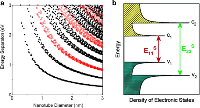
아 탄소 나노튜브의 밴드 갭 에너지와 직경에 관한 Kataura 플롯. 여기서 빨간색 원은 반도체성 CNT를 나타내고 검은색 원은 금속성 CNT를 나타냅니다. [32]에서 수정. ㄴ 반도체 CNT의 상태 밀도와 VHS 피크(예리한 최대값으로 표시)를 보여주는 개략도. 화살표는 광 흡수 및 방출 메커니즘을 나타냅니다. [36]에서 수정
파동 함수 경계 조건이 (n , 나 ) 튜브의 지수 또는 키랄성. 따라서 흡수, 광발광 및 라만 분광법과 같은 광학적 특성은 광자로 CNT 샘플을 조사함으로써 CNT에 대한 빠르고 비파괴적인 연구를 광범위하게 수행하는 데 사용할 수 있습니다[31,32,33]. CNT는 또한 빛에 노출될 때 독특한 광점화 특성을 나타내[34, 35], 결과적으로 음향파가 생성되고 CNT가 산화됩니다. 광학 분광법의 결과는 Kataura 플롯으로 기록할 수 있으며, 여기서 각 점은 광학 전이 에너지 E를 나타냅니다. ii (나 =1, 2, 3, ...) 특정(n, m) ) SWCNT는 그림 2a와 같이 튜브 직경의 함수로 표시됩니다. 1D 결정체는 에너지의 연속적인 함수로서의 상태 밀도(DOS)를 갖지 않지만, 불연속적인 스파이크에서 상승 및 하강하는 스파이크와 같은 DOS를 가지고 있습니다. 이러한 날카로운 스파이크 또는 Van Hove 특이점(VHS)은 CNT의 독특한 광학 특성을 만듭니다[32]. CNT의 광 흡수는 날카로운 피크의 존재로 인해 대부분의 벌크 재료에서의 흡수와 다릅니다. SWCNT가 빛을 흡수할 때 가전자대의 VHS에 있는 전자는 전도대의 해당 에너지 준위로 상승합니다. 나노튜브에서 광 흡수는 v 2 c에게 2 (에너지 E 22 ) 또는 v 1 c에게 1 (이 11 ) 수준(그림 2b) [36]. 이러한 전이를 조사한 다음 나노튜브 유형을 식별하는 데 사용합니다[32].
CNT의 광 흡수 특성 외에도 일반적으로 연구되는 또 다른 광 특성은 광발광입니다. 광발광은 CNT 샘플에서 반도체 나노튜브 종의 양을 측정하는 데 사용됩니다. 반도체 SWCNT는 광자에 의해 여기될 때 근적외선을 방출하며, 이를 광발광이라고 합니다[37]. 반도체 SWCNT의 전자가 여기광을 흡수하여 E 22 전이(반도성 SWCNT에서 원자가에서 전도대로의 전자 전이), 전자-정공 쌍이 생성됩니다. 전자와 정공은 모두 c에서 빠르게 이완됩니다. 2 c에게 1 그리고 v에서 2 v로 1 상태를 각각 나타냅니다. 마지막으로 c 1 - v 1 빛을 방출하는 전이 [32]. 금속 튜브에서는 여기자 발광이 생성될 수 없습니다. 전자-정공 쌍을 생성할 수는 있지만 홀은 금속에서 사용할 수 있는 많은 전자 중 다른 전자에 의해 즉시 채워지므로 여기자가 생성되지 않습니다.
CNT 특성화를 위한 또 다른 광학 기술인 라만 분광법은 반도체 및 금속 튜브를 감지할 수 있는 능력이 있으며 [38] 라만 현미경을 통해 좋은 공간 분해능도 제공할 수 있습니다. 라만 분광법에서 광자는 CNT 샘플을 여기시키는 데 사용되며 샘플의 포논에 의해 산란됩니다. 여기 광자와 방출된 광자 사이의 주파수 변화 분석은 주로 직경 의존 방사형 호흡 모드를 통해 샘플에 어떤 종류의 CNT가 있는지 알려줍니다[23]. SWCNT의 라만 산란은 또한 공명할 수 있습니다. 즉, 여기 레이저 에너지와 동일한 밴드갭 중 하나를 갖는 튜브만이 향상된 흡수 단면으로 선택적으로 조사됩니다.
위에서 설명한 CNT 속성에 대해 선택된 숫자 데이터는 표 1에 나열되어 있습니다.
고유하고 바람직한 특성으로 인해 CNT는 현재까지 많은 응용 분야와 여러 상용 제품에 통합되었습니다.
반도체 CNT는 전계 효과 트랜지스터(FET)에 사용되었습니다[7, 45,46,47,48](그림 3은 개략도를 보여주고 I -V 상이한 게이트 전압에 대한 스위칭을 나타내는 CNT 전계 효과 트랜지스터(CNTFET)의 특성); 금속성 CNT는 인터커넥트로 사용된다[49, 50]. 단일벽 나노튜브와 다중벽 나노튜브는 다양한 THz 응용 분야(아래 설명)와 쇼트키 다이오드에도 사용되었습니다[51]. CNT는 현재 효율적인 에너지 저장을 위해 리튬 이온 배터리에 사용되고 있습니다[52, 53]. 수소 연료 전지[54] 및 CNT 코팅은 암모니아, 수소 및 메탄과 같은 가스를 감지하는 데 광범위하게 사용되었습니다[55]. 초정렬 탄소 나노튜브 필름은 액정 디스플레이(LCD)에 사용되었습니다[56]. CNT는 또한 투명 전도성 필름에서 응용을 발견했습니다[57].
<그림>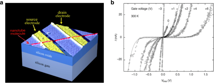
아 초기 CNTFET 데모의 개략도. 트랜지스터는 소스 전극과 드레인 전극을 연결하는 나노튜브 채널로 캐리어를 유도하는 실리콘 기판(백 게이트)에 게이트 전압을 적용하여 켜질 수 있습니다. [45]에서 수정. ㄴ 나 -V 다른 게이트 전압에서 옴과 비선형 거동 사이의 스위칭을 보여주는 CNTFET의 특성. [48]에서 수정
CNT 재료 복합 재료는 향상된 특성을 갖는 것으로 밝혀졌습니다. 예를 들어, CNT 강화 에폭시 합성물은 순수 에폭시 매트릭스에 비해 인장 강도가 24.8% 증가하는 것으로 나타났습니다[58]. 또한 탄소 섬유 강화 고분자 복합 재료에 소량의 자기적으로 정렬된 CNT를 도입함으로써 굴곡 탄성률과 하중 지지 능력이 각각 46%와 33% 증가했습니다[59]. 또한 CNT와 팽창성 난연제로 채워진 열가소성 폴리우레탄(TPU) 기반 복합 재료는 우수한 난연성, 신속한 자가 소화, 우수한 전자파 간섭 차폐 특성 및 증가된 전기 전도성을 달성하는 것으로 나타났습니다[60]. 또한 CNT 분말을 폴리머와 혼합하면 하중 지지 응용 분야에서 강성, 강도 및 인성이 증가합니다[61, 62]. MWCNTs - 탄소 나노튜브 합성물인 자기형광 탄소 양자점은 암 치료에서 표적 약물 수송을 위한 운반체로 사용되었습니다[63]. 분산된 CNT를 포함하는 나노유체는 향상된 열전달 특성을 나타냅니다[64]. 질소 도핑된 CNT(N-CNT)는 과일 주스에서 비스페놀을 추적하기 위해 식품 분석에서 흡착제로 사용할 수 있습니다[65].
연구원들은 SWCNT를 새로운 고주파 장치의 빌딩 블록으로 사용하기 시작했습니다[66]. 외부 자기장과 전기장이 있는 상태에서 특정 나노튜브는 강력한 테라헤르츠(THz) 광학 전이를 일으켜 THz 장치에서 조정 가능한 광학 활성 물질로 유용합니다. THz 애플리케이션에서 CNT를 사용하기 위한 몇 가지 제안이 개발되었습니다. 여기에는 나노튜브로부터의 효율적인 고장 전자 방출을 활용하는 나노클라이스트론, 대구경 반도체 나노튜브의 음의 차동 전도도에 기반한 장치, THz 영역에서 작동하는 단일 및 다중벽 탄소 나노튜브 안테나가 포함됩니다[66,67,68] . 고유한 전자 특성으로 인해 CNT는 테라헤르츠(THz) 방사선의 소스로 사용됩니다. 소형의 신뢰할 수 있는 THz 방사선 소스를 만드는 것은 현재 사용 가능한 소형 및 저가 THz 소스가 없기 때문에 현대 응용 물리학에 매우 중요합니다[66,67,68]. THz 복사는 전자기 스펙트럼에서 마이크로파와 적외선 사이에 있습니다. 이 주파수 범위에서 전자 수송과 광학 현상이 합쳐지고 고전파는 양자역학적 광자가 된다. THz 범위의 이러한 독특한 위치는 탄소 기반 나노 물질을 사용하는 것과 같이 물질의 전자적 특성과 광학적 특성 사이의 간극을 연결하는 새로운 접근 방식을 통해서만 연구할 수 있음을 의미합니다. 연구원들은 또한 광전지[69] 및 적외선(IR) 감지[70]를 포함한 분야에서 CNT의 사용을 조사하고 있습니다.
나노 규모에서 합성을 위한 반응기로 CNT를 사용할 가능성은 또 다른 연구 영역입니다[71]. 전기촉매 산소 환원 반응(ORR) 및 산소 발생 반응(OER)을 위한 촉매 지지체로 CNT를 사용하는 것이 널리 보급되고 있습니다[72,73,74,75,76]. 특히, 다양한 연구에서 효율적인 ORR 및 OER 반응을 위해 질소 도핑된 탄소 나노물질을 사용하는 것으로 나타났습니다. 여기서 이러한 CNT 전극은 백금과 같은 금속에 비해 향상된 안정성과 전기촉매 활성을 보여줍니다[76, 77].
일반적으로 많은 수의 CNT의 배치, 유형, 방향 및/또는 구조에 대한 정확한 제어는 위에서 언급한 것과 같은 주어진 애플리케이션에 대한 성능을 최적화하기 위해 필요합니다. 이 리뷰에서는 다양한 접근 방식을 기반으로 한 탄소 나노튜브 조립 및 통합의 진행 상황을 검토하고 논의합니다. 특히, 우리는 먼저 성장 중 직접 및 성장 후 접근 방식을 통해 개별 CNT를 제어하는 기술에 중점을 둡니다. 그런 다음 결과 구조 및 앙상블과 함께 많은 수의 나노튜브를 병렬로 통합하기 위해 개발된 방법을 조사합니다. 마지막으로, CNT 제조 및 조립 분야에서 지난 20년 동안의 엄청난 발전에도 불구하고 우리는 CNT를 사용하는 현재 및 신흥 응용 프로그램 모두에 남아 있는 중요한 과제를 강조합니다. 이 논문의 개략도는 그림 4에 나와 있습니다.
<그림>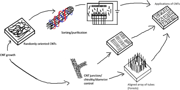
논문의 개략도. 이 리뷰에서는 개별 튜브(예:키랄성, 접합부 및 직경)에서 다양한 정제, 조립, 정렬 기술 및 광범위한 응용을 위한 많은 수의 나노튜브 통합에 이르기까지 CNT의 조립 및 통합을 제어하는 과정에 대해 논의합니다.
CNT 제조를 위한 가장 널리 알려진 기술은 아크 방전, 레이저 제거 및 화학 기상 증착입니다. CNT의 형성을 초래하는 탄소 원자는 전류(아크 방전), 고강도 레이저(레이저 제거) 및 열(CVD)을 사용하는 방법에 의해 유리됩니다. 이러한 기술은 다음 섹션에서 간략하게 설명됩니다.
CNT는 아크 방전 방법을 사용하여 흑연 전극의 탄소 그을음에서 생산되었습니다[78]. 아크 방전 방식은 CNT 합성을 위해 고온(1700 °C 이상)을 사용합니다. 이 방법은 두 개의 흑연 전극, 양극과 음극(직경 6mm와 9mm)으로 구성되며, 그림 5[79]와 같이 대형 금속 반응기에 약 1mm 간격으로 배치됩니다. 불활성 기체를 금속 반응기 내부의 일정한 고압으로 유지하면서 ~ 18V의 전위차와 함께 ~ 100A의 직류를 인가합니다[80]. 두 전극이 가까워지면 방전이 발생하여 플라즈마가 형성됩니다. 나노튜브를 포함하는 탄소질 침전물이 더 큰 전극에 형성됩니다. 1 nm ~ 3 nm 내부 직경의 탄소 그을음 형태의 MWCNT; ~ 2 nm ~ 25 nm 외경이 음극에 증착되는 것으로 관찰되었습니다[1, 78]. 양극에 코발트(Co), 철(Fe) 또는 니켈(Ni)과 같은 금속 촉매를 도핑하고 순수 흑연 전극을 음극으로 사용함으로써 SWCNT는 직경이 약 2nm에서 7nm까지 성장할 수 있었습니다[81 ,82,83]. 이 기술은 SW/MWCNT를 대량으로 성장시키는 데 사용할 수 있습니다. 그러나 이 기술의 가장 큰 단점은 정제가 필요한 원치 않는 반응 후 생성물을 도입할 수 있는 금속 촉매를 사용하기 때문에 수율이 제한된다는 것입니다.
<그림>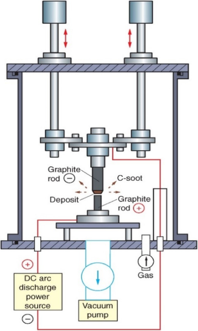
CNT 합성에 사용되는 아크 방전 시스템의 개략도. 이 기술에서는 높은 압력과 온도로 유지되는 금속 반응기 내부에 큰 아크 전류가 흐르면 흑연 전극 중 하나에 나노튜브가 생성됩니다. [79]에서 수정
이 기술은 아크 방전 기술과 유사합니다. 그러나 연속적인 레이저 빔이나 아크 방전 대신에 그림 6[84]과 같이 펄스 레이저를 사용합니다. 레이저 빔은 He, Ar, N2와 같은 불활성 가스가 있는 상태에서 큰 흑연 타겟을 기화합니다. ~ 1200 °C의 석영 관로에서 등. 그런 다음, 기화된 탄소 응축물과 CNT는 반응기의 더 차가운 표면에 자가 조립됩니다[85,86,87,88]. 두 전극이 모두 순수한 흑연으로 만들어진 경우 MWCNT는 ~ 1 nm ~ 2 nm의 내부 직경과 약 10 nm의 외부 직경으로 생성됩니다[89]. 흑연 타겟이 Co, Fe 또는 Ni로 도핑될 때 생성된 침전물은 SWCNT '로프' 또는 번들에서 풍부한 것으로 관찰되었습니다(그림 1e). 생산된 CNT의 수율과 품질은 레이저 특성, 촉매 조성, 성장 온도, 가스 선택 및 압력과 같은 성장 환경에 따라 달라집니다. 이 방법은 고출력 레이저 빔이 필요하기 때문에 비용이 많이 들 수 있습니다. 이 기술의 한 가지 장점은 불순물이 적기 때문에 성장 후 정제가 아크 방전 방식만큼 집중적이지 않다는 것입니다.
<그림>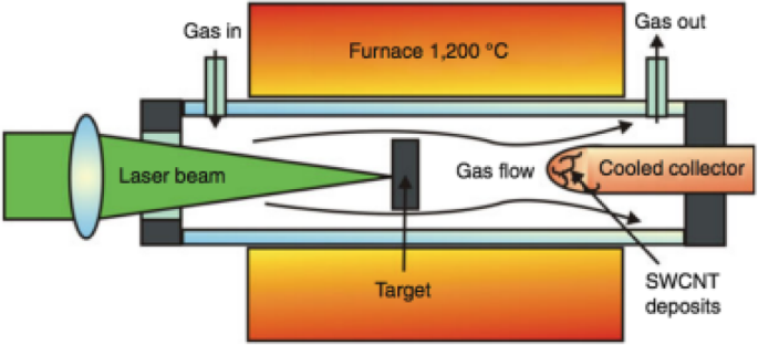
CNT 합성에 사용되는 레이저 절제 시스템의 개략도. 이 기술에서 CNT는 원자로 표면에서 CNT의 자가 조립을 유도하는 흑연 타겟을 기화시키는 레이저 빔의 도움으로 석영 관로에서 생산됩니다. 전극의 유형(순수 흑연 또는 Co, Fe 또는 Ni로 도핑된 흑연)에 따라 형성된 CNT는 단일벽 또는 다중벽일 수 있습니다. [84]에서 수정
화학 기상 증착(CVD)은 탄화수소 증기의 열 분해에 금속 촉매를 사용하기 때문에 일반적으로 촉매 화학 기상 증착(c-CVD)이라고 합니다. 촉매는 CNT의 성장에 매우 중요한 역할을 합니다. 이상적인 촉매는 기질 표면에 단분산되어 있어야 합니다. 또한 반 데르 발스 힘을 통해 기판과 적절하게 상호 작용해야 합니다. 촉매와 기질 사이의 약한 상호작용이 있을 때 SWCNT의 성장 효율이 향상될 수 있다. 고온에서 금속 촉매는 매우 불안정하고 SWCNT의 키랄성 제어 성장은 어려운 작업이 됩니다. 이상적인 촉매는 더 높은 온도에서 우수한 안정성을 제공해야 하며 더 나은 직경 분포로 CNT의 성장을 제어해야 합니다. 촉매 지지체와 촉매 나노입자 사이의 상호작용을 증가시킴으로써 고온에서 직면하는 일부 문제를 제어할 수 있습니다. 탄화수소 공급원은 액체(벤젠 및 알코올), 증기(일산화탄소) 또는 고체 형태(장뇌)일 수 있습니다[79]. 탄화수소의 분해에는 Fe, Co, Ni, Mo와 같은 나노미터 크기의 전이금속 촉매가 일반적으로 사용된다[90,91,92]. 또한 Cu, Au, Ag 및 Pt와 같은 금속 촉매도 일부 연구에서 사용되었습니다[93]. 어떤 경우에는 이러한 금속 촉매가 SiO2,와 같은 촉매 지지체와 혼합됩니다. MgO 및 Al2 O3 탄소 공급원료와 금속 입자를 포함하는 촉매 반응의 표면적을 증가시키기 위해 [94].
사용되는 탄화수소 및 촉매 유형의 선택은 VLS(기상-액체-고체) 또는 VSS(기상-고체-고체) 메커니즘이라고 하는 다양한 성장 메커니즘을 결정합니다. 둘 중 VLS 메커니즘이 널리 사용됩니다. 여기서 촉매 입자는 액체 상태로 탄화수소가 금속 입자에 흡착되어 촉매 분해된다. 다음으로, 탄소는 입자에 용해되어 액체 공융을 형성하고 나중에 과포화 시 관 형태로 침전됩니다[95, 96]. 반면에 VSS 성장 메커니즘은 고체 촉매를 사용합니다[97].
합성 방법은 ~ 600–1200 °C의 온도에서 금속 촉매의 존재 하에 탄화수소 증기의 분해로 시작됩니다[98, 99]. 탄화수소 증기가 금속과 상호 작용하면 탄소와 수소로 분해됩니다. 탄소는 수소 가스가 증발하는 동안 금속에 용해됩니다. 그런 다음, 촉매-기질 상호작용에 기초하여 금속 촉매 상에서 CNT의 성장은 그림 7과 같이 팁-성장 메커니즘 또는 베이스-성장 메커니즘의 형태로 나타난다[100, 101]. 팁-성장 메커니즘 약한 촉매-기질 상호 작용 때문입니다. 여기에서 탄화수소는 금속 상단에서 분해되고 탄소는 금속을 통해 확산되기 시작합니다. CNT는 금속의 기저부에서 성장하기 시작하여 금속의 농도 구배를 기반으로 추가 탄화수소 분해를 위한 충분한 공간이 있을 때까지 계속해서 더 길게 성장합니다. 이 과정에서 금속은 그림 7a와 같이 기판에서 더 멀리 밀려납니다. 염기 성장 메커니즘의 경우 강력한 촉매-기질 상호 작용이 있습니다. 팁 성장 메커니즘과 유사하게 탄화수소는 금속 상단에서 분해되고 탄소는 금속을 통해 확산되기 시작합니다. 그러나 강한 촉매-기질 상호작용으로 인해 금속 입자가 위로 밀려나지 않고 CNT가 그림 7b와 같이 금속 위에서 자라게 된다. 그림 8은 CVD를 통해 성장한 CNT의 예를 보여줍니다[102, 103].
<그림>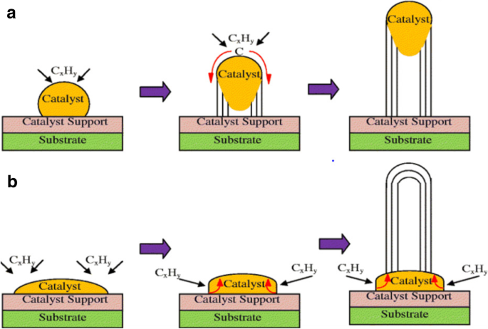
CVD를 사용한 CNT의 다양한 성장 메커니즘([101]에서 수정). 촉매-기질 상호작용을 기반으로 두 가지 유형의 CNT 성장 역학을 볼 수 있습니다. 아 팁 성장 모델:약한 촉매-기질 상호작용으로 탄화수소가 금속의 상단 표면에서 분해되어 탄소가 금속을 통해 아래쪽으로 확산되어 금속 바닥에서 CNT가 자라나는 팁 성장이 관찰됩니다. ㄴ 염기 성장 모델:강한 촉매-기질 상호작용으로 촉매가 염기에 뿌리를 두고 있는 동안 CNT가 기질에서 멀리 떨어진 금속 밖으로 성장하는 염기 성장이 관찰됩니다.
<그림>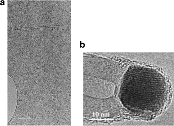
CVD를 통해 성장한 CNT의 TEM 이미지(a ) Fe2를 사용하여 성장한 분리된 SWCNT O3 직경 5 nm의 촉매. 스케일 바는 50 nm와 같습니다. [102]에서 수정. ㄴ 팁 끝에 촉매 입자로 성장한 MWCNT. Adapted from [103]
Size and properties of the catalyst play a significant role in the growth of SWCNTs and MWCNTs using CVD. Smaller particle size (a few nm) leads to the growth of SWCNTs, whereas MWCNTs are formed when the particle size is larger (tens of nm) [1]. The type of hydrocarbons influences the shape of the CNTs produced. For example, methane, acetylene which are linear hydrocarbons, lead to formation of straight hollow CNTs. Cyclic hydrocarbons like benzene and fullerene produce curved CNTs [104].
In addition, the choice of substrate used also plays an important role in the growth of CNTs due to the catalyst–substrate interactions, in turn influencing the yield, quality and aspect ratio of the CNTs produced. Some of the commonly used substrates for growth of CNTs are made of materials like silicon [104], graphite [18], alumina [105, 106] and zeolite [107]. Studies have shown that use of zeolite substrates can result in high yields with narrow diameter distribution and that substrates made of alumina produce high yields of aligned CNTs with high aspect ratio [79, 108].
Along with the catalyst and substrate choices, structural control of individual CNTs is also affected by the temperature and the gas flow rate during the synthesis procedure. Control of gas flow rate during synthesis depends on the type of hydrocarbons used (i.e. gaseous, solid or liquid. An increase in the SW/MWCNT’s diameter is observed with an increase in the synthesis temperature [109]. For example, in case of a Fe–Co–zeolite system with camphor, the ideal temperature for SWCNT growth was reported to be around 900 °C, whereas for MWCNTs, the ideal growth temperature was reported to be 650 °C [100].
Of the three CNT manufacturing techniques discussed in this section, CVD is a widely used technique to manufacture CNTs due to its various advantages such as better controllability over CNT growth, low cost and use of low temperature [79, 105].
Growing CNTs with controllable chirality is an important step in order to utilize them for various applications. This is because the chirality of a CNT determines various properties like electronic band structure and thus, the type of CNTs grown (i.e. metallic vs. semiconducting). Chirality control can be done by direct-controlled growth or post-synthesis separation approaches or by combining these methods [110] and is considered as one of the most challenging aspects in CNT growth [111]. Various parameters such as growth temperature, catalyst and hydrocarbon type influence the chirality of the CNTs. Direct controlled growth methods aim at controlling the chirality by controlling the nucleation process, as it is reported that during the nucleation process, chirality of a SWCNT is fixed [112]. For example, plasma-enhanced CVD (PECVD) has been used for the preferential growth of semiconducting SWCNTs [113]. In addition, semiconducting CNTs were also grown using ST-quartz substrates and methanol precursors [114]. Various growth parameters like type of catalyst, growth temperature and pressure and the source of the hydrocarbons play a significant role in influencing the nucleation which in turn controls the chirality of the tubes grown. Some of the techniques like use of CNT growth templates as seeds (both metal-based and non-metal based), growth initiated by carbon molecular-based precursors and use of nanoparticle-based catalysts have gained a great interest in this field. Some of these are discussed below:
In the first technique we describe, a single (n , 나 )-type SWCNT nanotube sample is cut into smaller pieces (seeds), each of which was aimed to be used as a template for the growth of a longer nanotube using a VLS amplification process (Fig. 9a). The main goal of this method was to grow large quantities of n , 나 -controlled structures. Each seed was polymer-wrapped SWCNT, end-carboxylated and tethered with Fe salts at its ends. During the growth process, Fe salts acted as growth catalysts and use of VLS mechanism aimed at achieving narrow diameter distribution [115]. SWCNTs grown with this method had a diameter similar to the diameter of the growth seed (Fig. 9b–f). However, details about the modifications in chirality of the tubes grown could not be clearly established [116]. In addition, this method also involves the need for complex purification steps due to the presence of metallic particles in the SWCNTs grown, thus affecting the final product’s quality.

아 Growth mechanism of SWCNTs using Fe seeds as growth templates. Adapted from [116]. ㄴ , ㄷ Atomic force microscope (AFM) images and height analysis of SWCNTs before the amplification process. Adapted from [116] and d , f after amplification growth process. Adapted from [116]. White arrows represent the original SWCNT seed location, red arrow indicates the seed position and angle relative to the locator inscription and yellow arrows show the entire length of the amplified nanotube. Adapted from [116]
As an alternative to metal-catalyst-based growth, another technique involved the controlled growth of CNTs by using semiconductor nanoparticles like Si and Ge as the growth templates. In one of these experiments, CNTs were grown using semiconducting nanoparticles (of size 5 nm or smaller), by introducing thermally decomposed carbon atoms from ethanol at 850 °C. However, CNTs grown in this experiment were considered to be of very low quality and low yield as compared to experiments using Fe, Co or Ni as catalysts [117]. Another growth technique was via an open-end growth mechanism, commonly referred as ‘cloning’ (Fig. 10) [118]. Here, the chirality of the SWCNTs was controlled by using open-end SWCNTs as seeds/catalysts without using a separate metal catalyst. Using these seeds, duplicate CNTs were grown on a SiO2 /Si 기판. The total yield reported in this method was ~ 9%, which could be improved to 40% by growing SWCNTs using this method on a quartz substrate [118]. Another technique based on vapor-phase epitaxy was used to grow the SWCNTs with predefined chirality. This method combined CVD and SWCNT separation techniques by using deoxyribonucleic acid (DNA)-separated single chirality SWCNT seeds as the growth templates. These seeds were of very high purity (~ 90%) and C2 H5 OH and CH4 were used as the carbon sources. This experiment showed significant elongation of the SWCNTs grown from a few 100 nm to tens of microns. The total yield produced in this method was very low [110] and some of the studies related to vapor phase epitaxy (VPE)-based growth techniques are ongoing with aims to improve the yield.

아 –ㄷ Schematic diagram showing the growth process of ultra-long SWCNTs using e-beam lithography cut nanotube segments as the template via ‘cloning’ mechanism. Adapted from [118]. d , e SEM and AFM images SWCNTs used for preparing open-end SWCNTs seeds. Adapted from [118]. 에 , 지 SEM and AFM images of short parent SWCNTs segments for the second growth Adapted from [118]. 아 , 나 SEM and AFM images of duplicate SWCNTs continued grown from the SWCNTs. Adapted from [118]
One way to selectively grow chiral SWCNTs is by using silica substrate and Co-Mo catalyst [119]. Nanotubes of (6,5) and (7,5) chirality were obtained in this technique. With proper interaction between the Co and Mo oxides, aggregation of Co nanoparticles at high temperatures could be avoided. In addition, by optimizing the gaseous feed composition, growth and temperature, selectivity of (6,5) nanotubes was improved by ~ 55% [120]. Another approach for the selective growth of (6,5) SWCNTs was demonstrated using Co-Si catalyst and provided narrow distribution chiral SWCNTs [121]. High quality (6,5) tubes have also been grown at 800 °C using atmospheric pressure alcohol CVD on silica-bimetallic CoPt catalysts with narrow chirality distribution by tailoring the catalyst composition [122]. (9,8) SWCNTs were grown with high selectivity using Co nanoparticles and nanoporous Si support (TUD-1) [123]. Recently, (12,6) SWCNTs were synthesized using tungsten-based bimetallic solid alloy catalyst, W6 Co7 , with purity of> 92% (Fig. 11) [124]. This high level of purity was attributed to the W6 Co7 catalyst which has a very high melting point of 2400 °C and provides a potential avenue for the growth of high purity SWCNTs by using nanoparticle catalysts.

Growth of high purity, single chirality (12,6) SWCNTs using tungsten-based bimetallic solid alloy catalyst (W6 Co7 ). These alloy nanoparticles catalyze the CNT growth on SiO2 /Si substrates via ethanol CVD that help in chirality control during CNT growth. Adapted from [124]
Recently, selective growth of semiconducting SWCNT with diameters in the range of 0.8–1.2 nm was reported based on the deactivation process of the catalyst using a technique known as ‘catalyst conditioning process’ [125]. Here, the catalysts favoring the growth of metallic SWCNT are exposed to the catalyst conditioning parameters (oxidative, i.e. water) and reductive (i.e. H2 ) gases prior to the growth process which leads to the deactivation of these catalysts. An inverse relationship between yield and selectivity based on catalyst deactivation was reported in this work.
Evolving methodologies in the field of organic chemistry have enabled the synthesis of various carbon-based precursors that could be used in growing CNTs with controlled chirality. Some of the examples include flat CNT end-caps, three-dimensional CNT end-caps and carbon nanorings [111, 126, 127], which have all been tested and have proved to stimulate CNT growth under controlled environment. However, each of these approaches has some limitations [128].
In one method, in order to yield hemispherical caps, thermal oxidation was used to open fullerndione. However, there were challenges in the synthesis of single chirality CNTs due to the lack of control in the formed hemispherical cap structures [129]. Synthesis of CNTs using carbon nanorings, viewed as sidewall segments without the cap was also developed [126] but the researchers were unable to control the chirality of the as-grown CNT. An alternative technique was developed by other researchers using an organic chemistry approach to synthesize pure molecular seeds of C50 H10 as an end-cap of a (5,5) chirality nanotube [130]. In this method, the researchers demonstrated chirality-controlled synthesis of SWCNTs through VPE elongation that was free of metals (Fig. 12a). Even though the grown nanotubes were well aligned and of high density, in Raman characterization, it was observed that the synthesized SWCNTs were not (5,5) chirality. It was also observed that the as-grown semiconducting nanotubes were of smaller diameters [130]. Around the same time, another method was demonstrated to synthesize single chirality SWCNTs with predetermined chirality by using an end-cap precursor and planar single-crystal metal surface [131]. In this method, the researcher’s custom synthesized a precursor (C96 , H54 ) using organic chemistry approach to yield (6,6) nanotube seed through surface-catalyzed cyclodehydrogenation process (Fig. 12b). Although, Raman characterization using 532 nm laser identified that the synthesized SWCNTs had (6,6) chirality, some researchers argue that 532 nm is not in resonance with (6,6) nanotubes. In their study, they quoted that 532 nm was in resonance with (9,2) or (10,0) chirality nanotubes. Furthermore, few others observed that the splitting of G band is not consistent with initial studies in this area that demonstrated the G band of armchair metallic nanotubes as a single symmetric peak [132, 133]. The researchers have recommended further Raman characterization, STM studies to determine whether the as-grown SWCNTs are of (6,6) chirality. The use of organic chemistry techniques has the potential to be referenced in further development of chirality controlled SWCNT synthesis due to the possibility of large-scale synthesis with higher purity.

아 Structure molecular end-caps used for chirality controlled synthesis of (5,5) SWCNTs through VPE elongation that was free of metals. Adapted from [130]. ㄴ Schematic illustration of a two-step bottom-up synthesis of SWCNTs from molecular end-cap precursors. Singly capped ultrashort (6,6) seeds lead to epitaxial elongation of nanotubes using the carbon atoms originating from the surface-catalysed decomposition of a carbon feedstock gas. Adapted from [110]
Most of the fabrication methods used to grow SWCNTs produce polydisperse CNTs of metallic, semi-metallic and semiconducting properties. This variation is based on the way the graphene sheet is wrapped, denoted by the indices (n, m ) that define the chirality of the tube grown. Steps to control these variations are essential for various applications of SWCNTs as the presence of multiple conductivity types can hinder the device performance. Some of the earlier techniques involved the use of gas-phase etchants like methane plasma [134], water vapor [135], oxygen [136, 129, 137] and hydrogen [134], that would etch metallic particles during the synthesis due to their higher reactivity with the metallic nanotubes, thereby leaving the semiconducting nanotubes behind.
Using floating catalyst chemical vapor deposition (FCCVD) technique with oxygen as an etchant in selective removal of m-SWCNTs, ~ 90% yield containing s-SWCNTs with diameters 1.4–1.8 nm were obtained [137]. However, oxygen can combine with other carbon-based materials due to its strong oxidizing properties during the growth process. Controlling the concentration of oxygen during the growth process is a challenging task. As an alternative, water vapor can be used as an etchant in the CVD technique, as it has a much weaker oxidizing ability. A yield of ~ 97% was reported with this technique [138].
Recent studies have reported the importance of diameter dependence on the etching mechanisms. In one of the studies, m-SWCNTs were selectively etched using methane plasma, followed by annealing. At the end, s-SWCNTs are retained on the growth substrates which were stable at high temperatures [139]. By narrowing the diameter distribution to an optimal range of SWCNT diameter, most of the m-SWCNTs are etched within this range. In another technique, to control the diameter distribution, bimetallic solid alloy catalysts like Fe–W (Iron-tungsten) nanoclusters were used as catalyst precursors due to high-temperature stability of tungsten, which causes the nanoclusters to be stable during the CVD synthesis. Water vapor was used as an etchant during the growth process. A yield of ~ 95% was reported with this technique and the diameter of about 90% of the s-SWCNTs formed on the quartz substrate was reported to be in the range of 2–3.4 nm as shown in Fig. 13 [140]. A similar experiment using Fe nanoparticles as catalysts was performed where the overall yields showed broad distribution of the catalyst particle size due to mobility of Fe nanoparticles, which are usually in liquid state during high-temperature CVD growth [94].

아 Diameter and chirality distributions of the FeW-catalysed SWCNTs under a water vapor concentration of 522 ppm. About 90% of the as-prepared SWCNTs were reported to be in the diameter range of 2.0–3.2 nm adapted from [140]. ㄴ Schematic illustration of the diameter-dependent and electronic-type-dependent etching mechanisms during growth. High selectivity of s-SWNTs could be obtained by controlling the diameter via the Fe-W catalysts. Adapted from [140]
Another technique to grow s-SWCNTs with narrow diameter distribution is using carbon-coated cobalt nanoparticle catalyst (termed as acorn-like catalyst) as shown in Fig. 14. The Co nanoparticle acts as active catalytic phase for SWCNT growth. Carbon coating on the outer end prevents aggregation of Co nanoparticles, a major problem faced by most growth methods that lead to formation of larger particles during SWCNT growth at high temperatures [141]. In this technique, the yield of s-SWCNTs grown was ~ 95% with a very narrow diameter distribution centered at 1.7 nm [138].

Step-by-step description of growth of s-SWCNTs with narrow diameter distribution using carbon-coated Co nanoparticle catalysts. Solvent annealing, use of air plasma followed by thermal treatment produced a yield of ~ 95% s-SWCNTs with diameters of about 1.7 nm. 아 Poly-(styrene-block-4-vinylpyridine) film self-assembled into vertical nanocylinders. ㄴ Formation of phase-separated nanodomains from the vertical nanocylinders and adsorption of K3[Co(CN)6]3 catalysts onto them. ㄷ CoO nanoclusters partially surrounded by a polymer layer. d Co catalyst nanoparticles partially coated with carbon to produce acorn-like bicomponent catalysts. 이 Growth of SWCNTs with a narrow diameter distribution from the partially carbon-coated Co nanoparticles followed by in situ etching of m-SWCNTs. 에 s-SWCNTs with a narrow band-gap distribution. Adapted from [138]
Growth of SWCNTs with controllable diameters is regarded as one of the critical parameters in influencing its electrical, surface functionalization and thermal properties [1]. Properties such as band gap and chirality can be controlled by variations in the diameter of the SWCNTs formed. SWCNTs diameter control may be via their growth using floating catalyst method or from a substrate growth method with catalysts deposited on top or using template growth approach. Of the first two techniques, growth via floating catalyst method offers better control over the diameters of the tubes grown due to limited aggregation as catalysts are not restricted on a single plane of the substrate. Studies have shown diameter control in the range of ~ 1.2 to 2.1 nm using this method [126]. In one of the studies, diameter control was achieved by adding CO2 (which acts as an etching agent to etch tubes with small diameters) with the carbon source into the aerosol CVD reactor. The corresponding transmission electron microscope (TEM) image and the absorption vs. wavelength plot of SWCNTs grown with different CO2 concentrations is shown in Fig. 15 below. Increasing the concentration of CO2 leads to the shift in SWCNT diameters from 1.2 to 1.9 nm [142] as shown in Fig. 15c. Size and properties of the catalyst also play a significant role in the controlling the growth of SWCNTs and MWCNTs. Smaller particle size (a few nm) leads to the growth of SWCNTs, whereas MWCNTs are formed when the particle size is larger (tens of nm) [143]. For example, with Fe catalyst of average diameters of 9 and 13 nm, MWCNTs of average diameter 7 and 12 nm were produced [105].

아 TEM image of SWCNTs grown by adding CO2 along with carbon source. (Inset) shows the TEM image of an individual SWCNT Adapted from [142]. ㄴ Plot showing the absorption vs wavelength of SWCNTs grown with different CO2 농도. Adapted from [142]. ㄷ The corresponding diameter distributions of SWCNT samples with different CO2 농도. Adapted from [142]
Substrate growth method aims at minimizing particle aggregation by increasing catalyst spacing. For example, centrifuging the nanoparticles before deposition via CVD using ferritin catalyst particles leads to a diameter control in the range of. 1.9 to 2.4 nm [144]. Alternatively, by sandwiching Fe between Al2 O3 in a sandwiched catalyst model, SWCNTs with diameters between 0.8 to 1.4 nm were synthesized [145]. However, SWCNTs grown using these techniques were entangled due to large catalyst spacing.
Another way of controlling the diameters of SWCNTs is by using a template-based growth approach [126, 146,147,148]. Use of carbon nanorings (cycloparaphenylenes), representing the shortest sidewall segment of armchair CNTs (Fig. 16) as growth templates and ethanol as a hydrocarbon source, SWCNTs with diameters in the range of 1.2–2.2 nm were grown. Different types of nanorings (based on number of benzene rings in the structure) were used as growth templates. The diameters of SWCNTs grown were similar to the diameter of the carbon nanorings used, thereby providing an avenue for diameter control of SWCNTs using organic chemistry approaches.

아 Schematic of template-based CNT growth using carbon nanorings (cycloparaphenylene) that represent the shortest sidewall segment of armchair CNTs. Adapted from [126]. ㄴ Representation of various carbon nanorings grown using the template-based method and their corresponding diameters in nm. Adapted from [126]
Several methods report the growth of MWCNTs with controlled diameters [149,150,151,152,153,154]. In one of the methods, aligned CNTs with diameters in the range of 20–400 nm and lengths between 0.1 and 50 μm were produced using the plasma-enhanced hot filament CVD method by tuning the catalyst size (Fig. 17a). Another method reported the importance of supply of carbon reactant and the growth temperature in the formation of large diameter nanotubes [105]. Here, the use of an iron nanocluster with diameter of 9 nm, ethylene as the carbon reactant and growth temperature of 900 °C, large diameter nanotubes with two or three walls were produced. Alternatively, arrays of SWCNTs with diameters of ~ 1.5 nm were obtained using lithographically patterned metallic nanoclusters (Fig. 17b).

CVD based growth of CNTs produced using different diameter nanoparticle catalyst. 아 SEM images of CNTs produced with different diameters (250 nm and 20 nm in diameter) using nickel-coated glass substrates. Adapted from [149]. ㄴ AFM images of nanotubes grown using lithographically patterned catalyst and Co nanoparticles with a diameter of ∼ 1.7 nm. Adapted from [150]
Modifications in the growth of CNTs leading to junction-like formations can create nanotube structures like the three-terminal Y-junction that could be used for novel electronic switching devices and transistors [155,156,157,158]. Y-junction nanotubes can be grown by CVD using anodic alumina templates with adjustable stem and branch templates [159, 160] as shown in Fig. 18a. Another method used Ti-doped Fe catalysts in the growth process to produce MWCNTs (~ 90%) branched in the form of a Y-shaped junction on quartz substrates (Fig. 18b) [161].

아 TEM image of a MWCNT Y-junction nanotube grown by CVD using branched nanochannel anodic alumina templates. The grown Y-junctions were reported to be 6 to 10 μm in length with tunable diameters. Adapted from [159]. ㄴ TEM image of MWCNT Y-junction nanotube grown using Ti-doped Fe catalysts. Catalyst present at the junction (shown as A) leads to the formation of the two branches. B shows a Y-junction grown from catalyst particles that attach on the walls of the nanotube. C represents a catalyst nanoparticle that does not lead to further branching. Adapted from [161]
In addition to the above techniques, SWCNT junctions formed via crossing of different CNTs connected via irradiating the junction with electron beam, using scanning electron microscopy (SEM) have also been reported [162, 163]. Here, under the influence of electron beam, hydrocarbons used in the growth process are transformed into amorphous carbon which is then utilized to attach the nanotubes and form mechanical junctions (Fig. 19a, b). In another similar work, various carbon nanotube junctions (Y-, T-shaped) were formed by electron beam welding which induced structural defects in the nanotubes, leading to the joining of tubes by cross-linking of dangling bonds (Fig. 19c, d) [162].

Growth of a MWCNT nanotube junction (a ) before and (b ) after soldering by deposition of amorphous carbon via electron beam irradiation. Adapted from [163]. ㄷ Y-shaped junction formed by electron beam irradiation. Adapted from [162]. d T-shaped nanotube junction formed after irradiating a preformed Y junction. Adapted from [162]
Alternatively, two-terminal SWCNT junctions can be grown in a controlled manner using temperature modulation during the CVD process (Fig. 20) [141]. In this method, by altering the growth temperature, systematic variations in the diameter and chirality of the SWCNTs lead to the formation of SWCNT intramolecular junctions. These junctions were grown at desired locations by increasing the temperature of the substrate locally using infrared light during CVD. It was also observed that increasing the temperature led to a decrease in the diameter of the growing junctions and vice versa, with no change in the catalyst particle present at the growing tip [141].

아 SEM image of a two-terminal SWCNT intramolecular junction formed by varying the temperature during CVD growth from 950 to 900 °C (temperatures are indicated by T1 and T2 ). Adapted from [141]. ㄴ The corresponding shift in the Raman spectra with variations in the temperature. Inset shows the schematic illustrations of SWNT diameter variations with temperature. Adapted from [141]
Understanding CNT sorting methodologies is important as many of the advanced applications, such as FETs and nanoscale sensors, require monodispersed samples with little structural variation [164]. Before CNT sorting can take place, the tubes must be dispersed in a liquid medium (water or organic solvents). Unfortunately, there are certain constraints which may prevent separation in an aqueous dispersion. For example, CNTs have very strong Van der Waals interactions which restrict sorting [87]. There are several well-developed techniques currently being used for the post-growth purification or sorting of tubes. Some of these are discussed below.
One of the techniques, commonly referred to as the density gradient ultracentrifugation (DGU), has been shown to produce a high yield of pure SWCNTs, without much need for chemical treatment of the sample [165, 166]. DGU, which depends entirely on the buoyant density of the CNT, is an isopycnic separation process. The process is achieved by wrapping the SWCNT sample with a surfactant (Fig. 21) [166]. After the grown SWCNTs are mixed with the surfactant, the aqueous dispersion of surfactant-encapsulated tubes is added to the centrifuge tubes, which contains a pre-existing density gradient medium. A strong centrifugal force is then applied, and it causes the surfactant-wrapped SWCNTs to be separated by the movement of SWCNTs to regions of the density gradient medium which match the tubes’ buoyant densities (isopycnic points). The aqueous dispersions of the SWCNTs are produced by using either linear chain surfactants or bile salts. The density gradient medium is usually made of a salt (lithium chloride, cesium chloride, sodium chloride) solution in water. Nonlinear gradients are preferred because they are very sensitive and allow trapping of particles over the entire length of the centrifugal cell. The gradient density and its variation are important to the sorting process wherein, the gradient needs to be set up such that the distance between the tubes and their isopycnic points is minimal. As the density gradient medium responds to the centrifugal force, it leads to steeper gradient over time and hence redistribution of the density profile takes place during centrifugation [167]. After the centrifugation process, the sorted SWCNTS are removed layer by layer using the fractionation process (using piston, upward and downward fractionation methods), which involves extracting quantities of mixtures to different aliquots which vary in composition with respect to the density gradient of the original mixture. Uniform surfactant coverage is important or adsorbed surfactant molecules will begin to aggregate and form clusters along the tube sidewalls, thereby impeding effecting separation of the tubes. To separate metallic and semiconducting tubes, a co-surfactants mixture is used for the ultracentrifugation process. After the semiconducting tubes have been separated, chirality enrichment of tubes is carried out to generate samples that are rich in a certain chirality of tubes, and the resulting semiconducting-SWCNTs-enriched fraction is passed through a dialysis membrane to remove the surfactants from the SWCNT sidewalls [168]. Finally, the tubes are characterized using various optical spectroscopy methods.

아 Illustration of DGU separation of tubes coated with surfactant based on their diameter and metallicity. The near infrared absorption spectra of SWCNTs is also shown. Adapted from [166]. ㄴ Clear separation of SWCNTs by electronic type and the corresponding absorbance spectra for semiconducting SWCNTs (in red) and metallic SWCNTs (in blue) is shown. Adapted from [166]
Another separation technique, referred to as the ion-exchange chromatography (IEX), is based on the ion-exchange processes occurring between a mobile phase and stationary ion-exchange groups (which are bonded to the support material). The IEX separation method is carried out on single-stranded-DNA-wrapped (ssDNA) SWCNTs, which have different electrostatic interactions with an ion exchange column [169, 170]. By selecting the desired sequence from the vast ssDNA library, purification of the specific (n, m) species was possible. With certain ssDNA sequences greatly improving separations between metallic and semiconducting CNTs as well as between semiconducting CNTs of different diameters and electronic band gaps [171]. The IEX process begins by wrapping ssDNA around individual SWCNTs, to form DNA/CNT hybrids. Some of the DNA/CNT hybrids in aqueous dispersions are electrostatically bound to the positively charged anion-exchange resin (stationary phase). As the mobile phase is passed over the hybrid-resin system, and its ionic strength increases, hybrids with the lowest effective charge density elute within the shortest IEX times. Because the hybrids are found in both the stationary and mobile phases, the separation is based on differences in this distribution. There is less electrostatic attraction between metallic hybrids and the IEX resin than between semiconducting hybrids and the IEX resin, thus in a mixture of metallic and semiconducting CNTs of the same diameter, the metallic hybrid will elute from the column first. This method of DNA-wrapped CNTs produced many single-chirality semiconducting CNTs. Figure 22a shows the optical absorption spectra of 12 purified semiconducting SWCNTs along with their structure. This method could also be used for purification of armchair metallic tubes [133, 169]. An alternative approach to sort metallic and semiconducting CNTs is using anion-exchange chromatography technique. Here, single-stranded DNA form stable complexes with CNTs and can effectively disperse them in water. Here, the chosen DNA sequence self-assembles into an ordered structure around an individual nanotube, helping in nanotube formation (Fig. 22b).

Purification of CNTs with defined helicity with the aid of specific DNA sequences using IEX. 아 Absorption spectra of twelve purified semiconducting CNT species along with their (n, m ) structural notations. Adapted from [169]. ㄴ Molecular dynamics model of (8,4) nanotube obtained by rolling a 2D DNA sheet with ATTTATTTATTT strands. Orange color indicates thymine, green color indicates adenine and yellow color shows the backbones. Adapted from [169]. ㄷ , d Chirality separation of SWCNTs using allyl-dextran-based multi-column chromatography. ㄷ Using SDS as a single surfactant, the dispersed SWCNTs were adsorbed on column medium and, upon saturation, the single-chirality tubes are enriched according to its binding affinity towards the column. Adapted from [176]. d Bulk separation of iterative column chromatography to produce single chirality enriched SWCNTs, showing their distinct colors according to their chirality. Adapted from [176]
Gel chromatography, particularly, agarose gel chromatography is a method of separating semiconducting CNTs from metallic CNTs in an mass-spectroscopy mixture using hydrogels [172, 173]. Agarose gel beads are used for mass-spectroscopy separation, owing to their simplicity, affordability, short process time of about 20 min and scalability. The mechanism for gel chromatography follows a few simple steps. First, the SWCNT mixture, containing both metallic and semiconducting CNTs, would be dispersed in an aqueous surfactant solution, such as sodium dodecyl sulfate (SDS). The wrapping and encapsulation of the SDS surfactant molecules around SWCNTs plays a crucial role in the separation mechanism. The interaction between SDS molecules and SWCNTs via ion-dipole forces depends on the pH condition and concentration of SDS molecules. Due to the electrostatic properties of SWCNTs [174], SDS molecules form different types of micellar structures around semiconducting and metallic SWCNTs [172, 175]. On semiconducting CNTs, randomly oriented, flat micellar structures are formed, while for the metallic CNTs, cylindrical micellar structures are formed. This is mainly due to difference in ion-dipole forces between metallic and semiconducting CNTs during their adsorption on agarose gel. These disparate encapsulation mechanisms form the basis of the separation process. After the SWCNT dispersions are formed, they are ultra-centrifuged to remove SWCNT bundles and other impurities, and the SWCNT-surfactant solution is pipetted to be used in the separation process. Next, a separating column is filled with agarose micro-beads suspended in ethanol, after which the column is washed and equilibrated using the surfactant aqueous solution. The agarose-SWCNTs mixture, which is to be separated, is then poured into the column, and the SDS solution is added. This causes a displacement of the SWCNT dispersion along the column. A portion of the SWCNTs (the semiconducting CNTs) are trapped at the top layer of the agarose beads, while the metallic CNTs move to the bottom of column. This movement is related to the encapsulation of the tubes. Because semiconducting SWCNTs are encapsulated by flat randomly oriented SDS micelles, and have less surfactant coverage, there will be an ineffective shielding between the semiconducting SWCNTs and the agarose gel, and thus, a stronger affinity of the semiconducting SWCNTs to the gel. However, the metallic SWCNT walls are surrounded by an ordered high-density cylindrical micellar structure, which causes a steric hindrance between the SWCNTs and the agarose gel. Therefore, the metallic tubes have less affinity to the agarose gel. A schematic of SWCNTs separation based on the chirality of the tubes is shown in Fig. 22c, d [176].
Another technique to separate metal and semiconductor nanotubes is using the technique of dielectrophoresis (DEP). When a particle is placed in an electric field, a lateral force, also known as a dielectric force acts on it [177]. This force can be used to manipulate nanoparticles or cause them to move, and the resulting movement of particles is termed dielectrophoresis [178]. The operating principle of the alternating current (AC) DEP process is based on the fact that metallic and semiconducting CNTs have different dielectric constants. The setup consists of a fabricated microelectrode, fluidic chamber and the SWCNT solution. The DEP force is generated by applying a non-uniform electric field to the setup. Due to the applied electric field, a dipole moment is induced on the SWCNT mixture, and the tubes will move towards the maxima or minima of the electric field depending on their polarity. Under the action of an AC electric field, CNTs in solution will move to the electrodes depending on their surface charge [179,180,181]. The electrodes are typically fabricated using e-beam lithography, which are then attached to a function generator. When an AC electric field originating from the function generator operating at 20 V peak-to-peak voltage and a frequency of 10 MHz is applied, a suspension of ~ 10 μL of SWCNTs is deposited. The metallic nanotubes will attach themselves to the electrodes, while the semiconducting tubes will remain in the suspension (Fig. 23) [182]. This is due to the divergent responses of the different types of CNTs to the electric field. In this technique, direct current (DC) electric field is not usually used as it leads to aggregation of CNTs near one of the electrodes [179]. The applied electric field and deposition time are the crucial parameters which control the CNT deposition yield.

아 Schematic of the experimental setup of the dielectrophoresis of a SWCNT solution using a microelectrode array. The metallic tubes (in black) are deposited on the electrodes and semiconducting tubes are left in suspension (in white). Adapted from [182]. ㄴ Rayleigh scattered dark-field micrograph showing aligned SWCNTs (in green) and the corresponding polarized SWCNTs perpendicular to the electrodes. Adapted from [182]
Gel electrophoresis was developed as an improvement to the AC dielectrophoresis method. This process makes use of the same mechanism as AC electrophoresis but uses agarose gel as a medium. SWCNTs dispersed in an aqueous SDS surfactant are used to fill a gel column and subjected to an electric field. This causes a movement of the m-SWCNTs through the gel medium to the anode while the s-SWCNTs are adsorbed to the gel [177, 178].
Sorting of CNTs can also be done using solution-based conjugated polymers which can be used for selecting pure semiconducting SWCNTs from CNT samples. Here, semiconducting CNTs are wrapped with conjugated polymers, and this technique is considered helpful for selective and large-scale sorting of CNTs [183]. In this method, the SWCNT-polymer mixture is sonicated in an organic solvent for half an hour in order to disperse the SWCNTs. Next, the polymer-wrapped SWCNT solution is centrifuged for about an hour, which results in the sedimentation of m-SWCNTs. Finally, the s-SWCNT supernatant/liquid, which is found lying above the m-SWCNT sediments, is collected for use [183].
In another technique, a gas-phase plasma hydro carbonation reaction is used to selectively etch and gasify metallic nanotubes, retaining the semiconducting nanotubes in near-pristine form [139]. In this method, an array of 98 devices each consisting of ~ 0–3 as-grown SWCNTs grown using CVD were fabricated on an oxide-coated Si substrate. Each SWCNT was of ~ 1–2.8 nm in diameter. These arrays consisted of 55% semiconducting tubes which were non-depletable by the sweeping gate voltage, and about 45% metallic tubes which were depletable with on/off conductance ratio of ≥ 10 3 . These arrays were exposed to methane plasma at 400 °C and then annealed at 600 °C in a quartz tube furnace. Post this, it was observed that the metallic CNTs were selectively removed and the semiconducting tubes were left behind in a greater proportion of about 93%.
Integrating multiple CNTs is essential for the realization of large-scale device applications. This has proved challenging due to the need for precise control and positioning of the fabricated CNTs with respect to other device elements. In this section, we focus on some of the existing techniques that are used in the process of batch level control, fabrication of multiple CNTs and their subsequent integration onto the substrates.
During CVD, a catalyst is often dispersed on the substrate from a solution containing a suspension of the nanoparticles. This is done by spin coating the substrate or by dipping the substrate into the catalyst solution. Alternatively, catalysts can also be deposited on the substrates by evaporation to create thin films. In order to position the catalysts at specific locations, different lithographic techniques like photolithography and microprinting have been reported.
Photolithography is used to pattern the catalyst which leads to growth of CNT thin films after lift-off. In one of the methods, controlled growth of CNTs with diameters of 0.5–1.5 nm was reported using Fe salt as catalyst. In this work, photolithography produced liquid catalyst islands on polymethyl methacrylate (PMMA) and alumina substrates. However, most of the CNTs grown were randomly oriented [184, 185]. Self-assembled masks can also be used to pattern catalysts in solution in order to control the positioning and alignment of nanotubes [186]. Another work reported the controlled growth of CNT thin films in certain regions by catalyst particle patterning using self-assembled monolayers. Here, a thick silicon substrate was thermally oxidized and positive photoresist mesas where CNT thin films were formed were patterned [187]. In a recent work, the growth of SWCNTs with diameters in the range of 0.7 nm to 2.6 nm using Prussian blue analog (PBA)-based bimetallic catalysts was reported [188]. Control on the overall catalyst size and properties was possible by synthesising PBA nanoparticles with narrow size distribution. Silicon wafers coated with an oxide layer were used as substrates. On these, a self-assembled monolayer of silane molecules (having a pyridine group at the ends) was deposited in order for the bond formation with the PBA nanoparticles to occur. Catalyst precursor reduction and the SWCNT growth were done via CVD with CH4 (Fig. 24).

Schematic of the steps followed in the methane CVD growth of SWCNT using PBA-based bimetallic nanoparticle catalysts. In this technique, SWCNTs with diameters in the range of 0.7 nm to 2.6 nm were grown on silicon substrates coated with an oxide layer onto which self-assembled silane molecules were deposited. Adapted from [188]
Nano-imprint lithography (NIL) is another technique for patterning the catalyst [189]. This technique can be used to produce CNTs (in the form of both individual tubes and arrays or forests) with sufficient degree of control over diameters, length and quality [190, 191]. NIL uses silicon molds/stamps with different patterns of nanoscale features to imprint a desired pattern onto a polymer-based thermal resist. After this, required pressure and ultraviolet (UV) light are applied to solidify the polymer resist and form desired circuit patterns. In some cases, temperature can also be applied to the photoresist instead of UV light. Later, the stamp is removed from the resist which leaves behind an imprint of the desired patterns on the substrate. The residual layer of polymer is removed by plasma etching, thereby exposing the substrate onto which the catalyst is deposited. This substrate is loaded into CVD to grow patterns of CNTs. An example of this step-by-step procedure and the corresponding scanning electron microscope (SEM) images of CNTs grown using NIL is shown in Fig. 25 [192, 193].

아 Schematic of steps involved in the growth of CNT arrays using NIL. Adapted from [193]. ㄴ , ㄷ SEM images of CNTs grown using NIL. ㄴ CNTs arranged in a word format reading ‘Nano imprint’. Scale bar equals 20 μm. Adapted from [192]. ㄷ An array of CNTs with 10 μm spacing. Inset shows the tip of an individual MWCNT grown using Ni catalyst. Adapted from [192]
New techniques using nanolithography like nanowriting with nanopipettes [194] and dip-pens [195] help in the growth of CNTs at predetermined locations. For example, in the dip-pen method, the tip of an atomic force microscope (AFM) is usually dipped in an ‘ink’ that can subsequently be transferred to a substrate with nanometer-scale precision. Similarly, nanowriting provides direct and precise control over surface patterning without requiring complex lithographic processing [196].
Controlled production of large-area SWCNT networks can also be done using precise nanometer-scale catalyst patterning resulting in desired alignment of individual SWCNTs on silicon [197]. In this method, the catalysts act as a breadboard that connects the nanotubes with desired alignments. Here, a colloidal mask was used to pattern catalyst nanoparticles using polystyrene spheres that were deposited from liquid suspension and allowed to self-assemble during drying into hexagonal close-packed monolayer regions as shown in Fig. 26.

아 Schematic of steps involved in fabrication of patterned catalyst array on undoped Si substrates using colloidal lithography. The spheres represent polystyrene spheres with a diameter of 450 nm. Adapted from [197]. ㄴ SEM image of the individual SWCNTs connected between catalyst patterned nanoparticle arrays. Adapted from [197]. ㄷ , d AFM image of individual SWCNTs with diameter of ~ 2 nm. Adapted from [197]. Green line shows the d corresponding cross-section. Adapted from [197]
Additionally, catalyst patterning can also be used to control the growth orientation of CNTs during CVD by patterning the catalyst layer on slanted surfaces etched using potassium hydroxide (KOH) as shown in Fig. 27 [198]. In this technique, the catalyst is patterned fully or partially on slanted trenches fabricated via KOH etching. After this, the patterning of a catalyst layer (of 1 nm Fe and 10 nm Al2 O3 ) is carried on the sidewalls using lift-off and e-beam evaporation. Then, CVD is used to grow CNTs with the following conditions; growth was carried out at 775 °C for ~ 5 or 15 min).

Schematic of a catalyst patterning technique which involves the control of growth direction of CNTs by partially patterning the catalyst layer on slanted KOH-etched edges. The corresponding SEM image of CNT pillars grown on the pyramid inside the KOH-etched microchannel is shown. Adapted from [198]
Controlled synthesis of CNTs can be achieved by growing them on the SiO2 /Si substrates in electric fields established across patterned metal electrodes [199]. In this technique, Si wafers were used with thermally grown SiO2 as substrates. Molybdenum (Mo) metal electrodes with a gap of 10 mm were used to establish electric fields on the substrates. Then, the desired catalyst was patterned on top of the two opposing Mo electrodes leading to the growth of aligned SWCNTs across the gap between the electrodes in the direction of the applied electric field. Figure 28 [199] shows the AFM images of randomly grown nanotubes in the absence of an electric field and aligned nanotubes grown in the presence of an electric field.

AFM images of CNTs grown using CVD technique between two Mo electrodes which are shown on top and bottom of the images. 아 Randomly grown CNTs in the absence of an electric field. Adapted from [199]. ㄴ Aligned grown in the presence of an electric field (a bias voltage of 10 V bias applied between the electrodes having a gap of 10 μm). Adapted from [199]
Another method of controlling the growth of CNTs is based on rapid heating (900 °C for 10 min) of catalyst nanoparticles (Fe/Mo) in the presence of feeding gas (CO/H2 ) [200,201,202]. SWCNTs were grown parallel to the direction of feeding gas flow. This work reported directional control of the CNTs grown by positioning the substrate based on the gas flow direction. The location and length of SWCNTs was controlled by using photolithography to deposit the catalysts. This method produced ultra-long, well-aligned and well-isolated SWCNTs with length of few mm (Fig. 29) in contrast to an earlier work that reported that long SWCNTs (in the range of mm) either bend or form loops [203]. Here, the growth of long and straight SWCNTs was attributed to the above described growth process also termed as a kite-based growth mechanism [201].

(a의 SEM 이미지 ) catalyst pattern seen on oxide coated Si wafer prior to the growth of SWCNTs. Adapted from [202]. ㄴ Long, well-oriented SWCNTs grown using fast-heating growth process with Fe/Mo nanoparticles, CO/H2 900 °C for 10 min. Inset shows the magnified image of the SWCNT arrays formed. Adapted from [202]. ㄷ Well aligned arrays of SWCNTs (~ 5 SWCNTs μm −1 ) formed by CVD growth on a ST-cut quartz substrate. Adapted from [207]. d AFM image of aligned SWCNTs grown on r-plane (1 1 0 2) crystalline surfaces of sapphire. Adapted from [206]
Large scale, highly aligned SWCNTs arrays can also be grown by interactions between SWCNTs and the substrate [204,205,206,207] using atomic arrangement-programmed growth. Highly aligned SWCNTs could also be grown using Y-cut single-crystal quartz or ST-cut quartz substrates using CVD of methane at 900 °C and Fe catalyst. As shown in Fig. 29c, SWCNTs with diameters of 1 ± 0.5 nm were grown on quartz using this technique. In this method, SWCNTs were synthesized using CVD of methane at 900 °C with Fe clusters that were dispersed on the sapphire substrates. Alternatively, use of a-plane and r-plane sapphire (Al2 O3 ) substrates led to guided growth along specific lattice directions due to the attractive interactions between nanotubes and Al atoms that are oriented in specific crystalline directions on the substrates (Fig. 29d).
CNT forests (or CNT arrays) are arrays of vertically aligned CNTs that offer applications in the field of sensors [208], gecko tapes [209], strong fibers [210] and electrical interconnects due to their ability to carry high current densities of ~ 10 8 A cm −1 [211, 212]. Various techniques such as use of plasma CVD, nanopatterning and flying carpets have been proposed as means of growing CNT forests [210, 213, 214]. Of these, CVD is regarded as one of the most efficient techniques to grow vertically aligned CNTs. Precise diameter control of CNT forests using pre-growth conditioning and catalyst engineering is one of the crucial parameters that influences its use in various applications [215,216,217]. In addition, control of number of layers and length of the tubes grown is also essential [218].
Growth of aligned MWCNT forests with diameters of ~ 8–15 nm was achieved using CVD in a quartz tube. Here, a Si wafer was used as a substrate, onto which a 5-nm-thick film of Fe (acting as a catalyst) was deposited using e-beam evaporation [219]. An alternate method for the fabrication of a closely packed MWCNT forest was reported using a multi-step growth method based on plasma-induced CVD technique [220]. The growth mechanism involves the following steps. First, very high-density plasma-induced catalytic nanoparticles were formed from a pre-deposited catalytic thin film. It was observed that these catalytic nanoparticles tend to aggregate at higher temperatures. In order to avoid this, the CNT nucleation process (immobilization procedure of catalytic nanoparticles) was performed and showed minimal aggregation of nanoparticles covered with graphitic carbon film. Finally, closely packed MWCNT forests were grown at a temperature of 450 °C (Fig. 30) [221, 223].

아 Critical stages of CNT forest growth from a pre-deposited catalytic thin film using the multi-step plasma-induced CVD technique:formation of high-density plasma-induced nanoparticles, nucleation, and CNT forest formation. Adapted from [221]. ㄴ SEM image of the closely-packed MWCNT forest grown using plasma-induced CVD. Adapted from [222]
The direction of alignment of CNTs with respect to the substrate plays a crucial role in controlling the properties of CNTs grown. CNTs aligned vertically (i.e. perpendicular) to the substrate can be produced using porous silicon substrates with a catalyst patterned by electron-beam evaporation through shadow masks to produce MWCNT blocks. Another technique to produce these CNTs is using water-assisted CVD that produced SWCNT arrays in the order of few millimeters [135]. Here, large-scale production of dense CNT forests was reported to be possible with the help of CVD synthesis where the performance and lifetime of the catalysts was enhanced with the help of water. SWCNTs in the form of well-ordered pillars with a height of ~ 1 mm were grown from lithographically patterned catalyst islands as shown in Fig. 31 below. Alternatively, large-scale production of vertically aligned SWCNT forests is also possible using the oxygen-assisted CVD method. It was reported that the hydrogen species present during hydrocarbon CVD growth method may cause difficulties in the formation of new SWCNTs and can also potentially etch preformed SWCNTs. The introduction of oxygen during the growth process provides great control over the carbon and hydrogen ratio which is responsible for the growth of vertically aligned SWCNTs [223]. More recently, it was also shown that SWCNT forests could be grown using thermal CVD without a rectated etchant gas [224].

아 , b SEM images of SWCNT forests grown using water assisted CVD. 아 SWCNT cylindrical pillars with 150 μm radius and ~ 1 mm height. Insert shows the root of a pillar. Adapted from [135]. ㄴ SWCNT sheets of 10 μm thickness. Adapted from [135]. ㄷ High-resolution TEM image of the SWCNTs grown using this method. Adapted from [135]
Another technique involves the fabrication of the CNTs within the pores or channels of a nanoporous template [160, 225, 226]. The commonly used templates are track-etch membranes, porous alumina (AAO) templates as well as various other nanoporous structures. Template-based synthesis allows the preparation of nanomaterials with a desired shape. A template is basically a structure in which the CNT networks form. Once the template is removed, it exposes a filled cavity with features similar to those of the template. After deposition, the nanotubes may be allowed to remain inside the pores of the templates, or they can be collected as a group of free nanoparticles. The template-based deposition process commonly makes use of CVD techniques, in which hydrocarbon precursors like pyrene and ethylene are exposed to elevated temperatures inside alumina templates. As the thermal deposition of the gas occurs over the entire surface of the pores, this method offers considerable control over the length and diameter of the tubes. One example of the growth of highly ordered arrays of parallel CNTs inside a hexagonally close-packed nanochannel alumina template is described below. At first, the anodization of high purity alumina was carried out, and led to the creation of a nanochannel alumina template made up of hexagonal array of channels with a diameter of 32 nm and length of 6 μm. Next, a small amount of catalyst (Co) was deposited electrochemically into the bottom of the template channels. By heating these templates at 600 °C for 4–5 h in a tube furnace in the presence of CO, then in a mixture of acetylene in nitrogen at 650 °C for 2 h, growth of highly ordered array of nanotubes was observed (Fig. 32) [160, 227]. Periodic array of nanotubes with diameters ranging from 10 nm to several hundred nm were grown by pyrolysis of acetylene on Co at a temperature of 650 °C.

아 Mechanism of growth of highly-ordered arrays of parallel CNTs using nanochannel anodic alumina templates. The process begins with the anodization of high-purity aluminum on the substrate. By varying the anodization conditions, hexagonal close-packed arrays of varying diameters, densities and lengths can be formed. Adapted from [227]. ㄴ SEM image of the resulting hexagonally ordered array of CNTs fabricated using the method in (a ). Adapted from [227]
Another method in the growth of SWCNT forests, involves the introduction of gas shower system to deliver water vapor and carbon source gas from the top of the forests, rather than traditional way of delivering from the side. This method enables parallel flow of water vapor and carbon source gas to the CNTs within the forest. This technique enables mass production of CNT forests with increased growth yield, height, carbon efficiency and scalability for large area growth [214, 228].
Fabrication and assembly of CNTs on a macroscale is of utmost importance in order to enhance its practical applications [179]. A commonly reported technique is using spin coating. This process of fabricating CNT films involves depositing droplets of CNT-based suspensions at the center of a substrate and then spinning the substrate to a very high velocity such that the CNT dispersion spreads out on the surface of the substrate, forming a thin film (Fig. 33a) [229, 230]. This process is due to the centrifugal force on the CNT dispersion. The thickness of the film depends on the viscosity of the dispersion, angular speed, spin time and the concentration of CNTs. Before the CNT dispersion is formed, it is important to overcome the Van der Waals forces between the tubes, else they will tend to aggregate and form clumps on the film. Amphiphilic surfactants are usually added to enhance the dispersibility of the tubes; conventional surfactant will not suffice because there is a strong charge repulsion between the CNT complexes and the surfactant, which prohibits the deposition of CNTs onto the substrate. Additionally, high-power ultra-sonication or strong-acid treatment is usually performed on the tubes. After the CNT film is deposited, the surfactant is usually either washed off or vaporized from the surface of the substrate. Spin coating is not applicable for large substrates because they cannot be spun at a sufficiently high rate to form an even layer. Additionally, the process lacks material efficiency as a lot of the material is flung off during spinning [229]. Alternatively, electrophoresis process can also be used for the film deposition of CNTs [231]. Some of the other relevant techniques include using composites [232], foams [233], yarns [210] and aerogels [234] as discussed below.

아 Schematic of spin coating process for the fabrication of thin film of CNTs. Adapted from [230]. The corresponding SEM images of the SWCNT film prepared by single deposition of spin coating the substrate with CNT solution in an organic solvent called quinquethiophene-terminated poly (ethylene glycol). Adapted from [229]. ㄴ A schematic of a CNT-polymer composite fabrication via solution-based processing. Adapted from [232]
Due to the various properties that CNT’s exhibit, especially being superior in stiffness and strength, they can be widely used in structural applications. Furthermore, researchers are showing increased interest in tapping CNT’s properties by fabricating them into a polymer matrix. Some of the commonly used CNT-based polymer composites are made up of polystyrene, ultra-high molecular weight polyethylene (UHMWPE), PMMA, epoxy and phenolic resin [62, 235,236,237]. Various techniques have been proposed for fabricating CNT-polymer composites based on the material combinations used. Some of the common methods like solution casting, melt mixing and in-situ polymerization are discussed below.
Solution casting, also referred as solvent casting, facilitates CNT dispersion, where CNTs are suspended in the desirable polymer solution via magnetic stirring or sonication (energetic agitation process). The solvent is then allowed to evaporate to produce CNT-polymer composites. Polymers such as polyvinyl alcohol (PVA) [238], PMMA [239] and epoxy [236] have been used in this method. One such manufacturing technique is shown in Fig. 33. Here, PVA/CNT composite fibers of ~ 50 μm diameter were synthesized using the following steps. First, CNTs were dispersed in ethanol, then a PVA-coated polyester strip was dipped in a solution containing the CNT mixture. Then, the CNT-coated PVA on the polyethylene terephthalate (PET) strip were delaminated. Finally, this delaminated layer was stretched and twisted to form a composite fiber (Fig. 33a). Studies involving different solutions and methods have demonstrated that the selection of solvent for nanotube dispersion had an influence on the properties of synthesized nanocomposites and the type of solvent is dependent on the solubility of polymer in it [240]. A major shortcoming of this method is that the nanotubes may agglomerate if the solvent evaporation process is slow. This may be mitigated by increasing the rate of evaporation [241]. This leads to inhomogeneous distribution of CNT’s in the polymer matrix [242].
Another commonly used method for the fabrication of CNT-polymer nanocomposites is called melt mixing. It is mostly used for manufacturing of thermoplastics and thermistors. Thermoplastic polymers melt/soften when heated to high temperatures thus making them less viscous. This causes the substrate to be less viscous and the need for high shear forces to disrupt the nanotubes bundle. In this method, composites of various polymers (such as polystyrene and polypropylene) are formed with CNTs. To start with, the selected polymers are mixed with nanotubes in a high sheer mixer. Post this, composite films are formed using compression molding [6]. Further studies in this area has enabled different techniques such as extrusion, compression molding, injection molding, etc. for fabricating samples of various shapes [6, 243, 244].
Recently, melt-mixing method was used in the manufacturing of positive temperature coefficient (PTC) thermistors using CNTs as conductive fillers in high-density polyethylene (HDPE) composites. Traditional PTCs manufactured using carbon black (CB) filled high-density polyethylene composites suffer from disadvantages like low thermal stability and poor processability. Use of CNTs in the manufacturing process can help in overcoming these challenges as the CNT-based thermistors showed ~ 129% increase in hold current and hold voltage, in comparison with the CB-filled composites [245]. These CNT/HDPE microstructure composites were prepared by melt-mixing, hot-pressing and packaging methods as shown in Fig. 34a. CNT/HDPE composites showed a decrease in electrical resistivity with an increase in the CNT loading. Figure 34b shows a comparison of current vs time plot obtained for CNT/HDPE and CB/HDPE thermistors.

아 Schematic of the fabrication of CNT/HDPE thermistors using melt mixing. The process consists of melt-mixing, hot-pressing and packaging. Adapted from [245]. ㄴ Graph comparing the current vs time plots of CNT/HDPE and CB/HDPE thermistors. The comparison of the current decay between the CNT/HDPE and CB/HDPE thermistors with the same resistances under peak applied voltages shows a quick response of current delay of the CNT/HDPE thermistors. Adapted from [245]
CNTs can also be fabricated with monomers or polymers of higher molecular weight using in-situ polymerization. In general, this method can be used in the fabrication of almost any polymer composite with CNT to polymer matrix that is either covalently or non-covalently bounded [246, 247]. In addition, this method makes the grafting of larger polymer molecules to the walls of CNT possible. This enables the fabrication using insoluble and thermally unstable polymers that cannot be achieved by solution or melt processing. A stronger interaction of CNTs with polymers during the growth stage due to π-bonding was observed in this technique [248]. One such schematic of fabrication of CNTs using in-situ polymerization is shown below in Fig. 35 [249].

Schematic of formation of SWCNT/P3HT/PPy or SWCNT/P3HT/PEDOT conductive films and fibers using in-situ polymerization. The SWCNT/P3HT monomer dispersions were prepared and then coated onto a glass slide to form a film or extruded from a syringe to form fibers. Adapted from [249]
Many other lesser known methods to fabricate nanocomposites have also been proposed such as twin screw pulverization [250], latex fabrication [251], coagulation spinning [252] and electrophoretic deposition [253].
Three-dimensional porous networks made of polymers and CNTs have a great potential to be used in various applications like energy storage [254] and sensing [255]. Here, CNTs are used as modifiers into structures made of different porous materials like carbonaceous aerogels, foams and sponges [219, 234, 256]. Fabrication of CNT foams and aerogels can be done using several techniques like c-CVD, phase separations, polymerization reactions, etc. Creation of CNT foams and aerogels can be done using a bottom-up method consisting of phase separations induced by thermal phase transition. Here, a three-dimensional (3D) network of CNTs is initially formed in a solution, post which the liquid part is removed without disturbing this network. This technique is commonly referred as freezing as it involves a solid-liquid phase separation process. However, it was reported that CNTs grown using the various freeze-drying techniques lead to agglomerations [257].
Another technique of CNT aerogel formation is using a gas-liquid phase separation process, commonly referred to as foaming as shown in Fig. 36 [258]. Fabrication of CNT foams with controlled pore structures using this foaming process can be done using PVA, polystyrene, polyurethane, etc. [259, 260] An alternate route to the fabrication of CNT foams is using CVD, wherein, by controlling the growth parameters like type of catalyst and source of carbon, vertically aligned CNT array foams could be formed [233, 260]. Recently, aligned CNT foam structures of desired size were fabricated by stacking sheets of CNTs and infiltrating the stacked sheet assembly with pyrolytic carbon (PyC) [233]. Here, vertically aligned MWCNTs were grown using CVD technique with FeCl2 as catalyst and acetylene as the carbon precursor. These aligned CNTs were drawn from arrays and collected around two rotating parallel glass rods in order to have less compacted macro-porous structures. The CNT foams were then coated with 20 to 100 cycles of alumina buffer layers (that pins the catalyst particles on the surface of nanotubes) to help in the formation of secondary CNTs leading to creation of junctions, or branched CNT networks [260, 261]. In this method, prior to CVD, a buffer layer made of Al2 O3 is deposited onto the porous structure to promote secondary CNT growth (in the form of straight CNTs or coiled-CNTs) at the surface of the primary nanotubes and within the pores of the CNT foams [261].

CNT foam formation using various techniques. The figure depicts various phase separation processes being performed on a CNT suspension to produce the CNT foam. The phase separation process is usually done via a gas-liquid phase separation or a solid-liquid phase separation as shown in the figure. Adapted from [258]
MWCNTs shaped into yarns have potential to be used in multifunctional applications like artificial muscles and actuators, in electronic textiles and as fiber-based supercapacitors [219]. Electromechanical actuators formed using sheets of SWCNTs (as electrolyte-filled electrodes of a super capacitor) are reported to have shown higher stresses than natural muscle. Like natural muscles, the macroscopic actuators are assemblies of billions of individual nanoscale actuators and are shown to have a great potential in various applications [39, 262, 263]. In addition, by twisting CNTs from a MWCNT forest, CNT yarns could be formed [219, 264]. Here, MWCNTs with a diameter of ~ 10 nm were drawn from a MWCNT forests (grown using CVD by using Fe catalyst) and twisted with a motor running a variable speed of ~ 2000 rpm [219]. This twisting causes the MWCNTs to form small individual bundles consisting of few CNTs. Further, by allowing the twisted yarns to relax (untwist in an opposite twist direction), knitted and knotted yarns were formed (Fig. 37a–c) [265,266,267]. Alternatively, MWCNT yarns could be synthesized from aerogels during CVD [268]. MWCNTs can also be drawn into sheets from MWCNT forests synthesized using CVD with ~ 3 nm iron film as a catalyst and acetylene or ethylene as carbon source [269]. These sheets were formed as a highly anisotropic electronically conducting aerogels that could be drawn into sheets with ~ 50 nm thickness as shown in Fig. 37d [270].

SEM and optical images of CNT yarns. 아 SEM image of a part of CNT yarn from the nanotube forest being drawn and twisted. Dry spinning of the CNT yarns from the forests (vertically grown CNT array) is shown. Adapted from [266]. ㄴ SEM image of a knotted CNT yarn. Adapted from [265]. ㄷ Optical image of a MWCNT knitted yarn, with a glass rod through the center. The average diameter of the MWCNT knitted yarn was measured to be 34.09 ± 2.86 μm. Adapted from [267]. d SEM image of MWCNTs in a forest being drawn into a sheet. Adapted from [270]
Recently, electrically conducting 3D fabrics made from hybrid Spandex (SPX)–MWCNT yarns showed excellent stretchable properties with a potential to be used as artificial muscles (Fig. 38). They were fabricated in a knitting machine into which a CNT aerogel sheet drawn from CNT forest, wrapped around continuous supply of SPX filament was fed. These fabrics exhibited breaking strains of 600% to 900%, tensile strengths in the range 75 to 86 MPa and an approximate resistance of 3.0 kΩ m −1 [271]. They offer unique advantages such as large tensile actuation, high repeatability, scalability and stretchability due to which they can be used in various applications like medical sensors/devices and smart clothing.

SEM image of CNT/SPX8 knitted textile and the corresponding mechanical properties. 아 SEM image of CNT/SPX8 knitted textile. Adapted from [271]. ㄴ Stress–strain curves of the CNT textile material. Adapted from [271]. ㄷ Strain versus time for this textile, stretched for 1000 cycles at 0.2 Hz. Adapted from [271]
Most methods of CNT mass production result in randomly oriented CNT bundles. The placement and alignment of the tubes can either be done while they are being grown or after they have been grown. In the former, the CNTs are grown in a given direction and position within the substrate or normal to it, while in the post-growth method, the tubes are first isolated in a dispersion and then the dispersed CNTs are aligned and selectively positioned in a certain direction by applying external forces. Various methods have been used for aligning and placement of CNTs on substrates, as discussed below.
Photolithography has been successfully used to prepattern either catalysts or substrates for site-selective growth of CNTs. In such a case, the photolithography setup consists of a substrate (glass), a patterned resist and a photomask. The process involves the following steps; first, direct photolithographic patterning is performed on the metal-containing photoresist. Next, metal oxides are heated and then reduced by hydrogenation to patterned metal nanoparticles, which act as catalysts from which aligned CNTs are grown, via the hydrocarbon pyrolysis of FePc (Fig. 39a, b) [272]. Alternatively, catalyst patterning using photolithography can be done by creating a template with desired patterns of photoresist, followed by molding of PET stamps which are used in transfer printing of CNTs. However, this technique suffers from certain limitations which include not having the necessary resolution to grow nanometer-scale patterns. In addition, growth of CNTs may be hindered/affected due to contamination that may be introduced through these masks [195].

아 Schematic flow diagram of micropattern formation of vertically aligned MWCNT arrays by direct photolithography process. Adapted from [272]. ㄴ SEM images of patterned films of vertically aligned MWCNT arrays formed by the pyrolysis of FePc onto a photolithographically patterned quartz substrate. The resolution of the figure is in the micrometer scale. Adapted from [272]. ㄷ Step-by-step illustration of transfer printing of SWCNTs onto various substrates by contact stamping. Adapted from [273]
Currently, most nanoelectronics devices are being made on flat, rigid, smooth surfaces. This poses a problem because future nanoelectronics applications will require for nanomaterials to be placed on flexible substrates, such as plastic, or nonplanar materials. Due to this, methods such as transfer printing, which allow for the fabrication of a device on a conventional substrate and then transfer-printing of the entire working device onto target substrates, are being developed [273, 274]. This precludes the need for performing harsh synthesis and fabrication methods on the target substrate. The mechanism for transfer printing CNTs is as follows; first, the tubes are stabilized by mixing them with surfactant molecules, next the surfactant-stabilized CNTs are deposited on a variety of substrates from the solution. The most common process for the deposition of the tubes with wide area coverage is based on controlled flocculation. The controlled flocculation approach uses a spinning mechanism, in which the suspension of tubes and a solvent (methanol) are applied at the same time, to a spinning substrate. The methanol or any other hydrophilic solvent displaces the surfactant from the nanotubes, by bonding to them thereby causing the tubes to precipitate from the solution, to the edges of the substrate where they are deposited on a high-resolution polydimethylsiloxane (PDMS) stamp. The tubes form thick films on the PDMS stamps, and the stamp can be pressed on the target substrate to transfer the tube patterns from the raised regions of the stamp (Fig. 39c) [273]. One problem with this technique is the requirement to pattern the stamps each time based on the design [275].
Patterning in thin film CNTFET channels can be achieved with an inexpensive solution-based self-assembled colloidal mask that leads to devices with large on/off ratios while maintaining carrier mobility and sub-threshold performance. By guiding SWCNT thin film formation, the colloidal mask approach allows an ordered nanoscale CNT network with more consistent and accessible channel surface area resulting in patterned thin film FET channels whose structure and properties can be tuned for different applications (such as sensors). In one of the template-based deposition techniques, the patterned SWCNT thin films were fabricated using colloidal lithography [241]. This method employed a liquid-based self-assembly of colloidal sphere monolayers as masks to create ordered nanoscale arrays and films. Here, heavily doped silicon wafers with ~ 100-nm-thick SiO2 layer was used as a substrate and patterning of Au/Ti source-drain electrodes with ~ 40 nm thickness and 1–3 μm spacing on the surface of wafer was carried using photolithography. SWCNT powder (1.2–1.5 nm diameter and 2–5 μm length) was dispersed in chloroform with SDS surfactant to form aqueous suspensions, which was mixed with an aqueous suspension of silica or polystyrene colloidal spheres to form patterned nanotube networks. The overall process flow for patterning the SWCNT thin films and the corresponding results are illustrated in Fig. 40a–c.

아 Schematic of fabrication process for patterned CNTFET networks. ㄴ Optical microscope image of patterned electrode substrates after self-assembled colloidal mask assembly. ㄷ SEM image of interconnected nanotube ring patterns formed during the self-assembly process and gate voltage-dependent I -V characteristics of resulting CNTFET. The center to center distance of the circles is around 500 nm. (Inset) shows the corresponding magnified view of the interconnected nanotube ring patterns. [Y. Chen and C. Papadopoulos, unpublished results]
Another technique to control the placement, alignment and spacing of CNTs is achieved using DNA-origami structures [276,277,278]. Here, various geometrical shaped (L-, T-, Y-, rectangular, triangular, etc.) nanotube structures are formed on DNA-origami templates using self-assembly process (Fig. 41), where the CNTs were organized into several patterns, with control over the inter-tube angles. In one of the techniques, CNTs solubilized by wrapping with ssDNA reacted with the DNA origami constructs forming linear arrays of ssDNA that lead to immobilization of the CNTs onto the DNA origami scaffold. This was due to the strong π–π interaction existing between the bases of ssDNA and CNTs. SWCNTs with lengths ranging from ~ 92 ± 24 nm (termed as short SWCNTs) and ~ 314 ± 249 nm (termed as long SWCNTs) were obtained in this work [276].

Schematics of a rectangular DNA-origami. Adapted from [276]. ㄴ , ㄷ Site-specific immobilization of ssDNA-wrapped short and long CNTs onto the single rectangular DNA-origami scaffold. Adapted from [276]. d AFM images of DNA origami-nanotubes formed using self-assembly showing CNTs aligned at the edges. Adapted from [276]. 이 AFM images of DNA origami-nanotubes formed using self-assembly showing two single rectangular DNA-origamis aligning two long 6,5-SWCNTs. Adapted from [276]. 에 Cross-shaped SWCNTs. Scale bar equals 100 nm. Adapted from [276]
Most solution-based alignment or deposition methods of CNTs require the formation of CNT films from CNT suspensions. As such, there’s a need to form uniform dispersions of CNTs in a solvent. A challenge that is commonly encountered in dispersing CNTs is overcoming the strong inter-tube interaction of CNTs, which is attributed to van der Waals forces. When CNTs are placed in a solvent, they usually bundle together. This attractive force of the CNTs is usually overcome by binding the CNT walls to surfactant molecules (surfactant wrapping) to form stable solutions of CNTs. As such, these van der Waals forces are a major consideration when using solution-based methods for aligning CNTs [230]. Some of the solution-based alignment techniques are discussed below.
Inkjet printing is a precise method of patterning, and therefore, post-printing steps are not needed. This technique is advantageous because it does not require the use of a prefabricated template, thereby allowing for rapid printing at a low cost [279, 280]. Additionally, it is valuable because many layers of ink can be printed on top of one another. The carbon nanotube ink is prepared following certain steps; first, sonication is used to disperse the CNTs within the liquid. After dispersing the CNTs, the ink is centrifuged several times to separate the well-dispersed CNTs from the bundles, which could clog the printer nozzle. Next the supernatant is collected and filtered severally to remove any remaining CNT bundles. After the ink has been successfully produced, it is loaded into an inkjet cartridge and ready to be used for printing on substrates like glass and polymers.
Consumer inkjet printers are of two types; continuous and drop-on-demand. The former supplies a continuous stream of ink droplets, which are charged once they leave the nozzle, and are then deflected by voltage plates, such that the applied voltage determines if the droplet will be deposited on the substrate, while the drop-on-demand printer functions in a different manner, in that, the printer only ejects ink when required [279]. Carbon nanotube inkjet printing has been successfully used to deposit MWCNTs and SWCNTs. It has also been used to fabricate transistors, sensors and electroluminescent devices. The process is a useful development in electronics because it allows direct printing of the CNTs to make a pattern or a circuit on a suitable substrate, thereby enabling us to control the transparency and resistance of the printed patterns (Fig. 42a) [281]. In order to produce uniform networks of CNTs by inkjet printing, the jetting conditions need to be properly tuned to generate correctly directed droplets. Another important consideration is the temperature of the substrate. The substrates need to be heated in order to reduce the drying time for the printed CNT solution. For manufacturing purposes, quick drying of the dropped ink is desirable. However, the temperature should not be too high as it would cause the droplet to evaporate once it is released from the nozzle. A constraint in using this process is the difficulty of dispersing nanomaterials within the ink as CNTs typically bundle together in a solvent, due to their attractive van der Waals forces. The bundling of tubes needs to be prevented as it could cause clogging of the inkjet nozzle [279].

아 Optical image of a CNT-based circuit on polyimide wrapped around a test tube. The circuit was fabricated using CNT inkjet printing. Adapted from [281]. ㄴ Schematic of the Langmuir-Blodgett (LB) process for the fabrication of films. The LB process is either performed using the b vertical dipping method or c horizontal lifting method. Adapted from [283]
Alternatively, spray-coating involves spraying CNTs dispersed in a suspension on a heated substrate such that every sprayed droplet undergoes pyrolytic decomposition when it reaches the hot substrate surface thereby forming a thin layer of CNTs film [282]. CNT films can be spray deposited on glass before being transferred to a flexible substrate or they could be directly sprayed onto the flexible substrate. Before the spraying of the CNTs can take place, the solution has to be prepared. First, CNTs in powdered form are dispersed into a solvent via sonication. The CNTs are usually either dispersed in an organic solvent or in a surfactant-based aqueous dispersion. Surfactant-based dispersion using SDS or carboxymethyl cellulose (CMC) is usually preferred because the surfactants can be rinsed off after the film is deposited, as these surfactants are soluble in water. The surfactant is first dissolved in water to form an aqueous solution, to which the CNTs are later added. This forms a surfactant based aqueous CNT solution. Sonication of the surfactant-based solution is then performed to evenly disperse the CNTs. Finally, the solution is centrifuged, and the supernatant is taken from the top to be used for deposition. Before spray deposition of the CNTs can occur, the substrate surface has to be treated and cleaned using solvents like acetone and isopropanol, followed by plasma cleaning. After treatment of the substrate, the colloidal suspension of CNTs is sprayed through an air atomizing spray gun, onto a heated substrate. The dispersing fluid (in this case, the surfactant) then evaporates due to the heating of the substrate to leave behind a uniform coating or layer of CNTs.
CNT films can also be produced using the Langmuir-Blodgett (LB) technique, in which a substrate is dipped in a solution containing well-dispersed CNTs, and then slowly pulled out either by horizontal lifting or by vertical dipping method as shown in Fig. 42b, c [283]. This technique produces a thin layer of CNTs aligned in the dipping direction on the substrate. The thickness of the CNT film is dependent on the concentration of CNTs in the solution, the pulling speed, and the number of dips. Generally, SWCNTs are dispersed in an amphiphilic polymer matrix, spread on a water surface [284]. This film is transferred to a substrate by dipping the substrate in it. The disadvantage of this method, as with most solution-based methods, is that the solution might require a solvent that is incompatible with some substrates, for example plastic.
Well-aligned, horizontal arrays of semiconducting nanotubes can also be created using nanoscale thermocapillary effects in thin-film organic coatings (Fig. 43a, b) [285]. In this method, metallic SWCNTs are selectively removed via thermal resist exposure and etching. SWCNTs, grown on quartz substrates comprise of both semiconducting and metallic nanotubes with diameters between 0.6 and 2 nm. By means of thermal evaporation, thin organic thermocapillary resist layer of a,a,a′-tris (4-hydroxyphenyl)-1-ethyl-4-isopropylbenzene is deposited on these SWCNT arrays. Post this, by etching metallic CNTs are removed from the arrays.

아 Schematic illustration of steps involved in selective removal of metallic CNTs using thermocapillary effects. Adapted from [285]. ㄴ Corresponding AFM images of each step starting from growth of SWCNT arrays, followed by deposition of thermocapillary resist and etching of metallic SWCNTs. Adapted from [285]. ㄷ Schematic of the deposition of well-aligned CNTs on HfO2 by means of the ion exchange process. Adapted from [286]. d Corresponding AFM image of the nanotubes deposited on a HfO2 trench with a width of about 200 nm. Adapted from [286]
Alternatively, aligned CNTs were deposited on a HfO2 trench with a density of 10 9 cm −2 using self-assembly (Fig. 43c, d) [286]. This was done through the SDS-wrapped CNTs dispersed in water and the use of 4-(N -hydroxycarboxamido)-1-methylpyridinium iodide (NMPI) to form surface monolayer. This led to ion exchange between Na + in SDS and I − in NMPI. By controlling the concentrations of SDS surfactant and dimensions of the trenches, placement of CNTs inside the trench was randomly varied. With trenches of dimensions, 200 nm and 500 nm fabrication of a billion nanotubes per square centimeter is predicted. For example, one preliminary successful functioning CNT computer circuitry was self-assembled using selective surface chemistry [287].
Figure 44a gives an overall summary and comparison of the various CNT assembly techniques presented in this review. As seen throughout the preceding sections, CNTs have gained widespread interest for use in applications [1, 39, 52, 57, 65, 66, 276, 288]. Electronic devices, sensors, drug delivery, energy storage devices, crypto primitives and tissue engineering are just some of the potential areas where nanotubes can be employed (Fig. 44b).

아 Summary description of CNT assembly and integration techniques. ㄴ Overview of various emerging applications of CNTs
CNTs are used in various commercial applications in the form of conductivity enhancement/control in plastics [289], in anti-static packaging and to enhance the strength of concrete, polymers, baseball bats, bicycles, etc. [62, 289]. In addition, use of CNTs for structural monitoring in aircraft structures is currently patented [290]. Successful use of CNTs in this application may greatly reduce the risk of an in-flight failure caused by structural degradation of aircraft.
CNTs are also finding use in biomedical applications such as imaging [291,292,293], tissue engineering as scaffolds for bone growth [294, 295] and scaffolds to guide neurite outgrowth [296] as shown in Fig. 45a–c. In addition, CNTs can also to be used in targeted drug delivery systems (Fig. 45d) [297, 298] due to their capabilities to interact with mammalian cells. Due to their ability to penetrate into cell membranes, CNTs can be used as carriers to deliver therapeutic agents into the cytoplasm of cells. CNTs that are gastrointestinally absorbed were lysosomotropic and could enter into the cells for targeted drug delivery.

아 SEM image of bone-tissue sections observed 4 weeks after CNTs were implanted into tubal defects in mice. Adapted from [295]. ㄴ , ㄷ SEM images showing guided neurite growth along the MWCNT array pattern. The bottom image in part (c ) represents the magnified view of a selected region in the top image. Adapted from [296]. d Schematic of steps showing CNT-based drug delivery systems. CNTs of various lengths were used as drug carriers by making their ends open and allowing the drug to be loaded for targeted drug delivery. Adapted from [297]
As mentioned previously, a major class of applications of CNTs is in electronic devices like FETs [46, 48, 299] and to build integrated circuits (ICs) and flexible electronics [300, 301]. Some of the other applications include their use in batteries, where a CNT film was used as the current collector for a lithium ion battery [302], in transparent conductive films that can be used in flat panel displays such as laptops and cameras [57, 303], hydrogen storage to be used as fuel source [304], as interconnects [305, 306] that can potentially offer advantages over copper (due to their high thermal stability and large current carrying capacity), in non-volatile random access memory for molecular computing [307] and in thin-film solar cells made up of a semi-transparent thin film of nanotubes on a n-type crystalline silicon substrate, wherein CNTs films are used as photogeneration sites and are also used for enhancing conductivity (Fig. 46a, b) [308].

아 Schematic of a thin-film CNT solar cell. Adapted from [308]. ㄴ J–V characteristics of a CNT solar cell with area = 2.15 cm 2 (in red) and area = 0.06 cm 2 (in black). Adapted from [308]. ㄷ Schematic of a randomly connected 2D nanotube array that can be used as a crossbar switch. Here, CNTs self-assemble in the HfO2 trenches with width of 70–300 nm. Adapted from [314]. d Schematic of an s-SWCNT-based wearable array of electronic devices, consisting of memory units, capacitors and logic circuits that can be integrated into different circuits for day-to-day applications. Adapted from [317]
Due to their unique thermal and mechanical properties, CNTs have also found applications as nano additives in heat conductive materials made of CNT-based lubricating oils, nanoliquids, etc. [309] These additives can be used for heat dissipation in electronic devices like LEDs and computer processors [309,310,311]. The high thermal conductivity of CNTs also enables their use as thermally conductive composites that could potentially replace metallic parts in devices such as electric motors and generators [14, 312, 313].
In addition, CNTs have also been tested to create an unclonable electronic random structure to create cryptographic keys that can be a used to provide significantly higher level of security as compared to the conventional binary-bit architecture with the same key size [314, 315]. A schematic of generation of random bits based on two-dimensional (2D) carbon nanotube arrays is shown in (Fig. 46c). In this method, well-aligned CNTs are deposited on a HfO2 trench, ~ 7 nm high using self-assembly. This was done through the SDS-wrapped CNTs dispersed in water and the use of NMPI to form a surface monolayer, which led to ion exchange between Na + in SDS and I − in NMPI. By controlling the concentrations of SDS surfactant and dimensions of the trenches, placement of CNTs inside the trench was randomly varied. Further, CNT thin films, also known as CNT mats, have shown potential to be used in radio-frequency signal transmission [316]. A combination of most of the above applications includes the use of CNTs in wearable electronics consisting of many memory units, capacitors, transistors and logic circuits, etc. (Fig. 46d) [317]. In one of the recent examples, stretchable and ultrathin wearable array of electronic devices with a dimension of ~ 3 μm showed a possibility to be integrated on the human skin. Techniques such as spin coating, thermal evaporation and photolithography were used to fabricate these devices based on the required application.
Use of aligned/organized CNTs in the form of yarns, forests and sheets can help in further development of CNTs for large-scale industrial applications. Some of the emerging applications of CNTs include their use as multi-functional coating materials, which in turn can be used as an alternative to environmentally hazardous paints containing biocides [288]. CNTs have also proven useful in anticorrosion coatings in metals (showing enhanced strength and coating stiffness) [318], and in transparent electronics like flexible displays. Due to their ability to be manufactured as metallic, semi-conducting or wide-band gap CNTs, they can also be used in manufacturing new generation electronic components and devices like batteries, supercapacitors, transistors, logic circuits, memristors, neuromorphic computing, sensors for optics, gas, pressure, glucose, tumor detection, electronic textiles, artificial muscles and electro-thermal actuators, etc. [1, 219, 297, 307, 319, 320]. CNTs have a potential to be used in other applications in the form of wires in nanoscale very-large-scale integrated (VLSI) circuits [306], to fabricate flexible and foldable sheets [321], fibers via wet spinning [264, 322], in energy and water treatment [323].
Despite their numerous advantages and potential applications, several outstanding issues related to CNTs must still be addressed in order for their potential to be fully realized in the future (cf. Fig. 44a):For example, low mechanical strength and thermal conductivity of the typical as-grown CNT material has to be studied and improved. In addition, during the growth of long nanotubes tubes with closed ends are also formed due to the presence of pentagonal and heptagonal defects in the graphene lattice. This makes it difficult for their use in many applications where access to open-ended tubes is needed, e.g. to functionalize and/or contact the tube ends. Also, controlling chirality of the CNTs grown, which critically influences the electrical properties of the nanotubes is still considered a major challenge. Growing high purity, well-aligned semiconducting CNTs is one of the important steps for realization of various applications and thus far, growth of CNTs with very few metallic CNTs for thin films and devices is yet to be fully realized. Since the choice of catalyst plays a significant role in the growth of CNTs, further research on different materials that can be used as catalysts is necessary to understand issues arising due to the tube-catalyst interactions. A major obstacle to commercial implementation of CNT (or graphene) nanoelectronics is rooted in the lack of an efficient and reliable method of device production and integration (cf. silicon integrated circuits). In addition, CNT electronics will likely have to compete with the emergence of silicon nanowires and related structures for integrated circuits in the near future as the rapid pace of Moore’s Law continues along with evolution and advances in semiconductor electronics and CMOS technology. Continued focus on the other allotropes of carbon like graphene (for 3D CNT-graphene networks used in, e.g. thermal interfaces) and fullerenes is necessary which may help in wide scale production and/or improvement in the properties of existing CNTs. For applications requiring macroscopic amounts of nanotubes, well-ordered assemblies will allow optimization of desired properties with nanoscale control. Lastly, since CNTs have not yet been fully used in large-scale commercial applications, not much is known about their possible effects on the human health and the surrounding environment [324] both during processing, post-processing and disposal [325,326,327]. Studies focusing on these aspects will also be necessary.
The superb (and unique) properties of CNTs and their potential use in a wide range of applications has led researchers to consider nanotubes based on carbon as one of the emerging materials that may play key roles in the future of nanoscale-based applications. This is supported by the CNT-related patent statistics between 2000 and 2017 (Fig. 47). In this review, we have focused on the progress made in the field of CNT fabrication, purification, assembly and integration of single and multiple tubes for their use in various applications. We discussed how structural control of individual CNT properties such as chirality, diameters and junctions are important factors in determining their properties (structural, electrical, mechanical, thermal properties and cost) and to utilize them for various applications. Also included is information related to post-growth purification techniques of CNTs using methods such as selective surface chemistry, gel chromatography and density gradient centrifugation. Assembly and integration for multiple CNTs using forest growth, catalyst patterning and composites are discussed. Details of their alignment/placement onto different substrates using methods such as photolithography, transfer printing and different solution-based techniques are also included. Towards the end, we list some emerging applications like sensors, field-effect devices, energy storage devices, health monitoring in aircraft structures, crypto primitives, commercial applications in the form of conductivity enhancement/control in plastics, in bio-based applications like tissue engineering, drug delivery, etc. based on their unique properties, advantages and challenges that need to be understood for efficient utilization of these structures in the future.

Trends in CNT-related patents filed worldwide between 2000 and 2017. Data collected from European Patent Office’s webpage using keywords ‘carbon nanotubes or carbon nanotube or graphene’
Significant progress has been made over the past two decades in CNT fabrication and assembly, from individual tubes to large ensembles and commercial applications should continue to grow as well-organized CNT materials are introduced. In terms of nanoscale integration, precise control of CNT type, placement and orientation will enable many applications in electronics and photonics and beyond, and despite challenges, continued advances in CNTs, with their almost ideal one-dimensional structure and properties, and related structures will play an important role in future applications of nanotechnology.
Not applicable.
1차원
2차원
3차원
Alternating current
원자력 현미경
Carbon black
Catalytic chemical vapor deposition
Carboxylmethyl cellulose
Carbon nanotube field-effect transistor
탄소 나노튜브
화학 기상 증착
직류
Dielectrophoresis
Density gradient ultracentrifugation
데옥시리보핵산
상태 밀도
Floating catalyst chemical vapor deposition
전계 효과 트랜지스터
High-density polyethylene
Integrated circuits
Ion-exchange chromatography
적외선
랭뮤어-블로젯
Liquid crystal displays
Metallic single-walled carbon nanotubes
Multi-walled carbon nanotubes
Nitrogen-doped CNTs
Nano-imprint lithography
4-(N-hydroxycarboxamido)-1-methylpyridinium iodide
Prussian blue analog
폴리디메틸실록산
플라즈마 강화 화학 기상 증착
폴리에틸렌 테레프탈레이트
폴리메틸메타크릴레이트
Positive temperature coefficient
폴리비닐알코올
Pyrolytic carbon
나트륨 도데실 설페이트
Scanning electron microscopy/microscope
Spandex
비표면적
Single-stranded-deoxyribonucleic acid
Semiconducting single-walled carbon nanotubes
Single-walled carbon nanotubes
투과전자현미경
테라헤르츠
Thermoplastic polyurethane
Ultra-high molecular weight polyethylene
자외선
Van Hove singularities
Vapor-liquid-solid
Very-large-scale integrated
Vapor phase epitaxy
Vapor-solid-solid
나노물질
제품 제조의 문제점 중 하나는 소비자가 필요로 하는 것을 최종 제품 설계로 변환하는 문제입니다. 제조 회사는 우리가 조립을 위한 설계라고 부르는 것으로 이어지는 생산 프로세스의 진화가 있어야 한다는 데 동의합니다. 조립을 위한 설계는 제조업체가 관련성을 유지하고 고객의 끝없는 요구를 충족할 수 있도록 하기 때문에 매우 중요합니다. 제품 개발 프로세스는 수년에 걸쳐 대대적으로 수정되었습니다. 이는 제조 및 조립 공정을 위한 설계가 주로 저렴한 비용으로 제품을 신속하게 생산할 수 있도록 지원하기 때문입니다. 이 기사에서는 조립을
3D 레진 프린팅은 모든 유형의 사용자가 사용할 수 있을 때까지 3D FDM 프린팅과 동일한 방식으로 발전했습니다. 3D 레진 프린터 사용을 통한 이러한 새로운 움직임은 광범위한 레진 개발로 이어졌습니다. 매우 다양한 특성과 용도를 가지고 있습니다. 이 기사에서는 기존 수지의 유형 및 용도를 설명하고 명확히 하려고 합니다. 3D 수지 프린터용(SLA, DLP, LED/LCD, LFS 등). 수지의 종류 대부분의 사용자는 FDM 기술 내의 재료 유형에 대해 잘 알고 있지만 3D 레진 프린팅을 시작할 때 일반적으로 레진 유형에 대한