

나노물질

산업 제조
질소 결손의 함량(NV − ) 질소 함유 폭발물의 폭발 동안 생성된 나노다이아몬드(DND)의 색상 중심은 1.1 ± 0.3 ppm인 것으로 밝혀졌습니다. 이 값은 의도적으로 생성된 NV − 가 있는 <10 nm 크기의 나노 다이아몬드에 대해 인상적입니다. 센터. 농도는 g =4.27 라인. 이 줄은 "금지된" ∆m와 관련이 있습니다. s =NV의 Zeeman 레벨 간 2개의 전환 − 센터의 지상 삼중항 상태. 공초점 형광 현미경으로 NV - 의 적색 광발광(PL)을 감지할 수 있습니다. 5nm 나노입자로부터 형성된 나노규모 DND 응집체의 색상 중심. NV − 로 구성된 하위 파장 이미터 회절 제한 스폿보다 몇 배 작은 크기로 명확하게 구별됩니다. NV - 에서 바닥 및 여기 상태 스핀 레벨의 혼합 및 교차 방지 시 PL 강도의 급격한 감소를 추가로 관찰했습니다. 적용된 외부 자기장에서 발생합니다. 이 효과는 NV − 의 고유한 양자 기능입니다. 다이아몬드 격자의 다른 가시 영역 발광 색상 중심에서는 관찰할 수 없는 중심입니다.
<섹션 데이터-제목="배경">질소 결손(NV − )을 포함하는 형광 나노다이아몬드(ND) ) 센터는 혁신적인 응용의 길을 열어주는 새로운 나노물질입니다. 특정 응용 분야에는 현재 자기 감지[1], 바이오이미징[2], 통신 및 정보 처리(나노공진기 결합 광자 소스 사용 포함)가 포함됩니다[3, 4]. NV − 의 전례 없는 고유한 양자 특성으로 인해 광범위한 응용 분야가 발생합니다. 실온에서 발생하는 컬러 센터. 색상 중심은 광학적으로 감지 가능한 자기 공명(ODMR)으로 감지할 수 있는 삼중항 스핀 특성을 가지고 있습니다[5]. 작은 크기(<40 nm)와 결합된 나노다이아몬드의 형광 특성은 서브마이크론 소기관의 세포 내 대조 영상화 및 배아의 나노미터 규모 온도 측정을 비롯한 생물 의학 응용 분야에서 사용할 수 있습니다[6,7,8]. 생체 적합성 반투명 껍질에 나노다이아몬드 결정체를 캡슐화하는 것은 생물학적 환경에서의 응용에 특히 유망합니다[9]. 그들은 또한 금속의 Johnson 노이즈 측정을 위한 점형 프로브로 사용할 수 있습니다[10]. 나노다이아몬드는 폭발물이 폭발하는 동안 생성되어 소위 폭발 나노다이아몬드(DND)를 생성할 수 있습니다. 그러나 DND에는 일반적으로 결함이 많이 포함되어 있습니다. 이것은 예를 들어 자기 감지 응용 분야 및 나노 규모의 기타 로컬 프로빙에서 DND(크기 <6 nm)의 응용 분야를 제한합니다[11].
DND는 폭발하는 동안 폭발물의 에너지 방출 구성 요소의 열분해 생성물에서 합성됩니다. 폭발물과 폭발물이 저수지 안에 들어 있습니다. 합성은 예를 들어 최대 10 cm 크기의 폭발물 블록이 폭발하는 동안 13–20 μs의 기간 동안 발생합니다. 이 시간은 폭발파가 폭발 블록 전체에 전파되는 데 걸리는 시간입니다. 그러나 각각의 개별 폭발성 미세과립은 훨씬 더 짧은 시간(<0.1 μs)에 분해되고 기체화됩니다. 탄소와 질소는 폭발성 물질의 주성분입니다. 폭발하는 동안 최대 5 nm 크기의 다이아몬드 결정체는 폭발성 성분, 즉 주로 탄소의 분해 산물에서 자체 조립됩니다. 질소는 또한 합성 중에 다이아몬드 격자에 통합됩니다. CH3의 존재 * 기상 분해 생성물의 라디칼은 복잡한 C-N-O-H 가스 환경에서 빠른 다이아몬드 격자 조립을 유발합니다. 가스 환경은 다이아몬드 합성에 필요한 영역에 해당하는 환경 조건을 제공하고 탄소의 Р–Т 상 다이어그램에서 안정성을 제공하는 빠른 압력 언로딩 및 온도 강하와 함께 마이크로초 규모로 변화합니다[12].
응축 센터(및 비-다이아몬드 형태의 비정질 탄소)에서 다이아몬드 결정자의 극도로 빠른 조립은 성장하는 격자 내에서 선험적으로 다른 형태의 다수의 불완전성, 공석 및 다중 공석의 출현을 유발합니다. 다이아몬드 격자의 빠른 조립 중에 발생하는 적층 결함 및 부정확성의 결과로 공석이 자연스럽게 존재합니다. 온도가 감소하는 동안 폭발 중 최대값에서 800–900 °C까지 격자 내에서 공석이 여전히 이동할 수 있습니다. 따라서 공석은 클러스터로 결합되거나 결정자 표면에서 사라질 수 있습니다. 합성의 이 단계에서 공석의 이동성은 또한 치환 질소 원자에 의한 포획을 허용합니다. 동일한 공정이 질소 불순물에도 적용되지만, 단 하나의 차이점은 분리된 질소 치환은 1600 °C 미만의 온도에서 격자에서 실질적으로 움직이지 않고 따라서 고온에서만 응집된다는 것입니다. 질소 불순물은 DND의 격자 내에 다양한 형태로 존재할 수 있습니다. 최대 ~ 2.5 at.%의 양으로 응집된 형태(A-중심, 이량체) 또는 분리된 탄소 치환 원자(C-중심)의 형태로 존재할 수 있습니다. 잘 알려진 바와 같이, A 중심은 비상자성이며 스핀이 0인 반면, 스핀이 절반인 C 중심은 중성 형태(P1 중심)의 상자성입니다. 따라서 P1 중심은 EPR(전자 상자성 공명) 방법으로 쉽게 감지할 수 있습니다. 음전하를 띠는 격자의 빈 공간(V − ), 또한 상자성이지만 스핀이 3/2입니다. 스핀-하프 스핀이 DND에서 널리 발견되었습니다[13]. EPR법으로 검출된 스핀-하프 라디칼의 농도는 거의 동일합니다(1100–1400 ppm) 각주 1 산업 생산의 모든 표준 DND에서. 이것은 특정 상업적 생산자와 세부적인 세부 사항에서 다를 수 있는 해당 기술의 세부 사항과 관계가 없습니다. 스핀-하프 라디칼 농도는 입자 중량(또는 이에 상응하는 탄소 원자 수)과 비교하여 DND 입자 내에서 댕글링 본드 스핀을 갖는 치환 질소 원자 및 기타 결함의 총 수의 대략적인 합계입니다. DND에 있는 대부분의 질소(~ 2.5 at.%까지)는 다이아몬드 코어의 공유 격자에 다소 균일하게 분포되지만 적층 결함과 같은 결함 영역에서는 풍부합니다[14, 15]. 또한 Turner et al. 포함된 질소는 N-N 이량체(A-중심) 또는 격리된 중성, 양전하 또는 음전하를 띤 질소 sp 형태로 다이아몬드 격자에 주로 존재합니다. 3 -배위 불순물(C-중심) [14, 15]. 따라서 DND에 있는 대부분의 질소는 다이아몬드 결정 격자의 인접한 노드에 위치한 비상자성 질소 쌍(N–N)의 비상자성 형태입니다.
널리 퍼진 질소 불순물 외에도 DND 입자에는 고립된 공석, 다중 공석, 질소 결손 질소(NVN) 및 질소 결손(NV) 유형 결함 센터도 포함되어 있습니다. 이러한 추가 결함 중심은 격자 조립 중 인접 격자 사이트에서 구성 요소의 자발적인 출현으로 인해 발생합니다[11]. 동시에 음전하를 띤 NV − 의 존재 사이트는 주로 시스템에서 전자 공여체의 역할을 하는 과잉 중성 질소 원자로부터 음전하를 받아들이고 전하를 띠기 때문입니다. 우리의 예비 EPR 데이터에 따르면 NV − 의 농도는 g가 있는 EPR 라인의 통합 강도에서 결정할 수 있는 중심 - 반 자기장에서 4.26–4.27의 계수는 격리된 치환 질소의 농도보다 약 2.5–3 배 작으며 값은 400–700 ppm입니다.
다중 공석 및 NV − 센터는 우리의 이전 최근 연구[13, 16, 17]에서 EPR 방법에 의해 DND에서 성공적으로 식별되었습니다. NV - 의 밝기 사이의 관계를 이해하려는 노력도 있었습니다. DND의 중심과 표면의 화학적 조성, 환경 및 응집체의 형태 [18, 19]. NV − 의 방출 특성 제어에 대한 유사한 작업 인공적으로 생성된 NV 센터가 있는 합성 형광 다이아몬드에 대해서도 수행되었습니다[20]. 그럼에도 불구하고 X선 분말 회절, EPR 분광법, 공초점 형광 분광법 및 현미경법, 원소 분석, 회절 제한 크기의 발광체 분석, 자기장이 광발광 신호에 미치는 영향 등 다양한 분석 방법을 결합한 필요한 연구가 충분히 수행되지 않았습니다. NV − 주제에 대해 우리의 예비 작업을 제외하고는 DND의 센터입니다[21]. 현재 NV − 의 방출 특성 의존성 DND에서 내부 불순물 함량 및 입자 형태는 이해되지 않습니다. 이 작업에서 우리는 DND 입자가 NV - 의 특정 광발광(PL)을 나타낸다고 보고합니다. 센터, NV − 의 내용을 정확하게 계산 정교한 접근 방식을 통해 다이아몬드 결정자 크기와 질소 함량의 함수로 스펙트럼 최대값에서 PL 강도를 분석합니다. 또한 ODMR 속성과 관련된 외부 자기장에 대한 DND의 민감도를 보여줍니다.
DND 분말은 수 입방 미터의 밀폐된 스테인리스 스틸 용기에서 적절한 두께의 물 껍질로 둘러싸인 약 ~ 1 kg의 트리니트로톨루엔-헥소겐 폭발 혼합물을 폭파하는 것을 포함하는 대부분의 표준 공정에 의해 얻어졌습니다. 이것은 소위 "습식" 합성입니다. 제품의 합성 및 1차 정제는 러시아 상트페테르부르크에 있는 Special Design and Technology Bureau "SCTB Technolog"라는 상업 제조업체에서 수행했습니다. 이 기업에서 사용하는 기술 프로세스를 통해 4.5nm에서 약 5.7nm 범위의 다양한 간섭성 산란 영역(CSR) 크기를 가진 나노 결정으로만 구성된 DND 분말을 얻을 수 있습니다. 표준 기술로 제조된 일부 정제된 DND 분말은 PlasmaChem GmbH(독일 베를린)에서 공급했습니다. 배달된 DND 샘플의 형태는 X선 회절(XRD)에 의해 설정되었습니다. XRD 패턴은 D/teX Ultra 검출기, CuKα 방사원(λ =1.54178 Å) 및 각도 범위 2Θ =5–100 o 의 니켈 필터 (단계 0.01 o ). 하드웨어 기능의 너비는 분석 과정에서 고려되었습니다. X선 CSR 크기는 Ref. [22]. 각주 2 이 방법의 주요 특징은 격자 상수 매개변수(a 오 =3.5640 Å)은 ± 0.0003 Å 이하의 계통 오차(다른 모델 선택에 따른 변동)가 있는 모든 DND 샘플에 대해 얻을 수 있습니다. X선 분말 회절 측정은 5.2 ± 0.2 nm의 후속 연구를 위해 선택된 하나의 대표적인 DND 샘플의 CSR 크기를 보여주었습니다. 이 DND 샘플은 아래에 설명된 모든 주요 연구에서 사용되었습니다. 또한, 특수 조건(폭발 구역에 무기 첨가제가 있거나 없는)에서 동일한 제조업체에서 합성하고 다른 X선 CSR 크기를 갖는 몇 가지 DND 샘플을 사용하여 광발광 강도 대 CSR 크기 또는/및 내부 질소 함량. 일반 기술로 합성한 DND 분말의 CSR 크기는 4.6 ± 0.2 nm였다.
DND 분말은 3차원 강자성 금속의 잔류 불순물을 제거하기 위해 끓는 산 혼합물에서 추가로 정제되어 보다 정확한 EPR 및 XPS 연구를 가능하게 했습니다. 라만 산란 및 후속 광발광 연구를 위해 430°C에서 10-12시간 동안 공기 중에서 DND 분말을 어닐링하여 추가 표면 세척이 필요했습니다[23]. 산으로 정제되고 공기 중에서 처리된 후 개별 개별 나노다이아몬드 입자 및 25 nm 미만 크기의 응집체를 포함하는 DND 분말을 분해하려는 더 이상의 노력은 이루어지지 않았습니다. 물 현탁액에서 DND 응집체의 평균 크기는 25–30 nm였습니다.
공초점 형광 현미경 연구를 위한 샘플은 DND의 수성 현탁액에서 제작되었습니다. 현탁액은 산 정제 및 공기 어닐링된 분말을 ≈ 1 mg/ml의 농도로 물에 분산시킨 후 물에 100배 희석하여 얻었습니다. 그런 다음 DND 현탁액을 170-μm에 추가로 스핀 코팅했습니다. -초음파 수조에서 에탄올과 아세톤의 혼합물로 사전 세척된 두꺼운 커버 유리 기판. 마지막으로 커버 유리 기판에 증착된 DND 응집체를 UV/O-Cleaner(저압 수은 램프:광 출력> 25 mW/cm 2 λ에서 =254 nm) 약 30 분 동안. UV 광 노출 하에서 광 흡수 sp의 효율적인 산화 및 기상 에칭 2 - DND 주변에 산소와 오존이 있는 탄소가 발생합니다. sp의 외부 나노 규모 클러스터 2 -탄소는 DND의 다이아몬드 격자에 있는 고유한 색상 중심에서 PL을 연구하는 데 매우 바람직하지 않습니다. UV 방사선에 기판을 노출시키면 원치 않는 유기 오염 물질이 제거되며, 그렇지 않으면 넓은 스펙트럼 범위에서 발광 배경을 생성할 수 있습니다.
샘플의 EPR 스펙트럼은 EPR 분광계(JEOL JES-FA 300(일본))를 사용하여 ~ 9.4393 GHz 또는 ~ 9.0785 GHz의 주파수에서 마이크로파 X-대역 내에서 실온에서 기록되었습니다. 사용된 특정 고정 주파수는 전체 연구 주기 동안 마이크로파 공동의 석영 단열 저온 유지 장치의 존재 여부에 따라 다릅니다. 수십 밀리그램의 DND 분말을 외부 직경이 5 mm 및 길이가 100 mm인 석영 바닥면의 긴 X-밴드 JEOL EPR 튜브(JEOL 부품 카탈로그, 항목 4220 00281, No.193)에 도입했습니다. 튜브의 열린 상단은 습기에 대해 밀봉되었습니다. JEOL EPR 튜브와 마이크로파 공동 중앙의 DND 분말 사진은 그림 1a와 b에 나와 있습니다. 회색의 분말은 두 패널 모두에서 명확하게 볼 수 있습니다. 이러한 양의 DND 분말은 높은 Q 계수로 EPR 분광기를 효과적으로 조정하고 반자계 영역에서 약한 신호의 스펙트럼을 기록하는 동안 우수한 신호 대 잡음비를 얻는 데 모두 적합합니다.
<그림>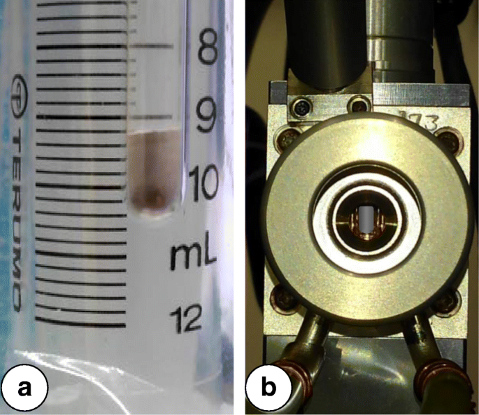
a의 DND 분말 사진 JEOL EPR 튜브 및 b X-밴드 마이크로파 공동의 중앙에 있습니다. 비교를 위해 EPR 튜브의 분말 이미지는 10 ml 부피의 플라스틱 주사기의 주요 부분에 대해 특별히 촬영되었습니다.
g가 있는 DND의 EPR 스펙트럼 -4.00–4.30 범위의 신호 요인은 마이크로파 전력, P로 기록되었습니다. MW =6 mW; 자기장 변조 진폭, A m =0.5mT; 주파수, ν =100 kHz; 이득, G =1200; 및 신호 축적, N =20. 시상수는 0.030 s였다. 하나의 자기장 스위프에 대한 기록 시간은 120 s였습니다.
스윕에 대한 최소 및 최대 자기장 값은 JEOL-JES 프로그램 소프트웨어로 특별히 선택되었으며 JEOL NMR Field Meter ES-FC5(Echo Electronics)로 정확하게 정의되었습니다. NV - 의 농도 센터는 해당 EPR 신호와 g의 이중 적분에 의해 추정되었습니다. =4.27, 해당 샘플 무게에 할당 및 참조 샘플의 EPR 신호 비교. 우리는 특별히 합성 형광성 Ib HPHT 다이아몬드 분말을 선택했습니다. 각주 3 (평균 크기 ~ 100 nm), g의 잘 정의된 통합 강도 =4.27 EPR 라인 및 알려진 농도 S =1 NV − 5.3 ± 0.4 ppm의 중심은 NV - 의 얻은 농도를 정확하게 결정할 수 있도록 하는 독립적이고 신뢰할 수 있는 참조입니다. DND에서. 이는 이전에 Shames et al.이 제안한 접근 방식과 유사합니다. [24]. 지 =4.27 EPR 라인은 다음 매개변수를 사용하여 이 참조 샘플에 대해 기록되었습니다. P MW =3 μW, A m =0.2mT, G =500, N EPR 라인의 피크 대 피크 강도가 샘플 공간에서 마이크로파 전력의 제곱근에 비례하는 선형 모드에서 =12. 서브미크론 및 미크론 크기 Ib HPHT 결정의 경우 이 체제는 일반적으로 낮은 마이크로파 전력(7–10 μW 미만)에서 잘 시행됩니다. 스펙트럼은 119~321mT의 광범위한 자기장에서 특별히 기록되었습니다. 이 범위는 Δm에서 추가 EPR 신호를 등록하기 위해 사용되었습니다. s =1 전환, 낮은 필드에서 허용되며 NV − 의 고유한 서명을 나타냅니다. 센터.
DND의 X선 광전자 분광법(XPS)은 단색 Al Kα 방사선 소스가 장착된 Perkin-Elmer PHI 5600 Multi-Technique 시스템을 사용하여 수행되었습니다. 광전자의 스펙트럼 특성은 ~ 1 mm 2 의 샘플 영역에서 방출되는 광전자 플럭스를 분석한 후 구했습니다. [25]. 감지된 광전자는 몇 개의 원자층 두께 영역(<2 nm)인 물질의 표면에서 방출됩니다. 탄소 C1, 질소 N1 및 산소 O1의 광방출 피크 영역 분석에 특히 주의를 기울였습니다. 광방출 피크를 개별 구성 요소로 분해하는 작업은 적절한 단일항 등고선 세트에 의해 수행되었습니다. DND 샘플의 스펙트럼은 아르곤 이온으로 표면을 에칭한 후 취했습니다. 이온 에칭은 3 kV의 가속 전압과 약 4 μA의 이온 빔 전류에서 3분 동안 수행되었습니다. Ar 이온 에칭은 샘플 표면에서 흡착된 주변 가스 및 기타 화학 흡착된 원자 복합체를 제거하는 데 사용되었습니다. XPS는 X선 CSR 크기가 다른 일련의 다양한 DND 샘플에서 내부 질소 함량을 평가하는 데도 사용되었습니다.
PL 연구를 위해 샘플은 4mm 구리판으로 만든 직경 2 mm의 얕은 구멍으로 분말을 밀어 넣은 다음 유리판으로 표면을 평평하게 하여 준비했습니다. PL 스펙트럼은 ~ 0.5 mW의 전력에서 532nm 레이저 여기와 밀리미터당 600개의 홈이 있는 회절 격자를 사용하여 맞춤형 마이크로 라만 설정을 통해 540–1000 nm 범위에서 기록되었습니다. 노출 시간은 180 s였다. 여기 방사선은 Nikon Plan Apo 100x, NA =1.40 현미경 대물렌즈를 통해 직경 2 μm의 지점으로 평평한 샘플 표면에 집중되었습니다. 스펙트럼 분해능은 0.05 nm보다 우수했습니다.
PL 스펙트럼을 등록하고 커버 유리에 스핀 코팅된 DND 입자의 PL 신호를 매핑하기 위해 추가 PL 설정을 사용했습니다. 이미징 분광기와 결합된 맞춤형 도립 공초점 주사 현미경으로 구성되어 있습니다. 공초점 현미경은 압전 주사대(NanoPDQ75, Mad City Labs Inc., USA), 현미경 대물렌즈(Plan Apo 100×, NA =1.40, Nikon, Japan) 및 광학적으로 펌핑된 반도체 레이저(Verdi, Coherent Inc., 미국) 이색성 빔 스플리터(z532rdc, Semrock, USA)를 통해 대물렌즈에 주입되는 532 nm의 파장에서 방출합니다(원형 편광, 0.5 mW 전력). 검출 경로는 공초점 제거를 위한 50μm 직경의 핀홀, 대역통과 필터(FF01-697/75, Semrock) 및 단일 광자 계수 모듈 검출기(SPCM-AQR-14, Perkin-Elmer, Canada)로 구성됩니다. . 이미징 분광기는 후면 조명 CCD 어레이 검출기(DU440-BU2, Andor Technologies, UK)에서 스펙트럼을 이미징하는 오목 격자로 구성되어 약 1 nm의 스펙트럼 분해능을 제공합니다.
발광 신호의 매핑은 20 × 20 μm 2 에 걸쳐 수행되었습니다. 정사각형. 측면 방향의 기본 스테이지 변위는 정확도 ~ 1 nm에서 100 nm였습니다. 500–900 nm 범위의 PL 스펙트럼과 해당 스펙트럼의 최대값에서 PL 강도의 시간 의존성을 얻기 위해 기판에서 발견되는 측면 크기가 0.6 마이크론 이하이고 강한 발광성을 갖는 여러 DND 집합체 중 2개를 선택했습니다. . 노출 시간은 등록된 각 2D PL 맵에서 각 PL 스펙트럼에 대해 60 s, 픽셀당 3 ms였습니다. 회절 제한 스폿 크기(점 확산 기능, PSF)는 약 2-3픽셀(250 nm)을 커버합니다. 커버 유리 기판의 약 1mm 이내로 가져온 영구 자석을 사용하여 자기장을 가했습니다. 샘플 위치의 자기장 강도는 약 ~ 90–100mT였습니다. PL 신호의 시간 의존성은 샘플이 있는 표면에 자석을 빠르게 접근하고 제거하는 과정을 반복하여 기록되었습니다.
컬러 센터에서 방출되는 방사선은 sp에 의해 흡수될 수 있기 때문에 2 - DND 내부에 존재하는 함유 종은 입자 사이 공간의 특정 형태적 특징에 의해 차단될 수도 있으며 NV를 제어하고 모니터링하는 것이 매우 중요합니다. - 비 광학적 방법으로 다이아몬드의 중심. NV − 중심은 EPR 분광법으로 여기 및 발광 광학 복사를 모두 차단하는 불투명하고 조밀한 매체에 캐리어를 삽입하거나 NV - 가 없는 경우에도 감지할 수 있습니다. 특정 담금질 메커니즘과 관련된 2차 방사선. 이들의 총 농도는 이후에 EPR 스펙트럼의 분석에 의해 쉽게 평가될 수 있습니다[16, 26, 27]. 동시에, NV - 의 결정된 농도 센터는 NV − 의 잠재적(광범위한 정화 후) 밝기에 대한 귀중한 정보를 제공합니다. PL. 소위 반자계 영역에서 3차원 전이금속 자성 불순물(대부분 Fe, Ni)로부터 정제된 DND 분말의 EPR 스펙트럼은 그림 2(검은색 곡선)에 나와 있습니다. 스펙트럼은 g가 있는 두 개의 가까운 선(1 및 2)으로 구성됩니다. -요소 g 1 =4.27 및 g 2 =4.00, 너비 ΔH pp1 ≈ 2.0mT 및 ΔH pp2 ≈ 1.4mT. 첫 번째 낮은 필드 라인은 금지된 전환 Δm에 해당합니다. s =2 NV의 삼중항 상태의 Zeeman 에너지 준위 − 자기장의 중심. 두 번째 하이필드 라인은 동일한 금지된 전환 Δm에 해당합니다. s =2, 마이크로파 복사가 다른 중심, 즉 S를 갖는 다중 공석에 의해 흡수될 때 발생 =1. Ref. [16], 이 계통은 먼저 DND에 공존하는 서로 다른 삼중항 중심에 할당되었으며, 특히 g 1 =4.27 라인이 NV − 에 할당되었습니다. 센터. g의 위치 1 =4.27 선은 금지된 전이 Δm의 선에 해당합니다. s =2 일중항-삼중항 NV − 의 기저상태 에너지 다이어그램에 나타난 바와 같이 최대 300mT의 자기장 중심(그림 3). 스핀-해밀토니안(D =850 × 10 −4 cm −1 ), 삼중항 NV - 에서 구성 스핀의 강한 교환 상호작용으로 인해 발생 중심, g 위치의 높은 감도를 유발합니다. 1 =4.27 라인(g에서 0.5% 이동) -스케일) 9.0 ~ 9.9 GHz(X-밴드) 범위의 특정 마이크로파 주파수 [26]. 라인 g의 적분 강도 1 =4.27은 NV − 의 농도를 정확하게 추정하는 데 사용할 수 있습니다. 나노다이아몬드의 발광이 인접한 광학 활성 종으로 인한 흡수 또는 소광으로 인해 감지할 수 없거나 세 번째 공존 종으로부터의 강한 기생 배경 발광에 의한 차폐로 인해 중심에 위치합니다. NV - 의 농도가 알려진 고에너지 전자 조사, 합성, 서브마이크론 다이아몬드(평균 크기 100 nm) 센터는 참조 샘플(샘플 Ib HPHT FND)로 사용되었습니다. 낮은 마이크로파 전력 P에서 취한 샘플 Ib HPHT FND의 EPR 스펙트럼 MW =3 μW는 비교를 위해 그림 2(빨간색 곡선)에 표시됩니다. 320mT 미만의 범위에서는 "금지된" Δm에 해당하는 3개의 잘 정의된 EPR 신호로 구성됩니다. s =2(157.85mT에서) 및 2개 허용 z , Δm s =1 및 x ,y , Δm s =1(234.39mT 및 281.27mT에서) NV − 의 지상 삼중항 상태의 Zeeman 에너지 준위 간 전환 자기장에서. Δm s =2 및 z , Δm s =1 전이는 그림 3의 구성표에도 표시됩니다. NV - 가 있는 서브미크론 기준 샘플과 비교할 때 상당히 놀라운 중앙에서 DND 입자는 g =4.27 Δm과 관련된 EPR 라인 s =2 "금지된" 전환. 특히 허용되는 z , Δm s =1 및 x ,y , Δm s =1 마이크로파 전이는 관찰되지 않습니다. 가능한 설명은 Δm와 관련된 EPR 라인의 비정상적인 확장입니다. s =1 스핀-해밀턴의 주요 매개변수의 큰 변동으로 인한 전환(D 및 E ) S =1 NV − DND 입자의 앙상블을 통해. 따라서 허용된 z와 관련된 줄이 완전히 없습니다. , Δm s =1 및 x,y, Δm s =1 전환은 NV − 의 독특한 핵심 기능입니다. DND에서. 상업용 공급업체에 따르면 NV − 의 예상 농도는 흡수 조사선량을 기준으로 평가된 참조 Ib HPHT에서 FND는 ~ 5.3 ppm이었습니다. g의 적분 강도 1 =4.27 DNDs' EPR 스펙트럼의 라인은 Ib HPHT FND EPR 스펙트럼보다 ~ 4.8배 더 작은 것으로 밝혀졌고, 따라서 NV - 의 농도 DND의 중심은 1.1 ± 0.3 ppm으로 결정됩니다. 배경 보정과 함께 반 자기장 범위(130–180mT)의 두 EPR 신호 통합에 대한 해당 절차는 특별히 그림 4에 나와 있습니다. 그림 4a에는 1차 도함수의 원래 측정된 EPR 스펙트럼이 포함되어 있습니다. 수학적 처리 이전의 마이크로파 흡수(곡선 1); 적분 후 동일한 EPR 스펙트럼(상단 곡선 2); 및 측정된 원래 EPR 스펙트럼과 동일하지만 나머지 철 함유 착물과 관련된 넓은 로렌츠 유형 선을 뺀 후(하단 곡선 3). 그림 4b는 배경 보정된 측정된 EPR 스펙트럼을 통합한 후 참조 샘플(상단 곡선)과 DND(하단 곡선) 모두의 EPR 스펙트럼을 보여줍니다. DND 자체에 대한 진정한 통합 스펙트럼(그림 4b, 하단 곡선)은 수정되지 않은 DND의 측정된 EPR 스펙트럼만 통합된 그림 4a의 두 번째 스펙트럼과 상당히 다릅니다. 얻은 스펙트럼(그림 4b, 하단 곡선)은 인접 EPR 신호(g 1 =4.00 및 g 2 =4.27) ~ 10mT 거리로 분리된 Lorentz 유형. 그림 4의 패널(b)에 표시된 EPR 스펙트럼 아래 음영 영역은 선 g의 적분 강도를 나타냅니다. 1 두 비교 샘플에 대해 =4.27. 샘플 가중치로 정규화했을 때 이러한 영역의 비율은 약 ~ 4.8입니다. 흥미롭게도 DND의 경우 g 1 =4.27은 대칭적이고 넓습니다. 이 라인은 부분적으로 상위 필드 g와 중첩됩니다. 2 =4.00 다중 공석으로 인한 EPR 라인. 강한 기준선의 형태로 남아 있는 보정되지 않은 배경(주로 제거할 수 없는 철 관련 복합체에서)은 그림 4a(스펙트럼 2)에서 명확하게 볼 수 있습니다. 따라서 130–180mT 범위에서 최소 3개의 중첩된 구성요소에 대한 DND의 EPR 스펙트럼의 정확한 분해는 g =4.27 NV − 의 선과 농도 . 우리는 또한 500 °C 미만의 온도(진공 및 공기 중)에서의 다양한 처리가 NV - 농도에 실질적인 영향을 미치지 않는다는 것을 발견했습니다. DND의 센터. 신호 g의 이중 적분 강도 1 =4.27(ν의 경우 ~ 151mT에 중심을 둔 Lorentzian 등고선 아래의 그림자 영역 =9.0785 GHz)는 처리 후에도 이전과 거의 동일하게 유지됩니다. 이것은 NV - 중심은 적어도 격자 상수(~ 0.36 nm)의 나노 입자 표면 깊이에서 격자에 충분히 깊게 묻혀 있으므로 다이아몬드 상을 에칭하거나 침투하지 않는 외부 화학 작용제와 반응할 수 없습니다.
<그림>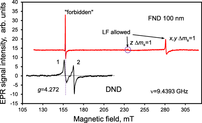
반자계(검은색 곡선) 영역에서 산 정제된 DND의 EPR 스펙트럼과 최대 320mT 범위에서 평균 크기가 ~100 nm(빨간색 곡선)인 기준 전자 조사 형광 Ib HPHT 다이아몬드 나노입자. DND EPR 스펙트럼의 두 라인은 숫자 1과 2로 표시됩니다. g가 있는 로우 필드 라인 1 =4.272는 NV − 에 해당합니다. 센터. 로우필드(LF) 관련 라인 허용 z Δm s =1 및 x ,y Δm s =1 FND 100 nm의 전이는 위쪽 스펙트럼에 대한 화살표로 표시됩니다. 허용된 z와 관련된 가장 약하고 거의 구별할 수 없는 줄 Δm s = 1 transition is additionally marked by a circle. The microwave frequency was 9.4393 GHz

Energy diagram of ground singlet-triplet levels 3 A2 of NV − in magnetic field up to 300 mT. “Forbidden” Δm s = 2 and LF allowed Δm s = 1 transitions caused by absorption of microwave radiation (ν ≈ 9.44 GHz) are marked by vertical red arrows. The position of the ground state spin level anti-crossing (|0 〉GS and |−1〉GS ) is marked by a circle

아 Background subtraction in EPR signal of DND and b estimations of the double-integrated intensities of the g = 4.27 line for a DND sample and reference fluorescent Ib HPHT synthetic diamond. 패널 a :as-registered first derivative EPR signal of the DND in the ± 15 mT half magnetic field range (curve 1, blue); the same, but integrated EPR signal in the same ± 15 mT range of magnetic field (curve 2); the same first derivative EPR signal of DND, but after subtraction of the broad parasitic EPR signal from remaining non-removable iron-containing paramagnetic complexes shown by red contour of Lorentzian shape in the upper curve (curve 3, blue). 패널 b :Estimation of the double integrated intensity of the g = 4.27 line for a fluorescent Ib HPHT diamond having NV − (upper curve, shaded area) and the DND sample (bottom curve, shadow area). The bottom spectrum in panel b consists of two contours of Lorentzian shape, one of which centred at lower magnetic field (≈ 150.932 mT), is assigned to the NV − centres of DND (the area below this contour in red is highlighted). Microwave frequency:ν = 9.0785 GHz
The main high-intensity EPR signal of the DND lies above 320 mT at ν = 9.4393 GHz and has a g -factor g ≈ 2.0027. It has a Lorentzian curve profile of linewidth ΔH pp = 0.84 mT [13]. This linewidth is greater than that of fluorescent nanodiamonds (FNDs, 100 nm) milled from microcrystalline diamond synthesized by a high-pressure and high-temperature method. The broad signal can be explained by greater exchange and dipole-dipole interactions between the S = 1/2 spins in the spin ensemble within an individual DND nanoparticle than those within a FND. The intensity of the main EPR signal collected from all S = 1/2 paramagnetic centres, both of nitrogen (P1 centres [28]) and non-nitrogen origin, indicates a spin concentration of ~ 1300 ppm, corresponding Footnote 4 to around 15 S = 1/2 spins in each DND [13]. However, it can be concluded from the earlier obtained data that approximately 40–50% of the total number of all paramagnetic centres in the DNDs are due to half-populated antibonding orbitals of isolated P1 centres. Thus, the huge total of spin-half, point-like agents located in DNDs (N PC ) can be represented as the sum of at least two contributions, from P1 centres and from elemental point defects having dangling bond spins ½, for example based on vacancies like H1 centres (VH o ):\( \left({N}_{\mathrm{PC}}=\left[{\mathrm{N}}_{\mathrm{s}}^{\mathrm{o}}\right]+\left[\mathrm{et}\ \mathrm{al}\ \right]\ \right) \). Here we assume that specific EPR signatures from the hyperfine structures of P1 and H1 centres are absent or greatly “smeared” through the dense arrangement of localized spins within each particle. This sum gives us a clue about the approximate content of both isolated nitrogen and monovacancies inside the DND, although isolated nitrogen and monovacancies can also be present in the diamond lattice in nonparamagnetic forms such as \( {\mathrm{N}}_{\mathrm{s}}^{-},{\mathrm{N}}_{\mathrm{s}}^{+} \), V o . The presence of H1 centres together with neutral monovacancies in DND at some minor level (< 700 ppm) is reasonable in principle because rapid assembling of diamond lattice during the detonation takes place from hydrogen-containing products of TNT-hexogen pyrolysis such as CH3 * or CH2 * radicals. Although the mutual charge transfers between the main groups of centres present in the lattice in various charge and spin states (\( {\mathrm{N}}_{\mathrm{s}}^{\mathrm{o}},{\mathrm{N}}_{\mathrm{s}}^{-},{\mathrm{N}}_{\mathrm{s}}^{+};{\mathrm{V}}^{-},{\mathrm{V}}^{\mathrm{o}} \)) are possible in principle, the foremost contribution to paramagnetism comes from only \( {\mathrm{N}}_{\mathrm{s}}^{\mathrm{o}} \). Let us therefore estimate the maximal possible concentration of NV in a DND on the basis of assumptions about the known total amounts of substitutional nitrogen and monovacancies inside the particles. The actual charge state of NV is not essential for such an estimation. A statistical approach gives the following simple formula for the probability (p NV ) of finding at least one NV in one 5-nm DND particle consisting of N nodes of covalent diamond lattice:\( {p}_{\mathrm{NV}}=\frac{2 nv}{N} \) , where n 및 v are the mean numbers of isolated nitrogen atoms and monovacancies inside the DND particle, respectively. Because N PC ≈ 1300 ppm, we can approximately assume that n + v ~ 15 for N = 11,500. The maximal value of p NV is achieved when \( n\approx v\approx \frac{15}{2} \). This gives p NV ≈ 0.0098. This value corresponds to around ~ 1 ppm of NV in DND, as was obtained previously from comparison of the g = 4.27 EPR signals of the DND and the reference sample. Excluding the surface nodes linked with surface functional groups and interior nodes occupied by A-centres (up to 2 at.%) from the formal integration procedure, using N = 9950–10,000 gives a slightly greater concentration of NV, up to 1.1 ppm. The estimated experimental concentration of NV − centres in the DNDs is in close agreement with the theoretical estimation made above, and about 1000 times smaller than the concentration of all S = 1/2 paramagnetic species in the system.
The concentration ratio for interior S = 1/2\( {\mathrm{N}}_{\mathrm{s}}^{\mathrm{o}} \) and S = 1 NV − centres is therefore qualitatively consistent with the main idea of rapid NV centre formation, that is, from the “random inclusion” of both substitutional nitrogen atoms and vacancies to the growing diamond nano-crystallites during the overall ~ 13–20 μs duration of the detonation wave propagation. Here, we intuitively assume that each NV − is formed as a result of the random embedding and occurrence of impurity nitrogen atoms and vacancies in the nearest neighbour lattice sites during the period of time prior to the subsequent rapid cooling of the products to temperatures of the order of ~ 500–650 °C at which the diffusion of vacancies in the lattice is practically stopped.
XPS is a powerful tool for studying the DNDs’ composition and the chemical state of the main alien elements present on the surface of the DNDs (and also within 2 nm under the surface) [29]. Our main interest was focused on the XPS signal from nitrogen and the evaluation of the interior nitrogen content, since nitrogen is the predominant inner impurity. The XPS signals of carbon (C1s), nitrogen (N1s) and other elements have been recorded after etching of the surface with Ar ions. An overview of the XPS spectrum plotted in the wide range of binding energies from 250 to 600 eV is shown in Fig. 5a. Although the data indicates the presence of a large amount of oxygen-containing atomic groups at the DND’s surface (5.5 at.%), the analysis of the O1s signal is not of particular relevance to this work. The concentration of both inner and exterior nitrogen was preliminarily evaluated to be between 1.7 and 2.4 at.% [30]. The concentration of all the residual elements found (a small number of metals) did not exceed ~ 0.32 at.% in the as-received DND, and it could be reduced by 20–30 times by etching the DND powder in boiling aqua regia and hydrochloric acid [30]. The photoemission peak of nitrogen (N1s) is shown in Fig. 5b. Etching with Ar ions results in the removal of weakly bound adsorbed species from the surface, while the covalent diamond lattice remains unaffected. The characteristic high-energy peaks (~ 404.6 eV and 407.3 eV) in the N1s photoemission signal have very low intensities when compared with an untreated pristine sample. These peaks demonstrate the presence of any remaining nitrate ions (peak at ~ 407.3 eV) and nitrite groups (peak at ~ 404.6 eV) on the Ar ion-treated surface. Further complete removal of nitrate ions and nitrite groups from the surface can be achieved only by annealing the DND powder in air at temperature> 350 o C. The main peak of the N1s signal at ~ 401 eV, which is not influenced by Ar ion treatment, corresponds to chemical bonds of the type N–sp 3 –C. This peak is a characteristic of interior elemental nitrogen covalently bound within the diamond lattice. It appears due to various forms of nitrogen present in the diamond matrix, including NN dimers, next nearest neighbouring N + ...N − pairs, and more complex nitrogen clusters. Similar data were obtained for the photoemission peak of carbon C1s (sharp, intense signal seen in Fig. 5a, see also Ref. [30] for details). The C1s XPS signal consists of two main peaks:one centred at 284.9 eV corresponding to C–C bonds in the diamond matrix and another peak centred at 287.3 eV corresponding to C–N bonds. Only diamond carbon and sp 3 /sp 2 carbon bound to nitrogen, even in the form of atomic-scale disordered nitride phase species (where neighbouring carbon and nitrogen atoms can have up to three C–N bonds), are represented in the C1s signal of the Ar ion-treated surface. Our careful analysis of the integrated intensity of only the N1s 400.9 eV peak and C1s signals (together with O1s and residual elements’ signals) suggests that nitrogen is contained within the diamond lattice of selected DND sample in the amount of 1.65 ± 0.05 at.% and mainly in the form of complex clusters which are not paramagnetic. This value was obtained after special correction by a reducing factor taking into account that the actual size of DND particles is larger than the whole depth of crystal lattice from which the excited photoelectrons are readily emitted. It seems that only a small part of nitrogen is present in the diamond lattice in the form of isolated paramagnetic nitrogen atoms with spin S = 1/2 (no more than 8–9% of all nitrogen). The isolated paramagnetic nitrogen atoms are only accessible for observation by EPR as was shown in the previous section.

XPS spectra of acid-purified DNDs after Ar ion etching:a overview of the spectrum in the range 250-600 eV and b N1s photoemission peaks
XPS spectroscopy was also applied to estimate the nitrogen content in other DND samples provided by our suppliers. We found that the nitrogen content varies in these samples from ~ 1.6 at.% (minimal value) to ~ 2.1 at.% (maximal value). We simultaneously noticed that higher concentrations of nitrogen correspond to the samples with a smaller X-ray CSR size. Such values of nitrogen content were also roughly confirmed by elemental analysis with a Micro Corder JMC10 device in the course of sample combustion in oxygen flow (30 ml/min) at 1000 o C. As a reference source of nitrogen, carbon and hydrogen for this method, we used the antipyrine C11 H12 N2 O, having nitrogen in its structure in the form of N–N groups.
The PL spectrum of one selected powder DND sample is shown in Fig. 6a. It has the maximum intensity at 680 nm. Following [31], a characteristic spectrum with peak position above 650 nm indicates the presence of both NV − and NV 0 defects, although the contribution from some light-emitting defective sites of remaining sp 2 -coordinated carbon species around DND particles cannot be excluded completely. However, the characteristic zero-phonon lines (ZPL) at 638 nm (NV − ) and 575 nm (NV 0 ), respectively, are not detected. This probably occurs due to the changing positions of the NV 0 and NV − excited/ground states inside the bandgap for centres lying in the vicinity of the particle edge and the subsequent broadening of the 638-nm and 575-nm ZPL spectral components for the ensembles of such NV 0 and NV − centres with slightly different electronic parameters. Let us mark that the absence of featured NV − ZPL peak at 638 nm was confirmed in many studies related with photoluminescence of DND aggregates lying free on the substrate or embedded inside polymers [31]. Sometimes it (suppressed or very poorly recognized ZPL feature at 638 nm) even happens for larger isolated fluorescent Ib HPHT nanodiamonds of a size about 40 nm [4].

아 Photoluminescence spectrum of DND powder pressed flush in a shallow hole with a diameter of 2 mm made in a copper plate and b the interior nitrogen content measured by XPS and c the intensity of NV − PL at 680 nm as a function of X-ray CSR size for a series of selected DNDs synthesized in the presence of some intentionally added inorganic additives in the detonation zone (charge and water shell) as provided by the manufacturer. Excitation laser wavelength λ = 532 nm, power ~ 0.5 mW. The diameter of the focused laser spot on the sample surface was 2 μm. Conditions of recording were temperature T = 293 K, and an air environment
We also studied the PL intensity for a series of DND samples with different CSR sizes. The CSR size characterizes the average size of perfect diamond domains or the mean size of diamond nano-crystallites in the powder even if they are randomly arranged in large-scale polycrystalline aggregates with size exceeding 30–50 nm. The CSR size varied from 4.3 to 5.6 nm in the series of DND samples selected for our studies (similar to the results explained in Ref. [32] although we used another more traditional approach for analysing X-ray diffractograms). Figure 6b shows the dependence of interior nitrogen content evaluated by means of the XPS method versus the CSR size of the DNDs. The larger the CSR size, the smaller the nitrogen content. This seems reasonable as powders with larger DND particles were synthesized as a result of the addition of some inorganic substances having the elements playing the role of nitrogen-getter inside the detonation zone (charge or charge enclosure). Such elementary additives probably promote the reduction of the overall nitrogen content in the growing diamond lattice during the explosion process or change the conditions of the diamond lattice assembly to slightly prolong the synthesis (on the order of microseconds). In addition to the overall nitrogen content, we also recorded the reduced amount of nitrogen-related paramagnetic centres in these DNDs, as confirmed by EPR spectroscopy. PL spectra of all DNDs having different CSR sizes are practically the same in shape in the range 550–900 nm, but this is not the case for the absolute intensities of the PL at the maxima of the PL spectra at 650–680 nm. The intensity at the maximum of PL spectrum is plotted in Fig. 6c as a function of the X-ray CSR size of the DNDs. Comparing both panels (Fig. 6b, c) it is clearly seen that the smaller the nitrogen content in DND, the higher the NV − PL intensity. Again, this seems reasonable as nitrogen-related centres and especially A-centres can act as effective quenchers of PL if the NV − light-emitting centres in some DND particles (one per a hundred of 5 nm DND particles at least) are surrounded by a “gas” of A-centres and other lattice imperfections, similar to the approach proposed in Ref. [33]. This trend gives us a hint at possible ways to enhance the intensity of luminescence from ensembles of DND particles by manipulating their size and nitrogen concentration. Among them, there is the technological enlargement of the mean size of DND particles in the course of their treatment at high pressure and high temperature at appropriate conditions, promoting their recrystallization and further crystal growth [34]. The probable reduction of NV − content through treatment leading to the reduction of A-centres and other interior defects in the diamond lattice may be compensated in principle by the opposite trend, promoting the brightness of NV − emission, and reducing the amount of all types of PL quenchers in the system, and hence, substantially improving the crystal quality of particles with sizes exceeding a dozen nanometres [34, 35]. Further works on these topics are now in progress.
Characterizing the fluorescence from isolated DND particles or submicron aggregates is crucial both for understanding their potential use as fluorescent markers and to help to mitigate disadvantages related with a relatively low concentration of NV − in them as determined by EPR. Photoluminescence was recorded for DND aggregates spin-coated on a glass microscope coverslip from an aqueous suspension with an average size of DND aggregates about 30 nm (as measured by dynamic light scattering).
Figure 7a shows two PL 2D maps obtained by confocal microscopy, using a 532-nm wavelength excitation laser with 100-μW output optical power. Bright spots corresponding to DND aggregates up to 500–700 nm in lateral size are observed. Dimmer spots of size around the optical diffraction limit are also observed after selection of the appropriate isolated spots. Figure 7c shows the intensity distribution along the specially selected straight line aa plotted in Fig. 7a. This line crosses about six dim spots of smallest diameter—five spots (1–5) are crossed by the straight line fairly precisely along their centres and one spot (6) is with a small displacement from this line. The corresponding five peaks in intensity distribution are clearly seen in Fig. 7c. Thus, each dim spot 1–5 laying on the line aa corresponds to the DND aggregate of smallest lateral size (in the range below 70 nm). It is possible that all of them are fixed on one V-shaped straight groove existing on the glass coverslip. We successfully fitted each peak in the intensity distribution with a 2D Gaussian \( {A}_i{e}^{-\left[{\left(x-{x}_{oi}\right)}^2+{\left(y-{y}_{oi}\right)}^2\right]/2{s}_i^2} \), where x oi , y oi are the Cartesian coordinates of the centres of the dim round spots, A 나 -maximum PL intensity of each isolated spot, s 나 is a parameter close to s 오 ≈ r 오 /3, where s 오 is a 1/3 part of the Airy disk diameter r 오 . In our case, for λ = 532 nm radiation (in vacuum) and numerical aperture of microscopic objective NA = 1.40, we have the following values for r 오 그리고 s 오 :r 오 =1.22λ/2NA ≈ 232 nm and s 오 ≈ 77 nm. The s 오 value in the 2D Gaussian determines the point spread function (PSF) of and ideal point-like emitter, i.e. the diffraction limitation related with the smallest possible interference ring. For the five peaks mentioned above (i = 1–5) we found the following s 나 values, respectively:85, 77, 77, 84 and 77 nm. Peak 5 has both the highest intensity and s -value equal to the theoretical value s 오 ≈ 77 nm. This means that the lateral size of the corresponding emitter for peak 5 is significantly smaller than the PSF size. The same is also true for peaks 1–4. We can conclude that the lateral sizes of DND aggregates laying along line aa are in the range below 70 nm. Each spherically shaped DND aggregate of ~ 30 nm in size Footnote 5 consisting of individual 5-nm particles (percentage of voids is 50%) has about 1.3 NV − centres in accordance with the 1.1 ppm content of NV − determined previously. This value is great enough in principle to distinguish aggregates of this size by optical methods. Each of the five aggregates lying along the line aa probably has between 2 and 10 colour centres. The larger the height of the DND aggregate lying on the substrate, the higher the density of luminescence centres (per unit square) for the light emitted more or less perpendicular to the surface. For aggregates with height up to 300–350 nm, the brightness of PL intensity can be at least one order of magnitude greater than that for aggregates of smaller 25–30 nm size. The PL spectrum of one selected aggregate of high brightness (marked by a circle in the 2D map presented in Fig. 7a) was studied in detail. It has roughly the same shape (especially on the right wing above 680 nm) as that for the spectrum shown in Fig. 6a and indicates the presence of both NV − and NV 0 결함. However, the characteristic zero-phonon lines (ZPL) at 638 nm (NV − ) and 575 nm (NV 0 ), respectively, were again not detected. ZPLs are usually well resolved only for diamond crystals of micron size or larger, while for nanometre-scale crystals, they are typically not well-observed due to some experimental or other physical reasons Footnote 6 . Let us mark that for DND aggregates lying on the cover glass, the final treatment with UV/O-Cleaner removed the sp 2 -coordinated carbon species around the particles inside the aggregates and as a result the PL spectrum is free from the contribution of light-emitting centres of disorganized sp 2 -carbon phase.

아 2D-colour mapping of the PL signal intensity of DND spin-coated on a glass microscope coverslip together with b schematics of the experimental setup. ㄷ The PL intensity profile along the “aa” cross-section. d The photoluminescence intensity versus time for the selected DND aggregate marked with a circle in the upper side of the 2D map shown in panel a , in the presence or absence of an external magnetic field. Laser excitation at 532 nm wavelength. Square, 201 × 201 pixels. Integration time is 3 ms/pixel. Step—100 nm. The excitation radiation is focused on the upper surface of the glass coverslip with deposited DND. In zero field (B = 0), only small changes of intensity, due to the blinking of some of the NV − colour centres occur. When magnetic field is temporally applied a large decrease of the PL intensity occurs. Upper left panel a :the left scale for PL intensity corresponds to the 2D mapping of another DND aggregate shown in the left bottom corner of the large 2D map. Upper right panel b :schematics of the experimental setup explaining the displacement of the permanent magnet above the coverslip relative to the deposited DND
To confirm the presence of NV − centres in the DND, we studied the influence of an external magnetic field on the PL intensity. No PL modification is expected from NV 0 , which have no magneto-optical properties unlike NV − . Figure 7d shows the meander-like time variation of the PL intensity from an isolated DND aggregate in the presence of an external magnetic field switched “ON” by quickly bringing a compact permanent magnet close to the DND or by removing it (“OFF”). This occurs as a result of the mixing of the |0〉GS and |−1〉GS states of NV − centres at the ground-state spin level anti-crossing (GSLAC), marked with a circle at magnetic field ~ 100 mT in Fig. 3. Such mixing leads to a change in the populations of these states, accompanied by a PL intensity decrease. The optical transitions between the ground 3 A2 and excited 2 E triplet states preserve the spin quantum number (Δm S = 0). However, from the m S = ± 1 excited state, the optical excitation of NV – also decays with no radiation in the visible domain, through a system of two metastable singlet states before coming back to the ground state [5]. This process is accompanied by radiation at a longer wavelength of 1042 nm defined by the gap between these two singlet levels with S = 0. This additional decay pathway results in a lower fluorescence intensity from the main radiation transition within the m S = ± 1 subsystem of ground and excited triplet states. The experimentally detected decrease of NV – centre PL intensity is quite reasonable in the presence of a weak (≤ 100 mT) magnetic field [36], as observed in Fig. 7d. Surprisingly, in our case (for DNDs), this drop is essentially larger than those reported in the literature for Ib HPHT fluorescent microdiamonds and even evaluated theoretically in the framework of the standard NV model [37].
In this article, we have shown that nitrogen-vacancy centres appeared in the interior of 5 nm nanodiamond particles synthesized by detonation of nitrogen-containing explosives are the main triplet colour centres. Precise counting of the number of NV − centres was achieved. The DNDs contain ~ 1.1 ppm of such NV − centres in the crystalline diamond lattice. This value is just five times smaller than that detected in the bright fluorescent reference Ib HPHT diamonds with a mean size of about ~ 100 nm. Our adjusted and rechecked estimation made on the basis of the EPR method is about three orders of magnitude larger than that evaluated in Ref. [38] by pure optical methods for DND aggregates. Probably not all NV − centres detected by EPR are optically active due to the NV − luminescence quenching by various point and collective defects located near the surface. Annealing DNDs in oxygen- or ozone-containing air removes defects associated with light-absorbing sp 2 carbon at the particle surface and allows detection of the specific PL of NV − centres. When an external magnetic field is applied, an accompanying variation of the PL intensity is observed. This is the result of the sensitivity of the NV − triplet ground state to magnetic field and comes through the mixing of the |0〉GS and |−1〉GS states of only the NV − centres below/near the GSLAC point leading to the decay of the optical excitation with no radiation in the visible domain. The application of this effect to discriminate ultra-small DND emitters in an environment with a large autofluorescence background and micron-scale bio-object contouring is promising [39]. Some DND aggregates playing the role of point-like NV − emitters and giving the smallest fluorescent spots with diameter close to the PSF size (diffraction limitation) were found.
The same data for concentration of paramagnetic centres S = ½ (≥ 1260 ppm) were obtained independently by precision measurements of the magnetization field dependence at temperature T = 2 K using a superconducting SQUID magnetometer. The magnetization curve does not show the presence of spins 3/2 in appreciable quantity in DNDs [13].
See for example the details of this method for analysis of the standard (DND) and non-standard (NDB-G) samples given in Ref. [22].
Fluorescent Ib HPHT (high pressure high temperature) microcrystals doped with nitrogen (100–150 ppm) and thereafter irradiated by high energy electrons (2–15 MeV) and annealed at 800–950 o 다.
We assume that a typical DND particle (with size slightly exceeding 5 nm) consists of ~ 1.1 × 10 4 carbon atoms.
Here we consider the typical DND aggregate in water DND suspension used for deposition the aggregates on the glass coverslip. Certainly, the actual shape of aggregates lying on the cover slip can be rougher and extremely diverse depending upon the adhesion of DND particles to the glass and actual size of the large-scale aggregates.
The ZPL line at 638 nm was not resolved in many works where the nanodiamonds having NV − were studied [4, 31]. It is probable that the various local environments of NV − centres in nanosized diamond (like surface defects and interior imperfections) greatly disturb the position of NV − triplet ground states in the bandgap.
2차원
충전 결합 장치
Detonation nanodiamond
Electron paramagnetic resonance
Fluorescent nanodiamond
Ground state spin levels anti-crossing
High pressure high temperature
조리개 수치
Nitrogen-vacancy
Optically detectable magnetic resonance
광발광
Point spread function
Special design and technology bureau
초전도 양자 간섭 소자
자외선
X선 광전자 분광법
X선 회절
Zero-phonon line
나노물질
초록 우리는 솔루션에서 보호되지 않은 GaN 나노와이어의 광발광(PL) 응답을 보고합니다. 뚜렷한 반응은 pH뿐만 아니라 동일한 pH에서 이온 농도에 대한 것입니다. 나노와이어는 높은 이온 농도와 1까지의 낮은 pH 값을 갖는 수용액에서 매우 안정한 것으로 보입니다. 우리는 PL이 다양한 유형의 산성 및 염 용액과 가역적 상호작용을 갖는다는 것을 보여줍니다. 나노와이어의 양자 상태는 외부 환경에 노출되어 산의 음이온에 의존하는 직접적인 물리적 상호작용을 갖는다. 이온 농도가 증가함에 따라 화학 종에 따라 PL 강도가 증가하거나 감
초록 소개 다이아몬드의 질소-결손(\({\text{NV}}}^{ - }\)) 중심은 치환된 질소와 인접한 공석으로 구성되어 여러 과학 기술 분야에서 폭넓은 관심을 불러일으켰습니다. 미래 양자 컴퓨터의 양자 메모리[1], 매우 민감한 자력계[2] 살아있는 세포[3] 및 뉴런 활동의 생체의학 이미징에 응용되고[4], 다양한 초해상도 이미징 방법에서 원자 규모 프로브로 사용 STED(Stimulated Emission Depletion) 현미경과 그 스핀 변형, GSD(Ground-State Depletion) 현미경의 변형[5,