높은 자외선 검출 효율을 위한 4H-SiC 분리된 흡수 전하 및 곱셈 Avalanche 포토다이오드 구조의 최적화 전략
초록
이 작업에서 구조 최적화에 대한 매개변수 조사는 4H-SiC 기반 분리 흡수 전하 및 곱셈(SACM) 애벌랜치 자외선 광다이오드(UV APD)에 대해 체계적으로 이루어집니다. 우리의 결과에 따르면, 항복 전압은 곱셈층의 두께와 전하 제어층의 도핑 농도에 의해 크게 영향을 받을 수 있습니다. n형 오믹접촉층, 흡수층, 전하조절층의 두께는 광투과 깊이에 현저한 영향을 미칠 수 있으며, 이는 광 발생 전자-정공 쌍의 수에 상응하는 영향을 미치므로 앞서 언급한 층 두께는 SACM APD의 반응성에 강한 영향을 미칩니다. APD의 응답성을 향상시키기 위해 우리는 광흡수층과 전하 제어층의 계면에서 감소된 에너지 밴드 장벽 높이를 필요로 하며, 이로써 증배층으로 촉진된 캐리어 수송이 유리할 수 있다. 또한 메사 가장자리에서 전기장을 줄이기 위해 더 작은 각도로 양의 경사 메사를 조사합니다. 따라서 암전류가 그에 따라 억제됩니다.
소개
와이드 밴드갭 반도체 재료로서 탄화규소(SiC) 및 질화알루미늄갈륨(AlGaN)은 높은 임계 전계, 우수한 방사 효과 및 우수한 열전도율과 같은 우수한 재료 특성을 나타내어 자외선(UV)에 적합합니다. 탐지 [1,2,3]. AlGaN 기반 광검출기를 위한 3.4~6.2 eV 사이의 조정 가능한 밴드갭은 365~200 nm 범위의 차단 응답 파장을 제어할 수 있습니다. 그러나 고품질 Al이 풍부한 AlGaN 화합물을 성장시키는 것이 어렵기 때문에 AlGaN 기반 광검출기의 암전류는 SiC 기반 광검출기의 암전류보다 높습니다[4]. 따라서 SiC 기반 광검출기는 광범위한 연구 관심을 받았습니다. 최신 4H-SiC 기반 고체 자외선 검출기는 쇼트키 장벽 다이오드, 금속 반도체 금속(MSM) 광다이오드, p-i-n 광다이오드 및 APD(Avalanche Photodiode)로 구성됩니다[5,6,7,8,9]. 4H-SiC 자외선 APD는 높은 애벌랜치 이득, 작은 암전류 및 낮은 노이즈로 인해 화재 경보, 양자 통신 및 미사일 탐지와 같이 약한 자외선 신호 탐지가 필요한 많은 첨단 분야에서 큰 응용 전망을 가지고 있습니다. 10,11,12]. 그러나 SiC 물질은 광흡수 계수가 낮아 일반적인 포토다이오드 구조에서 증배층이 얇은 구조로는 높은 양자 효율을 얻기 어렵다. 이 문제는 SACM(분리 흡수 전하 및 곱셈) 구조 APD가 제안될 때까지 해결되지 않습니다. 한편, UV 광은 흡수층에 의해 효과적으로 흡수될 수 있고, 다른 한편으로 충돌 이온화 과정을 통해 고장 증배층에서 높은 내부 이득을 얻을 수 있다. 증배층의 충격 이온화 과정은 전하 제어층에 의해 종료될 수 있습니다[13, 14]. SACM 구조의 장점은 더 큰 이온화 속도를 가진 단일 유형의 광 생성 캐리어만이 증배층에 주입될 수 있기 때문에 감소된 노이즈에서 발생합니다[15, 16]. 약한 자외선 신호에 대한 높은 탐지율을 얻으려면 활성 탐지 영역이 큰 SACM APD를 제작해야 합니다[17]. 그러나 증가된 장치 크기는 크게 향상된 표면 누설 전류 및 벌크 누설 전류를 동반합니다. 따라서 이것은 SiC 에피택셜 웨이퍼의 품질에 대한 엄격한 요구 사항을 부과할 뿐만 아니라 장치 제조 공정 및 장치 설계에 대한 큰 도전을 반영합니다. 지난 수십 년 동안 Cree Company는 SiC 필름의 에피택셜 성장 기술을 크게 발전시켜 결정질 품질에 대한 지속적인 개선으로 이어졌습니다. 가장 최근에 Zhou et al. 는 10
6
이상의 높은 승산 이득을 가능하게 하는 경사진 4H-SiC APD 메사[18]에 대해 매우 부드러운 측벽을 생성하기 위해 가변 온도 포토레지스트 리플로우 기술을 제안했습니다. ~ 0.2 nA/cm
2
의 낮은 암전류 . 그럼에도 불구하고, 이전 연구는 SACM APD[19,20,21]의 재료 품질을 개선하고 제조 기술을 최적화하는 데 더 중점을 두었지만 구조 설계가 광 생성 캐리어 수송 및 광전류 감지에 미치는 영향은 지금까지 거의 논의되지 않았습니다. . 따라서 이 편지에서 우리는 구조 설계가 다른 대면적 4H-SiC 기반 SACM 자외선 APD에 대한 광전자 성능을 체계적으로 조사합니다. 한편, 통찰력 있는 물리적 이미지와 토론도 제공됩니다. 우리는 이 연구의 발견이 연구원들이 4H-SiC APD를 더 저렴한 비용으로 최적화하는 데 유용하다고 믿습니다.
알려진 바와 같이, 충돌 이온화가 일어날 때 대규모 캐리어 증배가 발생하지만, 그럼에도 불구하고 증배층의 두께와 전하 제어층의 도핑 농도에 크게 영향을 받습니다. 충격 이온화를 가능하게 하기 위해 증배층에서 매우 강한 전기장이 생성됩니다. 전기장은 내부의 더 큰 도핑 농도 때문에 전하 제어층에 의해 종료될 수 있다. 또한, 흡수층과 전하 제어층 사이의 에너지 밴드를 변조함으로써 스펙트럼 응답성을 조정할 수 있음을 발견했습니다. 포지티브 베벨 메사의 합리적인 채택은 측벽 표면 전기장의 상당한 감소를 달성할 수 있으며, 이는 암전류 및 에지 파괴를 억제하는 데 도움이 됩니다. 자세한 분석과 논의는 추후 진행될 예정입니다.
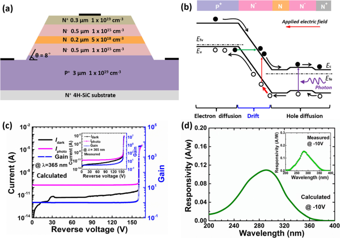
연구 방법 및 물리학 모델
그림 1a는 n
+
-기판으로 4H-SiC층을 사용합니다. 그런 다음 아키텍처 스택은 3μm 두께의 p
+
-유형 레이어(N아 =1 × 10
19
cm
−3
) p형 오믹접촉층 역할을 하는 0.5μm 두께의 n
-
-유형 곱셈 레이어(Nd =1 × 10
15
cm
−3
) 캐리어 곱셈을 위해 0.2μm 두께의 n형 전하 제어층(Nd =5 × 10
18
cm
−3
) 충격 이온화 프로세스를 종료하기 위한 0.5μm 두께의 n
−
-타입 흡수층(Nd =1 × 10
15
cm
−3
) 들어오는 광자를 흡수합니다. 장치 구조 상단에는 0.3μm 두께의 n
+
-타입 오믹접촉층(Nd =1 × 10
19
cm
−3
). 양의 경사각(θ =8°)는 에지 파괴를 억제하기 위해 메사 구조에 대해 생성됩니다[22, 23]. 4H-SiC SACM APD의 직경은 800 μm입니다. 캐소드 및 애노드 접점은 모두 우리의 계산에서 이상적인 옴 접점으로 간주됩니다. 그림 1c와 d에 따르면 우리의 결과는 앞서 언급한 표준 4H-SiC SACM APD 구조에 대한 계산 결과가 2.5 nA/cm
2
의 암전류를 나타냄을 보여줍니다. , 161.6 V의 항복 전압, 280 nm의 파장에서 0.11A/W의 피크 응답도. 표준 4H-SiC SACM APD에 대해 계산된 전류-전압 특성 및 응답성은 실험 데이터와 일치합니다. 이는 본 연구에서 사용된 충격 이온화, 4H-SiC 물질 흡수 계수, 푸아송 방정식, 전류 연속 방정식, 드리프트-확산 방정식이 합당하다는 것을 충분히 증명한다. 여기에서는 그림 1a의 구조를 연구 벤치마크로 사용하고 조사 변수에는 경사 메사 각도, 두께 및 각 레이어의 도핑 농도가 포함됩니다.
<그림>
아 개략적인 단면 구조(축척으로 그려지지 않음), b 표준 4H-SiC SACM APD, c에 대한 역 바이어스 하에서의 개략적인 에너지 밴드 다이어그램 계산된 전류-전압 특성 및 곱셈 이득 및 d 표준 4H-SiC SACM APD에 대해 10 V의 역 전압에서 계산된 스펙트럼 응답 특성. c의 삽입 그림 측정된 전류-전압 특성과 곱셈 이득을 보여줍니다. d의 삽입 그림 − 10 V
에서 바이어스된 표준 4H-SiC SACM APD에 대한 측정된 스펙트럼 응답 특성을 보여줍니다.
4H-SiC SACM APD의 광전 특성에 대한 다양한 구조적 변수의 영향을 더 잘 이해하기 위해 그림 1b는 역 바이어스에서 개략적인 에너지 밴드 다이어그램을 보여줍니다. 흡수층에서 생성된 전자-정공 쌍은 전하 제어층을 거쳐 증배층으로 확산됩니다. 광 생성 전자-정공 쌍이 증배 영역에 도달한 후 고갈된 전기장에 의해 분리됩니다. 그러면 홀은 증배층에서 증배 프로세스를 경험하여 내부 전류 이득을 발생시킵니다. 한편, 광 생성된 전자는 음극으로 돌아가 충격 이온화를 겪지 않고 전류로 변환됩니다. 광전류에 영향을 미치는 중요한 요소에는 증배층의 전기장 프로파일, 전하 제어층, 흡수층, n형 오믹 접촉층의 에너지 밴드 정렬이 포함되며, 여기서 에너지 장벽은 캐리어 수송을 방해할 수 있습니다. 증배층의 전기장 프로파일은 증배층과 전하 제어층 모두에 대한 도핑 농도에 의해 결정될 수 있다는 점도 주목할 가치가 있습니다. 한편, 베벨 메사 각은 또한 전기장 분포와 실질적으로 관련이 있습니다. 또한 고효율 캐리어 확산 공정을 보장하기 위해 각 층의 두께에 주의를 기울일 것입니다. 따라서 장치 성능을 최적화하기 위해 이러한 주요 구조적 매개변수를 체계적으로 연구하는 것이 중요합니다.
수치적 조사는 현재 연속성 방정식, 푸아송 방정식, 드리프트-확산 방정식을 적절한 경계 조건으로 일관되게 풀 수 있는 APSYS에서 수행됩니다. 충격 이온화 및 제너 터널링 프로세스는 모두 드리프트-확산 방정식에 포함되었습니다. 캐리어 수송 프로세스를 위한 캐리어-캐리어 산란은 낮은 필드 이동성 모델에도 포함되었습니다. Shockley-Read-Hall(SRH) 재결합 수명은 1 μs로 가정됩니다[24]. 특히 필드(E ) 전자에 대한 충격 이온화 계수의 의존성(αn ) 및 구멍(βp ) 4H-SiC 기반 층의 경우 Chynoweth 공식 (1) 및 (2)로 각각 다음과 같이 표현될 수 있습니다[25].
수치 모델에 사용된 다른 재료 매개변수는 다른 곳에서 찾을 수 있습니다[27]. 계산은 유한 요소법을 기반으로 하므로 정확한 계산을 위해 사용자가 메쉬 분포를 적절하게 조정해야 합니다.
결과 및 토론
n형 옴 접촉층에 대한 구조적 매개변수가 광전 성능에 미치는 영향
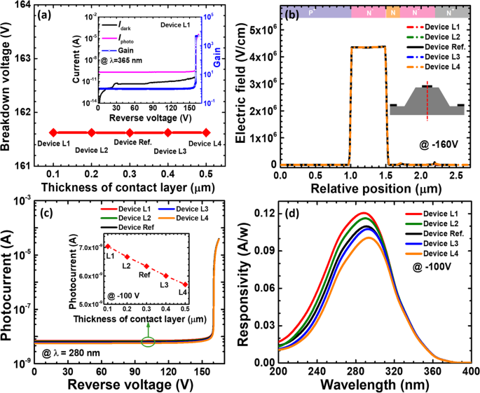
n형 저항성 접촉층의 두께와 도핑 농도가 광전 성능에 미치는 영향을 조사하기 위해 기준 소자, 소자 L1~L4, 소자 A1~A4를 각각 설계합니다. 참조 장치는 그림 1a와 같이 기본 SACM APD 구조입니다. 다른 제안된 APD는 n-형 SiC 옴 접촉층을 제외하고 기준 장치와 동일하며, 이에 대한 자세한 구조 정보는 표 1에 나와 있습니다.
먼저 그림 2a의 n형 SiC 저항성 접촉층, 즉 소자 L1~L4의 두께에 따른 항복 전압을 보여줍니다. 그림 2a의 삽입은 암전류, 365 nm 조명하의 광전류 및 장치 L1의 이득을 선택적으로 보여줍니다. 장치 L1의 경우 항복 전압은 ~ 161.6 V이고 암전류 밀도는 ~ 2.5 nA/cm
2
수준으로 유지됩니다. 바이어스가 161.6 V보다 낮을 때. 항복 전압은 10
−5
의 전류에서 얻어집니다. A. 임팩트 이온화 과정이 발생하면 암전류가 증가합니다. 광전류 레벨은 365nm 조명이 장치에 비출 때 선형 영역에서 높아지며 이는 곱셈 이득이 10
3
이상일 수 있음을 보여줍니다. 161.6 V의 역전압에서 장치 L1에 대해 조사된 5개의 APD에 대한 애벌랜치 항복 전압이 그림 2a에 요약되어 있습니다. 그림 2a에서 n형 저항성 접촉층의 두께가 항복 전압에 미치는 영향은 무시할 수 있음을 알 수 있습니다. 관찰에 대한 기본 메커니즘을 밝히기 위해 우리는 그림 2b에서 기준 장치 및 장치 L1~L4에 대한 수직 전계 분포를 계산하고 표시합니다. 이는 전하 제어 층이 공핍 영역과 전기장의 경계를 제한한다는 것을 보여줍니다. 곱셈 계층. 따라서 n형 오믹접촉층이 증배층의 전계 프로파일에 영향을 미치지 않을 것이라고 추측할 수 있으며 이는 그림 2b에서 입증되었습니다. 그림 2b의 관찰 결과는 그림 2a의 동일한 항복 전압을 기준 장치와 장치 L1~L4에 대해 잘 해석합니다. 다음으로, 우리는 그림 2c에서 5개의 장치에 대한 광 생성 전류를 보여줍니다. 더 나은 분해능을 위해 100 V의 바이어스에서 광 생성 전류를 수집합니다. 이는 그림 2c의 삽입도에 나와 있습니다. n형 저항성 접촉층의 두께가 증가함에 따라 광 발생 전류가 감소함을 알 수 있다. 너무 두꺼운 n형 옴 접촉층은 광 생성 캐리어가 비방사성 재결합을 일으키고 이에 따라 확산 전류를 감소시킵니다. 광 생성 전류를 사용하여 그림 2d에서 역전압 100 V에서 기준 장치 및 장치 L1~L4에 대한 스펙트럼 응답성을 얻을 수 있습니다. 5개의 조사된 장치에 대한 피크 응답 파장은 280 nm에 집중되어 있습니다. 응답성은 n형 접촉층의 두께가 증가함에 따라 감소하며, 이는 그림 2c의 삽입과 일치합니다. 따라서 n형 4H-SiC 저항성 접촉층의 두께는 비방사성 재결합 증가와 확산 전류 감소를 피하기 위해 적절하게 얇아야 한다고 요약합니다.
<그림>
아 항복 전압, b - 160 V로 바이어스된 SACM APD의 수직 전기장 분포, c 280 nm 조명에서 광전류-전압 특성 및 d n형 저항성 접촉층의 두께가 다른 기준 소자 및 소자 L1~L4에 대해 - 100 V로 바이어스된 SACM APD의 스펙트럼 응답 특성. a의 삽입 그림 계산된 전류-전압 특성 및 장치 L1에 대한 곱셈 이득을 보여줍니다. c의 삽입 그림 − 100 V
에서 바이어스된 기준 소자 및 소자 L1 ~ L4에 대한 광전류를 보여줍니다.
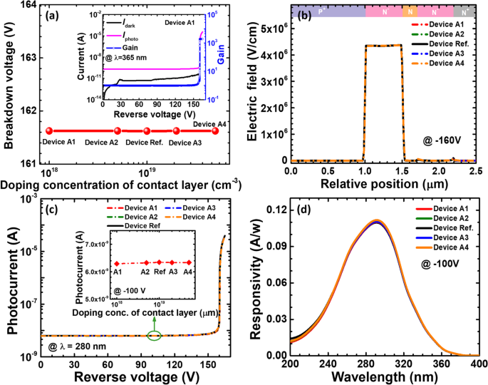
다음으로 그림 3a의 기준 소자와 소자 A1~A4를 분석하여 n형 저항성 접촉층의 도핑 농도에 따른 항복 전압을 조사합니다. 그림 3a의 삽입은 장치 A1에 적용된 바이어스 측면에서 암전류, 광 생성 전류 및 이득을 나타냅니다. 항복 전압은 전류가 10
−5
에 도달할 때 정의됩니다. A. 그림 3a에 따르면 항복 전압은 n형 4H-SiC 저항성 접촉층의 도핑 농도에 거의 의존하지 않습니다. 앞서 설명한 바와 같이 전하 제어층은 공핍 영역과 증배층의 전기장을 효과적으로 제한할 수 있습니다. 따라서 n형 오믹접촉층의 도핑 농도 변화는 소자 내부의 전계 분포에 영향을 미치지 않는다[그림 3b 참조]. 그런 다음 그림 3c의 기준 장치 및 장치 A1~A4에 적용된 바이어스 측면에서 광 생성 전류를 계산하고 표시합니다. 그림 3c에서 n형 저항성 접촉층의 도핑 농도가 바이어스된 광전류에 미치는 영향은 무시할 수 있음을 알 수 있습니다. 5개의 조사된 장치에 대한 서로 다른 파장에서의 스펙트럼 응답은 그림 3d에 나와 있습니다. 데이터는 100 V의 역전압에서 계산됩니다. 최대 응답도가 ~ 0.11A/W인 파장은 280 nm입니다. 도 3c와 일관되게, n형 오믹접촉층의 도핑 농도에 덜 의존하는 반응성을 알 수 있다. 따라서 우리는 4H-SiC SACM APD용 n형 저항성 접촉층의 도핑 농도보다 반응성이 두께의 영향을 더 많이 받는다는 결론을 내렸습니다. 또한 응답성을 향상시키기 위해 캐리어 확산 길이를 늘리는 것이 좋습니다.
<그림>
아 항복 전압, b - 160 V로 바이어스된 SACM APD의 수직 전기장 분포, c 280 nm 조명에서 광전류-전압 특성 및 d n형 저항성 접촉층의 도핑 농도가 서로 다른 기준 소자 및 소자 A1~A4에 대해 - 100 V로 바이어스된 SACM APD의 스펙트럼 응답 특성. a의 삽입 그림 장치 A1에 대한 계산된 전류-전압 특성 및 곱셈 이득을 보여줍니다. c의 삽입 그림 − 100 V
에서 바이어스된 기준 소자 및 소자 A1~A4에 대한 광전류를 보여줍니다.
흡수층의 구조적 매개변수가 광전 성능에 미치는 영향
이 섹션에서는 4H-SiC 기반 SACM APD의 광전 성능에 대한 흡수층의 두께와 도핑 농도의 영향을 연구합니다. SACM APD에 대한 흡수층의 자세한 구조 정보는 표 2에 요약되어 나와 있습니다. 장치 M1~M4 및 장치 B1~B4는 흡수층을 제외하고 구조적으로 참조 장치와 동일합니다. 소자 M1 ~ M4는 두께가 다른 반면 소자 B1 ~ B4는 흡수층에 대한 다양한 도핑 농도를 가지고 있습니다.
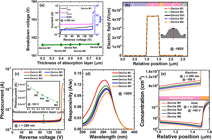
참조 장치 및 장치 M1~M4를 사용하여 그림 4a는 흡수층의 다양한 두께 측면에서 항복 전압을 보여줍니다. 시연을 위해 그림 4a의 삽입된 장치 M1에 적용된 바이어스의 함수로 암전류, 광 생성 전류 및 이득을 계산하고 표시합니다. 전류가 10
−5
일 때 항복 전압을 수집합니다. A. 내압이 흡수층의 두께에 거의 의존하지 않음을 알 수 있다. 항복 전압은 약하게 도핑된 증배층에서 전계 강도에 크게 영향을 받는 것으로 알려져 있으므로 그림 4b는 - 160 V의 역 바이어스에서 5개의 연구된 소자에 대한 수직 전계 분포를 보여줍니다. 참조 기기와 기기 M1~M4에 대한 필드 분포는 정확히 동일하므로 그림 4a의 결론을 확인합니다. 우리는 이후 그림에서 광 생성 전류와 응답성을 보여줍니다. 각각 4c 및 d. 광 생성 전류[그림 4c의 삽입 참조]와 응답성은 모두 흡수층의 두께가 증가함에 따라 감소하는 경향을 보여줍니다. 기본 메커니즘을 추가로 다루기 위해 5개의 조사된 장치에 대해 역 바이어스가 100 V일 때 그림 4e의 곱셈 계층 내 캐리어 분포를 계산하고 표시합니다. 우리는 흡수층의 두께가 증가함에 따라 전자와 정공 농도 수준이 모두 감소하는 것을 볼 수 있는데, 이는 흡수층이 두꺼워질 때 향상된 비방사성 재결합에 기인한다. 비방사성 재결합은 캐리어를 소모하여 확산 전류와 응답성을 억제합니다. 여기에서 비방사성 재결합에 의한 캐리어 소모를 피하기 위해 높은 검출율을 가진 4H-SiC SACM APD를 얻기에 흡수층이 너무 두꺼워서는 안 된다고 제안합니다.
<그림>
아 항복 전압, b - 160 V로 바이어스된 SACM APD의 수직 전기장 분포, c 280 nm 조명에서 광전류-전압 특성, d 스펙트럼 응답 특성 및 e - 100 V로 바이어스된 SACM APD의 증배층에서 캐리어 농도 프로파일은 흡수층의 두께가 서로 다른 기준 소자 및 소자 M1~M4에 대해 각각. a의 삽입 그림 계산된 전류-전압 특성과 장치 M1에 대한 곱셈 이득을 보여줍니다. c의 삽입 그림 − 100 V
에서 바이어스된 기준 소자 및 소자 M1~M4에 대한 광전류를 보여줍니다.
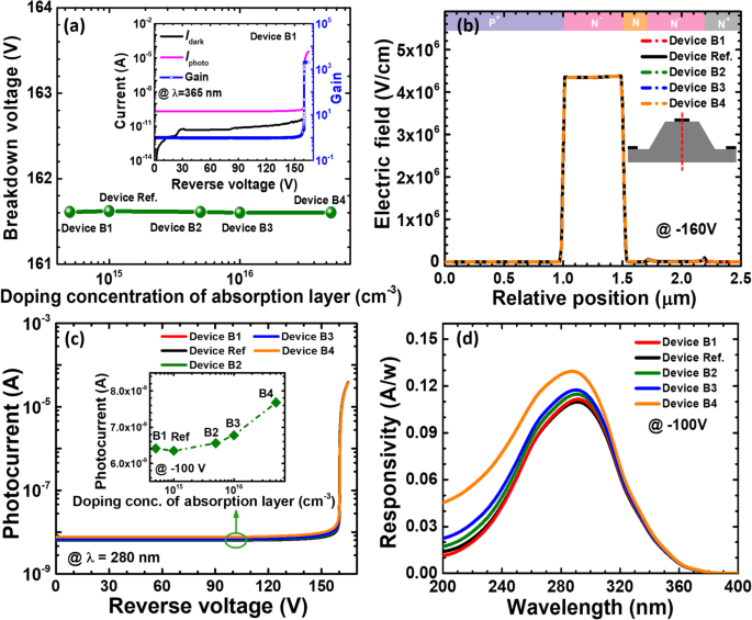
흡수층 두께 외에도 흡수층의 도핑 농도도 소자 성능에 상당한 영향을 미칩니다. 그런 다음 그림 5a의 참조 장치 및 장치 B1~B4에 대한 항복 전압을 계산하고 표시합니다. 항복 전압은 전류가 10
−5
일 때 정의됩니다. 그림 5a의 삽입에 표시된 대로 A. 그림 5에서 흡수층의 도핑 농도는 항복 전압에 큰 영향을 미치지 않음을 알 수 있습니다. 흡수층의 도핑 농도가 증배층의 전기장 프로파일을 크게 변경하지 않도록 그림 5b의 수직 1차원 전기장 분포에 의해 추가로 입증될 수 있습니다. 우리는 또한 그림 5c에서 연구된 장치에 대해 280 nm의 파장에서 광 발생 전류를 제시합니다. 이는 흡수층의 도핑 농도가 증가할 때 향상된 광 발생 전류를 나타냅니다. 그림 5c와 잘 일치하며 그림 5d의 파장 의존적 응답도는 흡수층(예:장치 B4)의 도핑 농도가 증가함에 따라 선호됩니다.
<사진>
아 항복 전압, b - 160 V로 바이어스된 SACM APD의 수직 전기장 분포, c 280 nm 조명에서 광전류-전압 특성 및 d - 100 V로 바이어스된 SACM APD의 스펙트럼 응답 특성은 흡수층의 도핑 농도가 서로 다른 기준 소자 및 소자 B1~B4에 대해 각각. a의 삽입 그림 계산된 전류-전압 특성과 장치 B1에 대한 곱셈 이득을 보여줍니다. c의 삽입 그림 − 100 V
에서 바이어스된 기준 소자 및 소자 B1~B4에 대한 광전류를 보여줍니다.
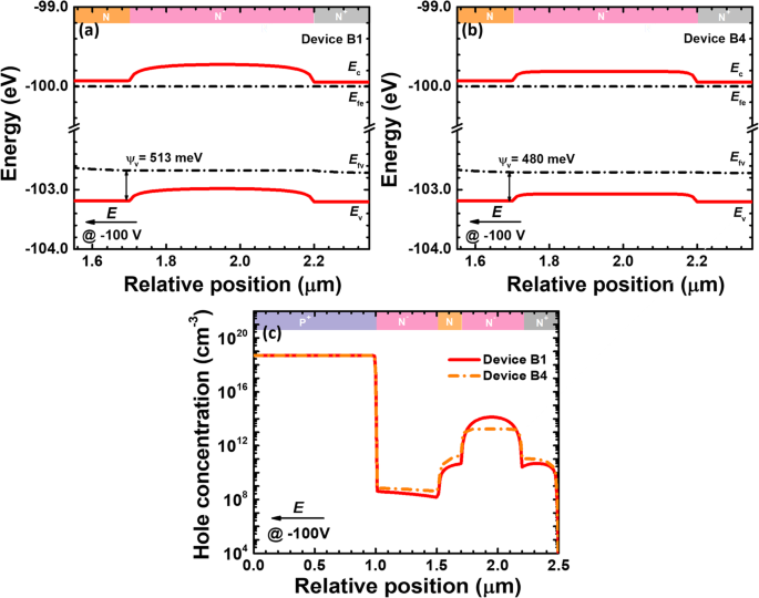
소자 B4에 대한 향상된 반응성에 대한 심층적인 기원을 보여주기 위해, 우리는 그림 1과 그림 B4에 소자 B1과 B4에 대한 전하 제어층, 흡수층, n형 오믹 접촉층에 대한 에너지 밴드 프로파일을 보여줍니다. 각각 6a 및 b. 여기서 전하제어층과 n형 오믹접촉층의 도핑 농도가 5 × 10
18
임을 언급할 가치가 있다. cm
−3
및 1 × 10
19
cm
−3
, 각각. 따라서 흡수층에 대한 더 낮은 도핑 농도는 내장 전기장을 생성하고 전하 제어층/흡수층/n형 오믹 접촉층의 계면에서 에너지 장벽을 생성할 수 있습니다[28]. 에너지 장벽은 광 생성 캐리어가 증배층으로 확산되는 것을 지연시킬 수 있습니다. 장벽을 줄일 수 있는 매우 편리한 방법은 흡수층의 도핑 농도를 높이는 것입니다. 결과적으로 유효 가전자대 장벽 값 ψv 전하 제어 층의 경우 소자 B1 및 B4의 경우 각각 513 meV 및 480 meV입니다. 흡수층에 대한 증가된 도핑 농도는 광 생성 정공의 수송을 촉진한다는 것이 목격됩니다[그림 6c 참조]. 충격 이온화는 더 많은 광 생성 정공이 증배 영역에 주입될 수 있게 되면 강해질 것이며, 이에 따라 광 생성 전류와 응답성이 증가합니다.
<그림>
a에 대한 전하 제어층, 흡수층 및 n형 저항성 접촉층의 에너지 밴드 다이어그램 장치 B1 및 b 장치 B4, c 장치 B1 및 B4에 대한 280 nm 조명 하에서의 홀 농도 프로파일. 데이터는 100 V의 역전압
에서 계산됩니다.
전하 제어층의 구조적 매개변수가 광전 성능에 미치는 영향
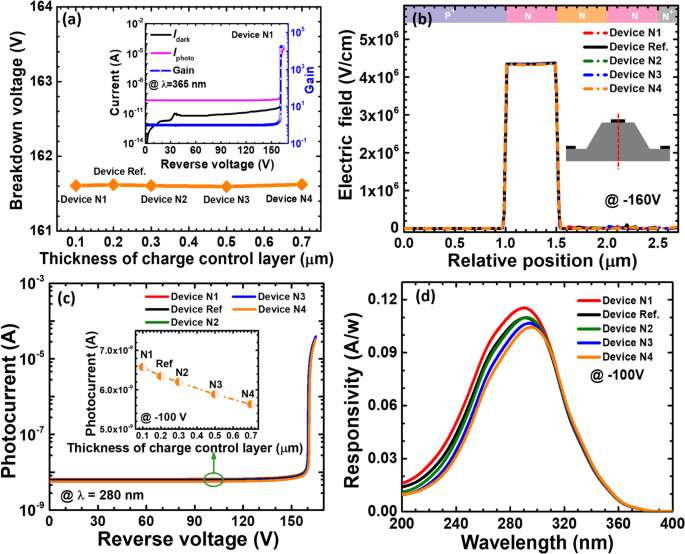
전하 제어층의 두께와 도핑 농도가 광전 성능에 미치는 영향을 조사하기 위해 표 3과 같이 전하 제어층에 대해 서로 다른 아키텍처 정보를 설정했습니다. 장치 N1~N4 및 장치 C1~C4는 기준 장치와만 다릅니다. 전하 제어 층에서. 장치 N1 ~ N4 및 C1 ~ C4에 대해 서로 다른 도핑 농도와 층 두께가 채택되었습니다.
앞에서 언급했듯이 충돌 이온화 및 애벌랜치 브레이크다운을 가능하게 하는 전기장은 주로 증배층에 국한됩니다. 그림 7a에서 전하 제어층의 두께에 따른 항복 전압은 전하 제어층의 두께가 캐리어 증배 과정에 아주 약간의 영향을 미친다는 것을 추론합니다. 이것은 도 7b를 보여줌으로써 더 증명된다. 그림 7c는 기준 장치 및 장치 N1~N4에 적용된 바이어스 측면에서 광 생성 전류를 보여줍니다. 전하 제어층의 두께가 증가하면 광 발생 전류가 낮아지며, 이는 또한 전하 제어층의 두께가 증가함에 따라 응답성이 작아지는 것으로 해석됩니다. 우리는 또한 캐리어를 소비하고 확산 전류를 억제하는 향상된 비방사성 재결합에 기인합니다.
<그림>
아 항복 전압, b - 160 V로 바이어스된 SACM APD의 수직 전기장 분포, c 280 nm 조명에서 광전류-전압 특성 및 d - 100 V로 바이어스된 SACM APD의 스펙트럼 응답 특성은 각각 다른 두께의 전하 제어층을 갖는 기준 소자 및 소자 N1 ~ N4에 대한 것입니다. a의 삽입 그림 계산된 전류-전압 특성과 장치 N1에 대한 곱셈 이득을 보여줍니다. c의 삽입 그림 − 100 V
에서 바이어스된 기준 소자 및 소자 N1 ~ N4에 대한 광전류를 보여줍니다.
전하 제어층의 역할은 강한 전기장과 캐리어 증배 과정을 증배층 내에 가두는 것입니다. 그러나, 전하 제어층의 도핑 농도가 감소하는 한, 공핍 영역의 폭은 더 확장될 수 있다. 그러면 전기장 프로파일은 항복 전압, 광 생성 전류, 이득 및 응답성에 실질적으로 영향을 미칠 수 있습니다. 따라서 우리는 표 3의 장치 C1 ~ C4를 설계합니다. 그림 8a에 따르면 도핑 농도가 감소함에 따라 초기에는 항복 전압이 동일하게 유지되고 전하 제어층에 대한 도핑 농도가 2 미만일 때 항복 전압이 증가합니다. × 10
18
cm
−3
. 그림 8a의 삽입은 항복 전압이 장치 C1에 대해 ~ 315 V이고 암전류도 3.5 × 10
−11
으로 상승함을 나타냅니다. A는 장치 N1에 대한 것과 비교됩니다. 그림 8a에서 관찰의 원점을 밝히기 위해 그림 8b에서 수직 전계 분포를 계산했는데, 이는 전기장이 주로 참조 장치 및 장치 C3 및 C4의 곱셈 층에 집중되어 있음을 보여줍니다. 그러나 전하제어층의 도핑 농도가 2 × 10
18
미만인 경우에는 전계와 공핍영역이 전하제어층으로 침투한다. cm
−3
. 소자 C1 및 C2에 대한 공핍 영역의 확장은 전계 강도를 감소시키는 데 도움이 되며 따라서 소자 C1 및 C2에 대한 항복 전압이 상응하게 증가합니다. 증가된 공핍 영역 너비는 더 많은 공간 전하 생성 전류를 생성하므로 암전류가 증가합니다(즉, 3.5 × 10
− 11
). A 및 5 × 10
− 11
A는 각각 장치 C1 및 C2에 대한 것입니다. 그런 다음 그림 8c에 280 nm의 파장에서 광 발생 전류를 보여줍니다. The 100V-biased spectral responsivity curves at different wavelengths for the five investigated devices are illustrated in Fig. 8d. Excellent agreement is obtained between Figs. 8c and d, such that the increased photo-generated current gives rise to the enhanced responsivity, i.e., devices C1 and C2. Other devices show similar photo-current level and the responsivity.
아 Breakdown voltage, b vertical electric field distribution of the SACM APDs biased at − 160 V, c photocurrent biased at − 100 V, and d spectral response characteristics of the SACM APDs biased at − 100 V for reference device and devices C1 to C4 with different doping concentration of charge control layer, respectively. Inset figure in a shows the calculated current-voltage characteristics and the multiplication gain for device C1. Inset figure in c shows photocurrent-voltage characteristics for reference device and devices C1 to C4
As has been interpreted previously, the energy band barrier height at the interface of multiplication layer/charge control layer can soundly affect the carrier diffusion. Due to the expansion of the depletion region for devices C1 and C2, the electric field in the depletion region will annihilate the energy barrier at the interface of multiplication layer/charge control layer [e.g., the inset for device C1 in Fig. 9a]. Meanwhile, we observe the valence band barrier at the interface of multiplication layer/charge control layer for device C4 according to the inset for Fig. 9b. The energy barrier will correspondingly retard the hole diffusion into the multiplication layer from the charge control layer. We also selectively compute and show the hole concentration profiles for device C1 and C4 in Fig. 9c. Because the interface of multiplication layer/charge control layer for device C1 no longer hinders the injection of photo-generated holes into the multiplication layer, more holes are limited in the charge control layer and the absorption layer for device C4. As a result, the hole concentration in the multiplication layer for device C1 is higher than that for device C4. Thus, the enhanced photo-generated current and the responsivity for device C1 are obtained when compared with device C4.
Energy band diagrams for a device C1 and b device C4, c hole concentration profiles for device C1 and C4. Data are calculated at the reverse voltage of 100 V. Insets for a 그리고 b show the local energy band diagrams for multiplication layer/charge control layer for devices C1 and C4, respectively
Impact of the Structural Parameters for the Multiplication Layer on the Photoelectric Performance
The impact ionization and the carrier multiplication process take place in the multiplication layer, making the design for the multiplication layer essentially vital for 4H-SiC SACM APDs. Therefore, we look into the impact of the thickness and doping concentration for the multiplication layer on the photoelectric performance for SACM APDs. The detailed structural information of the multiplication layer for different SACM APDs are summarized and presented in Table 4. The only difference for the devices in Table 4 lies on the multiplication layer.
As Fig. 10a presents, the breakdown voltage is enhanced from 110 to 210 V when the multiplication layer thickness is increased from 0.3 to 0.7 μm. For the purpose of demonstration, the inset of Fig. 10a demonstrates the current in terms of the voltage for reference device and devices P1 to P4. This indicates that a thick multiplication layer helps to reduce the electric field intensity [see Fig. 10b] and increase the breakdown voltage. We then show the photo-generated current for the five devices in Fig. 10c. The photo-generated current increases slightly with increasing the thickness of the multiplication layer for devices P2 to P4, except that device P1 has the highest photocurrent. The spectral responsivity characteristics for the five investigated devices at the reverse voltage of 100 V are provided in Fig. 10d. The peak responsivity for reference device and devices P2 to P4 improves slightly as the thickness of the multiplication layer increases, and this is because the number of carriers generated by impact ionization increases when the depletion region width increases. Note that device P1 with the thinnest multiplication layer owns the highest peak responsivity at the wavelength of 280 nm. This is because the − 100 V applied voltage is close to Geiger mode for device P1, and the avalanche gain is more likely to occur than that for other devices.
아 Breakdown voltage, b vertical electric field distribution of the SACM APDs biased at − 160 V, c photocurrent biased at − 100 V, and d spectral response characteristics of the SACM APDs biased at − 100 V for reference device and devices P1 to P4 with different thicknesses of multiplication layer, respectively. Inset figure in a shows the calculated current-voltage characteristics for reference device and devices P1 to P4. Inset figure in c shows photocurrent-voltage characteristics under 280 nm illumination for reference device and devices P1 to P4
Then, we show the breakdown voltage in terms of the multiplication layer doping concentration for reference device and devices D1 to D4 in Fig. 11a. It seems that when the doping concentration for the multiplication layer is lower than 10
16
cm
−3
, the breakdown voltage is less affected. We believe the breakdown voltage can be significantly decreased if the doping concentration in the multiplication layer exceeds 10
18
cm
−3
. The dark current as a function of the applied bias for the five APDs are shown in the inset of Fig. 11a. The dark current increases with increasing doping concentration of the multiplication layer due to the enhanced space charge generation in the depletion region. Therefore, for the purpose of significantly decreasing the dark current and promoting the carrier multiplication process, we rarely have the multiplication layer heavily doped. Then, we calculate the vertical one-dimensional electric field profiles for the five studied devices, which are demonstrated in Fig. 11b. We can see that the electric field profiles of the five devices are mainly confined in the multiplication layer. In addition, Figs. 11c and d demonstrate the photo-generated current and the wavelength-dependent responsivity for the five devices. We can see that the photo-generated current for reference device and devices D1 and D2 are almost the same under the 280 nm illumination, while that the photon-generated current for the devices D3 and D4 is slightly increased. Therefore, the responsivity at the wavelength of 280 nm in Fig. 11d for devices D3 and D4 is slightly higher than the others.
아 Breakdown voltage, b vertical electric field distribution of the SACM APDs biased at − 160 V, c photocurrent-voltage characteristics under 280 nm illumination, and d spectral response characteristics of the SACM APDs biased at − 100 V for reference device and devices D1 to D4 with different doping concentration of multiplication layer, respectively. Inset figure in a shows the calculated current-voltage characteristics for reference device and devices D1 to D4. Inset figure in c shows photocurrent for reference device and devices D1 to D4 biased at − 100 V
Impact of the Beveled Mesa Angle on the Photoelectric Performance
In order to eliminate premature breakdown and suppress leakage current that are caused by the junction termination, positive beveled mesas with a small inclination angle are usually adopted when fabricating 4H-SiC APDs [13,14,15,16, 18]. However, the angles of the positive beveled mesa adopted in previous reports are various. Thus, to get systematic insight into the influence of different mesa inclination angles on the electric field profiles for 4H-SiC SACM APDs, we design the devices that are shown in Table 5.
We firstly calculate and show the dark current-voltage characteristics for the six investigated devices with the various bevel angles in Fig. 12a. We can see that the dark current increases as the positive beveled angle becomes large [see Fig. 12a]. The breakdown voltages for the investigated devices are ~ 161.6 V except that device E5 is slightly less than 161.6 V. The premature breakdown is observed as the beveled mesa angle increase in the dark condition. Meanwhile, we calculate and show photo-generated current in terms of the applied bias for reference device and devices E1 to E5 in Fig. 12b. We also see that the photo-generated current also increases as the positive bevel increases according to the inset for Fig. 12b. The premature breakdown is also observed as the beveled mesa angle increase in Fig. 12b. Therefore, the responsivity of solar-blind waveband at − 100 V slightly enhances as the positive bevel angle increases according to Fig. 12c.
아 Numerically calculated dark current-voltage characteristics, b photocurrent-voltage characteristics under 280 nm illumination, and c spectral response characteristics of the SACM APDs biased at − 100 V for reference device and devices E1 to E5, respectively
To reveal the origin for the observations in Figs. 12a and b, we calculate the lateral electric field distribution in the multiplication layer at the reverse bias of − 100 V in Fig. 13a, which demonstrates that, when the beveled mesas are utilized, the electric field decreases from the mesa center to the mesa edge. Moreover, the edge electric field intensity drops as the angle further decreases for the investigated devices. As has been mentioned, the junction termination will cause a large number of surface imperfections, which may cause the premature breakdown and the strongly leakage current, and the adopting of the beveled mesa shifts the premature breakdown from the mesa surface to the bulk [29]. Moreover, to get a full picture for the electric field profiles, the two-dimensional electric field distributions at the reverse bias of − 100 V for reference device and devices E1 to E5 are presented in Figs. 13b-g. We can see that the area of the high electric field in the entire multiplication layer gets narrowed, and this simultaneously causes the carriers that regenerated by impact ionization to decrease. As can be seen from Table 6, as the beveled mesa angle decreases, the surface electric field at the relative position of 700 μm decreases from 2.03 × 10
6
V/cm to 2.90 × 10
5
V/cm. As a result, the surface leakage and bulk leakage can be further suppressed as the beveled mesa angle get further decreased as shown in Fig. 12a. Although a small beveled mesa angle is preferred, this sacrifices the active detection area for APDs, and therefore, the responsivity is the lowest for device E1 according to Fig. 12c. Thus, one shall properly optimize beveled mesa angles depending on the crystalline quality for the 4H-SiC epitaxial layers and the surface conditions after junction termination. The suggested beveled angle in this works is in the range of 10–20°.
아 Lateral electric field distribution of the multiplication layer at − 100 V, and numerically calculated two-dimensional electric field distribution at − 100 V for b device E1, c reference device, d device E2, e device E3, f device E4 and g device E5
결론
To summarize, we have numerically investigated and demonstrated the impact of the thickness and doping concentration of each layer on photoelectric performance for 4H-SiC SACM APDs. The obtained conclusions are as follows:(1) for n-type ohmic contact layer with a properly high doping concentration (Nd ≈ 1 × 10
19
cm
−3
) to enable ohmic contact, the thickness and doping concentration hardly affect the breakdown voltage. Nevertheless, the responsivity decreases as the thickness of the n-type ohmic contact layer increases. The thickness shall be controlled to about 0.2 μm; (2) the doping concentration for the absorption layer is vitally important, which can modulate the photo-generated carrier transport and affect the responsivity. The doping concentration is generally controlled at the intrinsic concentration (Nd ≈ 1 × 10
15
cm
−3
); (3) the doping concentration for the charge control layer regulates the electric field distribution and affects the depletion region width for 4H-SiC SACM APDs. The depletion region width increases as the doping concentration of the charge control layer decreases. According to our results, when the doping concentration is about 1 × 10
18
cm
−3
, the depletion region can be completely terminated by the charge control layer; (4) the breakdown voltage can be strongly affected by the thickness of multiplication layer which is the main support region of the electric field. The dark current is sensitive to the doping concentration of multiplication layer, and a low doping concentration for the multiplication layer is required, since the doping concentration therein influences the space charge generation current. Thus, the suggested doping concentration in this works is intrinsic concentration (Nd ≈ 1 × 10
15
cm
−3
); (5) we also point out the advantage of beveled mesa for 4H-SiC SACM APDs, and the optimized beveled mesa angles shall be a compromise among the active detection area, the surface conditions for the mesa, and the crystalline quality for 4H-SiC epitaxial films. This work indicates that the optimum beveled mesa angle is in the range of 10–20°. We strongly believe that this work provides the physical insight for the device physics and hence the findings in this work are very important for 4H-SiC-based SACM APDs.
데이터 및 자료의 가용성
The data and the analysis in the current work are available from the corresponding authors on reasonable request.