

산업기술

산업 제조
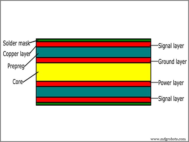
다층 풀에서 인쇄 회로 기판에는 다양한 레이어가 있습니다. 계층은 틈새 시장에 완전히 예리하고 정통하지 않은 사람들을 혼란스럽게 할 수 있습니다.
빠르게 제작된 대부분의 PCB 프로토타입은 2개의 레이어로 구성됩니다. 그러나 많은 전자 장치가 이층 기판에 국한되지 않습니다. 더 높고 정교한 보드가 필요합니다.
이 기사는 PCB 레이어와 그 작동 방식을 더 잘 이해하는 데 도움이 될 것입니다.
인쇄회로기판은 전달하고자 하는 메시지에 따라 의미가 다릅니다. PCB 레이어와 관련하여 특정 수량과 순서로 제공되는 구리 레이어라고도 설명합니다.
구리 레이어는 신호 레이어 또는 레이어라고 할 수 있습니다. PCB 레이어는 위치와 제공하는 기능에 따라 이름이 지정됩니다. 구리 층 수에 따른 PCB의 순위입니다.
예를 들어, 하나 또는 두 개의 레이어가 있는 보드는 각각 1레이어 PCB 또는 단면 PCB 및 2면 레이어 PCB 또는 단순히 양면 PCB라고 부를 수 있습니다.
PCB Layer에는 다양한 유형이 있으며 일반적인 것은 다음과 같습니다.
1. 기계 레이어
2. 오버레이 / 실크스크린 레이어
3. 라우팅 레이어
4. 솔더 마스크 레이어
5. 솔더 페이스트 레이어
6. 레이어 제외
7. 접지면과 동력면
8. 분할면
모든 PCB가 위에 열거된 모든 레이어로 구성되는 것은 아님을 기억하십시오. 디자인의 특성에 따라 다양한 레이어 유형의 필요성이 결정됩니다. 단일 레이어 보드는 일반적으로 6레이어 유형으로 구성됩니다.
여기에는 기계적, 킵 아웃, 라우팅, 오버레이, 솔더 마스크 및 솔더 페이스트 레이어가 포함됩니다.
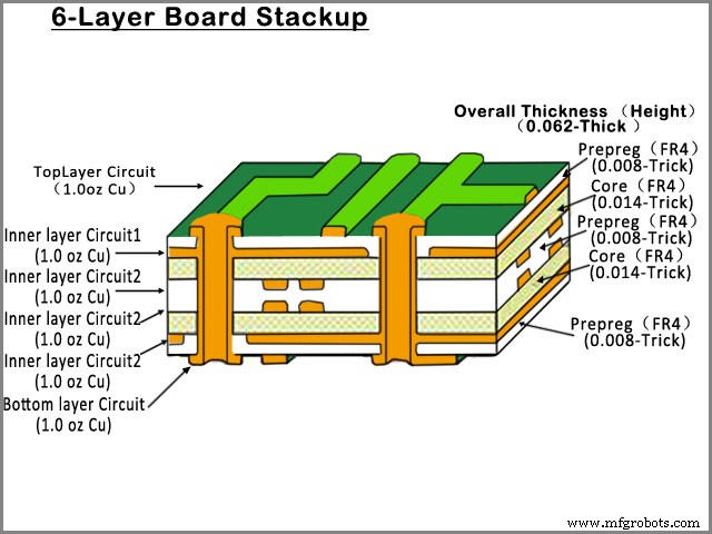
다층 PCB의 경우 6개의 레이어와 다른 발전소, 접지면, 추가 라우팅 레이어의 조합으로 구성됩니다.
2레이어, 4레이어, 6레이어 PCB가 가장 일반적인 기판이며, 12레이어 이상의 PCB를 갖는 것은 드문 일이 아닙니다.
여러 기계적 레이어가 있을 수 있지만 보드를 구성하려면 최소한 하나는 필요합니다. 가장 기본적인 기계적 레이어는 보드의 물리적 치수를 정의합니다.
기계 레이어는 기계 1이라고도 합니다. 제작자가 재료에서 회로 기판을 잘라낼 때 사용할 레이어입니다.
인쇄 회로 기판은 기판의 물리적 치수를 설명하는 단일 라우팅 레이어처럼 간단할 수도 있고 이 기사에서 언급한 모든 레이어를 포함하여 많은 레이어가 있는 기판처럼 복잡할 수도 있습니다.
반면에 개별적으로 고려하면 모든 단일 계층에는 특정 기능이 있습니다. 기판이 아무리 복잡해도 PCB 구성이 매우 간단해지기 때문에 각 레이어의 목적을 이해하는 것이 중요합니다.
이 프레임워크는 단순한 직사각형, 곡선 모서리가 있는 복잡한 모양 또는 컷아웃이 될 수 있습니다.
드물기는 하지만 더 많은 기계적 레이어가 포함되어 도구 사양 및 기타 추가 자동 정보를 지정합니다. 그러나 대부분의 인쇄 회로 기판에는 이러한 추가 기계적 레이어가 필요하지 않습니다.
레이어 스택업은 레이어 유형의 적절한 배치입니다. PCB는 일반적으로 세 가지로 분류됩니다.
위의 용어는 PCB의 구리 층 수를 설명합니다. 다층 PCB는 4, 6, 8 범위에서 2개 이상의 층이 있는 PCB를 나타냅니다.
다중 레이어에서 상단과 하단 레이어는 외부 레이어로 알려져 있고 그 사이에 있는 레이어는 내부 레이어로 알려져 있습니다. 다층 PCB 제조의 복잡성으로 인해 이중 및 단층 PCB에 비해 비용이 상당히 많이 듭니다.
레이어 스택에서 고려할 수 있는 몇 가지 사항이 있으며 여기에는 다음이 포함됩니다.
회로의 다른 설계에는 적절하게 적합한 다른 레이어 스택업이 있습니다. 레이어 스택업은 인쇄 회로 기판의 기능에 필수적입니다.
레이어 스택업이 잘 계획되지 않은 경우 다음과 같은 다양한 문제가 발생할 수 있습니다.
위의 문제와 그 이상을 피하려면 잘 계획된 PCB 레이어 스택을 만드는 것이 중요합니다. 효율적인 PCB 레이어 스택을 설계하여 많은 비용을 절감할 수 있으며, 이는 부적절한 설계로 인해 발생할 수 있는 문제를 방지하는 데 큰 도움이 됩니다.
Layer Stackup에서는 PCB 레이어 순서 외에 기판 재질, 구리 두께도 고려됩니다.
다양한 유형의 회로 설계에 대해 서로 다른 레이어 스택이 있습니다. 잘 계획된 PCB 레이어 스택은 전자기 간섭, 신호 누화, 결합, 오버슈트 및 언더슈트, 신호 손실 감소와 같은 PCB의 최상의 성능을 보장합니다.
완성할 설계와 처음으로 자격을 갖추면 비용과 설계 주기 시간을 크게 줄일 수 있습니다. 신호 무결성 문제가 발생하기 전에 제거된다면 가능합니다.
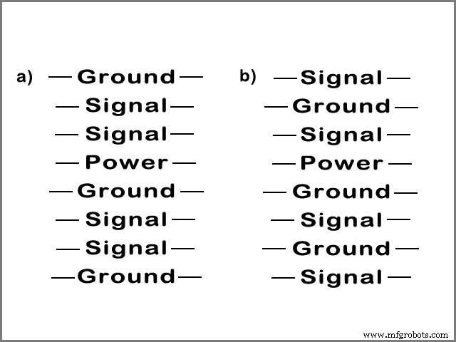
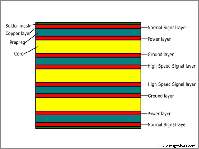
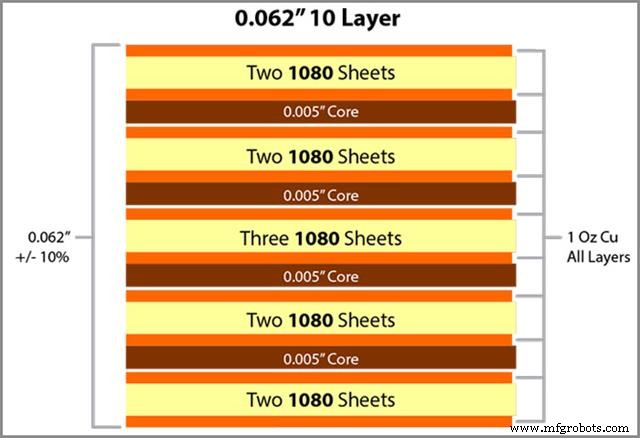
두 개의 8-레이어 아래 그림 1에는 레이어의 순서 변경을 강조하는 스택업 방식이 나와 있습니다.
신호 레이어 외에 파워 플레인도 성공적인 제품 개발에 중요한 역할을 합니다.
디지털 또는 아날로그 신호는 크로스토크를 줄이고 결과적으로 신호 무결성을 개선하는 마이크로스트립 라인 또는 스트립 라인을 통해 라우팅할 수 있습니다.
저주파 신호는 내부 레이어로 라우팅되고 고주파 신호는 외부 레이어로 라우팅됩니다.
각 신호 레이어에 인접하게 접지면 레이어를 배치하는 것이 좋습니다. 그러나 레이어 스택 업 및 제조 비용을 줄이기 위해 접지 레이어는 각각의 두 신호 레이어 뒤에 배치됩니다. 파워 플레인은 또한 긴밀한 결합을 만드는 접지 플레인에 인접해야 합니다.
전원 공급 장치 레일이 여러 개인 경우 전원 플레인은 둘 이상의 부품으로 분할됩니다. 일반적으로 PCB 두께는 1.6mm이지만 12겹 이상 1.6mm 두께를 유지하는 것은 어려운 일입니다.
2개의 8-레이어 아래의 그림 1은 레이어의 변화하는 순서를 강조하는 스택업 방식을 보여줍니다.
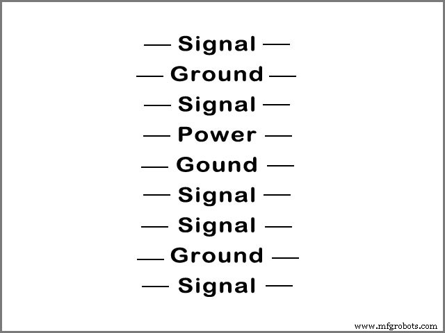
그림 2에서는 10-layer PCB Stackup 방식을 설명합니다.
이 두 용어가 같은 것을 의미하는 것처럼 보이지만 이것은 전혀 그렇지 않습니다. 위에 정의된 레이어 스택업은 레이어 유형의 적절한 배치입니다.
한편, PCB 레이어는 일정 수량과 순서로 제공되는 구리 레이어를 의미합니다. 레이어 스택업은 레이어 계획과 관련이 있는 반면 PCB 레이어는 레이어의 양과 순서와 관련이 있습니다.
종종 단일 레이어 PCB라고 하는 단일 레이어 PCB는 한 면에서 인쇄됩니다. 이것은 PCB 시트가 한 면에는 전도성 물질과 함께 있고 다른 면에는 전자 부품이 연결되어 있음을 의미합니다.
처음에는 모든 PCB를 수동으로 설계했지만 이제는 기술 발전으로 인해 Eagle PCB 소프트웨어와 같은 전문 소프트웨어를 사용하여 만들 수 있습니다. 이 프로그램이 있는 컴퓨터를 사용하여 수행됩니다.
단층 PCB는 다양한 유형으로 제공됩니다. 그 중 일부는 다음과 같습니다:
• 유연한 PCB. 이 단층 PCB는 단단한 재료 대신 유연한 재료로 만들어집니다. 이 경우 사용할 수 있는 재료에는 플라스틱이 포함됩니다. 이러한 유형의 단층 PCB는 생산 비용이 상당히 높아서 비경제적입니다.
• 경질 PCB. 이 단층 PCB는 유리 섬유와 같은 단단한 재료로 만들어집니다. 그들은 유연하지 않으므로 회로가 구부러지는 것을 허용하지 않습니다. 계산기, 전원 공급 장치 등과 같은 대부분의 장치에서 일반적으로 사용됩니다.
• 고주파 PCB의. 이 단층 PCB는 작동에 상당히 높은 주파수가 필요한 회로에 사용됩니다. 이러한 PCB에 사용할 올바른 재료를 선택할 때 열팽창, 수분 흡수 및 유전 손실이 고려되는 몇 가지 요소입니다.
• Rigid-Flex PCB. 이 단층 PCB는 플라스틱과 유리 섬유의 조합으로 만들어집니다. 두 재료 모두 단일 레이어로 결합됩니다. 이 조합은 결과적으로 PCB의 크기와 무게를 줄입니다.
• 알루미늄으로 뒷받침되는 PCB. 이 단층 PCB는 알루미늄 재질로 만들어집니다. 이 PCB의 디자인은 구리 PCB와 거의 유사하지만 사용된 물품에 차이가 있을 뿐입니다.
레이어 PCB는 보시다시피 매우 간단합니다. 그러나 그들의 단순함이 그들이 달성할 수 있는 것에 대해 당신을 속이지 않도록 하십시오. 그것들은 단순할 수 있지만 복잡한 장치에서 작업하는 것과 관련하여 많은 것을 생성합니다. 그들이 수행하는 몇 가지 기능이 있으며 그 중 일부는 다음과 같습니다.
단층 PCB에는 다음과 같은 몇 가지 장점이 있습니다.
2층 PCB는 2층 또는 양면 PCB라고도 합니다. 주로 FR-4 유리 에폭시 기판으로 양면에 얇은 구리 필름 또는 레이어를 적층합니다. 설계하기에 가장 간단하고 경제적인 PCB입니다.
2층 PCB는 전문 PCB 프로토타이핑 공장(예:wellpcb.com)에서 쉽게 제조하고 집에서 만들 수 있습니다. 2층 PCB는 상단과 하단 구리 레이어만 있습니다.
경제적인 것도 잊지 않고 생각해낼 수 있는 심플한 디자인입니다. 이 PCB 디자인은 올바른 소프트웨어를 사용하여 가정에서 쉽게 제조할 수 있습니다. 대부분 PCB 프로토타이핑 회사에서 만든 것입니다.
이 디자인의 PCB 레이어는 주로 상단 레이어를 형성하는 신호 레이어와 전기 부품으로 구성된 하단 레이어입니다. 이중층 PCB의 모든 구성 요소는 다음과 같습니다.
이중층 PCB가 사용되는 곳이 있습니다. 일부 적용 분야는 다음과 같습니다.
• 조명에서. 이중 레이어 PCB는 LED 조명에 사용되므로 전력이 필요합니다.
• 의료 기기에서. 이중층 PCB는 심박 조율기 및 CAT 검사기와 같은 의료 장비에 활용됩니다.
• 자동차 및 항공우주 산업. 자동차 산업과 항공 산업 모두에서 PCB는 많이 사용됩니다. 더 정확하게 말하면 양면 PCB는 주로 이 두 산업 분야에서 사용됩니다.
이중층 PCB에는 다양한 이점이 있습니다. 아래에서 그 중 일부를 살펴볼 수 있습니다.
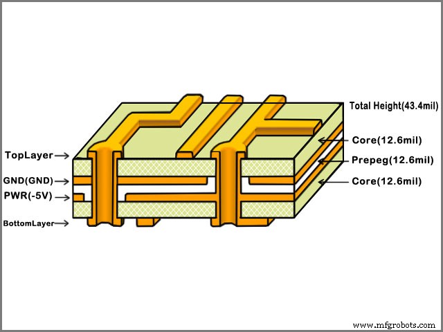
4층 PCB에는 4개의 구리층이 있습니다. 상단 및 하단 레이어는 라우팅 레이어이고 그 사이에 끼워진 두 레이어는 전원 및 접지면입니다.
Four-layer, PCB Copper 레이어 사이에는 Core와 Prepreg가 있습니다. 제조 과정에서 이러한 모든 요소는 높은 열과 압력에서 라미네이트로 결합(샌드위치)되어 전체 스택업이 함께 유지되도록 합니다.
4층 PCB는 관통 비아, 블라인드 비아 및 매립 비아를 포함할 수 있습니다. 4레이어 PCB의 경우, 매립 비아는 두 번째와 세 번째 레이어 사이에만 있을 수 있고 블라인드 비아는 상단(첫 번째)과 두 번째 레이어 사이 또는 하단(네 번째)과 세 번째 레이어 사이에 있을 수 있습니다. 피>
4레이어 보드의 일반적인 스택업은 내부 2개 레이어에 대한 전원 및 접지와 외부 2개 레이어에 대한 신호입니다. 하나는 일반적으로 두 신호 레이어를 수직으로 라우팅합니다.
레이어가 전원과 접지로 분리되어 있으면 중요하지 않지만 인접한 레이어에 신호가 있는 경우 누화를 최소화하는 것이 더 중요해집니다.
번호 매기기에 관해서는 일반적으로 1에서 n으로, 위에서 시작하여 아래로 내려갑니다. 이것이 유일한 규칙입니다. 프로덕션을 위해 파일을 보낼 때 누적 정보를 제공하므로 원하는 모든 작업을 수행할 수 있습니다.
4층 PCB 제조 시 제조 공장이 있는 경우 비용이 상당히 유용할 수 있습니다.
6층 PCB를 만드는 디자인은 내성이 있고 조용합니다. 6층 PCB가 다른 PCB에 비해 유리한 몇 가지 이유가 있습니다. 몇 가지 아이디어는 다음과 같습니다.
• 세 번째 레이어와 첫 번째 레이어 사이에 있는 트레이싱은 특별한 처리가 필요하지 않습니다.
• 모든 흔적은 지면과 가깝습니다.
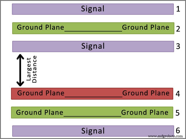
참조 평면은 반환 전류를 전송하는 데 사용됩니다. 4계층 설계에서 1계층은 2계층에 고주파 수익률 통화를 가지고 있고 4계층도 3계층에 빈도가 높습니다. 따라서 6층 PCB와 차이가 없습니다.
참조 평면을 라우팅 또는 신호 레이어에 더 가깝게 이동하면 방사 방출을 결정하는 루프 영역이 줄어듭니다. 그리고 고주파수에 대한 민감도.
다음은 6레이어 스택이 잘 작동하도록 하는 몇 가지 요소입니다.
1. 모든 흔적에 의한 지면과의 근접성.
2. 접지면과 플래너 커패시턴스를 생성하는 전력의 근접성.
3. 특별한 처리가 필요 없는 세 번째 레이어와 첫 번째 레이어 사이의 트레이싱.
4. 레이어 4 참조 평면이 레이어 2와 레이어 사이의 거리보다 높습니다.
최상의 6층 PCB 설계는 PCB에 있는 두 개의 접지면을 연결하기 위해 스티칭이 필요하며, 이 접지면은 전류를 기준면으로 되돌려 보내야 합니다. 어떤 사람들은 여분의 접지면을 추가하면 방출과 면역으로부터 보호하는 데 도움이 된다고 말합니다.
평면 절단은 방출과 민감성 모두에서 EMC에 치명적일 수 있습니다. 평면 절단 또는 보이드는 전원 또는 접지 평면이 평면의 주어진 부분을 통해 의도하지 않거나 의도적으로 절단된 경우입니다. 평면 컷은 다양한 크기와 모양으로 제공됩니다.
평면의 전류 반환 경로는 수천 인치 떨어져 있으며 좋은 설계에서는 트레이스가 평면에 인접하여 실행되므로 반환 전류 경로가 근처에 있도록 하여 루프 영역을 상대적으로 작게 형성합니다.
구리 평면 레이어에 일부 보이드를 도입할 때 보이드 및 평면 절단을 가로지르는 트레이스에 필요한 루프를 생성해야 합니다. 현재 루프 영역을 훨씬 더 중요하게 만듭니다.
8레이어 보드는 라우팅 레이어를 2개 더 추가하거나 플레인을 2개 더 추가하여 EMC 성능을 향상시킬 수 있습니다.
6층 기판에 비해 8층 기판의 비용 증가 비율은 4층에서 6층으로 증가하는 비율보다 적기 때문에 EMC 성능 향상을 위한 비용 증가를 더 쉽게 정당화할 수 있습니다.
따라서 대부분의 8층 기판은 4개의 배선층과 4개의 평면으로 구성됩니다.
일반적으로 8단 PCB를 만들기 위해서는 동층, 프리프레그, 코어의 교대로 층이 필요합니다. 프리프레그는 8층 PCB 스택업을 단일 기판으로 단단히 결합하는 접착제 역할을 합니다.
전자기 호환성을 개선하기 위한 규칙에 따라 간단한 8레이어 PCB 구성은 다음과 같습니다. 8계층 PCB는 높은 신호 무결성을 달성할 수 있습니다. 6단 PCB 이하와 비교.
신호 네트워크 수, 장치 밀도, PIN 밀도, 신호 주파수, 보드 크기에 따라 PCB 스택업 설계 방법을 선택할 수 있습니다. 신호 네트워크 수가 많을수록 장치 밀도가 높아집니다. PIN 밀도가 높을수록 신호가 높아집니다.
또한 우수한 EMI 성능을 위해서는 각 신호 레이어에 참조가 있는지 확인하는 것이 가장 좋습니다.
8층 PCB를 사용하면 몇 가지 장점이 있습니다. 장점과 이점은 다음과 같습니다.
• 중단으로 이어질 수 있는 전자기 간섭을 줄입니다.
• 신호 무결성을 향상시킵니다.
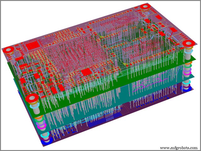
32개의 레이어로 구성된 다층 PCB일 뿐입니다. 레이어는 함께 결합되어 단일 PCB로 작동합니다. 이러한 PCB 레이어는 고급이므로 기술과 정밀도가 필요합니다.
PCB의 모든 설계는 소프트웨어에서 시작됩니다. 32 레이어 PCB의 경우 많은 PCB 레이어를 포함하는 스택업이 만들어집니다. 레이어를 함께 끼우는 기계를 사용하여 가능합니다.
32층 PCB를 사용하도록 선택할 수 있는 몇 가지 이유가 있습니다. 몇 가지 아이디어는 다음과 같습니다.
• 항공 우주 시스템에 사용됩니다.
• 자동차 분야에서 사용.
32레이어 PCB 이면의 기술
32 Layer PCB를 제작하기 위해 여러 개의 PCB Layer로 구성된 Stack-Up을 구성합니다.
모든 두 개의 이중층 PCB 사이에 절연 섬유-에폭시 층의 도움으로 다양한 이중층 PCB를 샌드위치하는 것이 가능합니다. 이 단열재를 프리프레그라고도 합니다.
이는 모든 다층 PCB의 기본 빌딩 블록이 이중층 PCB임을 의미합니다.
이 양면 PCB 제조 기술과 증가하는 복잡성을 처리할 수 있는 고급 기계를 사용하면 32 Layer 또는 50 Layer PCB의 제조를 잘 달성할 수 있습니다.
32개의 레이어 PCB 애플리케이션
이러한 32개 또는 50개의 레이어 PCB가 필요한 이유는 무엇입니까? 분명한 이유 중 하나는 필요한 모든 시스템 전자 장치를 하나의 소형 PCB에 효율적으로 내장하는 것입니다.
컴포넌트 어셈블리는 상단 레이어와 하단 레이어 전용이지만 Stack-up 사이에 구성 요소가 있을 수 있습니다. 항공우주 산업은 이러한 복잡한 PCB 설계를 훌륭하게 수행하고 있습니다.
모든 항공 우주 시스템에서 목표는 전자기 방출을 가능한 한 거의 또는 전혀 발생시키지 않는 것입니다. 설계 단계에서 PCB를 구성하면 이러한 방출을 억제하는 데 큰 역할을 합니다.
각 PCB 레이어는 일반적으로 다른 레이어와 충돌하지 않는 특정 기능 전용입니다. 예를 들어, 중간 레이어는 전원 공급 장치로 사용될 수 있으며 상단 및 하단 레이어는 구성 요소 배치를 위해 따로 설정됩니다.
다층 PCB에는 무제한의 전도성 레이어가 있습니다. 그런 다음 절연 층의 도움으로 층을 분리합니다. 그들은 일반적으로 양면 보드의 내부에 구성됩니다. 외부 레이어는 일반적으로 단면 보드로 구성됩니다.
다층 PCB 제조업체는 열과 압력을 사용하여 각 PCB 레이어를 결합하여 하나의 PCB 기판을 형성합니다. 2개 이상의 레이어가 있는 PCB는 다층 PCB로 분류할 수 있습니다.
Its stack-up must be made as that the complete board shall meet the electrical signal and power needs and meet the mechanical strength requirements. Most professional PCB designs can exhibit around 15dB fewer emissions.
There are some reasons why you should consider using a multilayer PCB over the single or double-sided PCB’s. Some of these reasons include the following:
Precautions
When making a multilayer PCB, you must plan the configuration of your PCB stack-up. Wrong PCB configuration may give rise to undesired electromagnetic interference and poor signal integrity.
Below are some of the essential things to consider about signal when making a multilayer PCB design.
Likely signal delay caused by permittivity – Possible cross-connection and overlap
A circuit that has more than two layers is known as a multilayer PCB. Therefore ,this implies that the minimum number of PCB layers present for a multilayer PCB is three. Laminating the materials together is not easy but is necessary for a multilayer pool.
A multilayer pool should have no air that is trapped in between. In the manufacture of the multilayer pool, the Eagle PCB design software is necessary.
The process is complicated and, as usual, starts with the preparation of a schematic diagram. The schematic is then edited by the use of the editor menu that is on the Eagle software.
You may wonder why most PCB layers are even. It is important to note that it is more cost-effective to prepare even layers than odd ones. This is, therefore, the contributing reason for the layers being even.
In making multilayer PCBs, both the core and prepreg materials are used in making the layers. Prepreg materials are those that are not cured, meaning that they are malleable.
Alternative materials of both prepreg and core are then laminated together under high temperatures and pressure, making the prepreg materially, and the layers are joined together after cooling off and results in a hard and solid multilayer board.
Notice that the multilayer PCB comes with a wide range of advantages that includes:
Multiple PCB making process involves using Eagle software in designing PCBs. It is a complicated procedure that starts with completing a Schematic diagram. The schematic is edited through the editor menu through Eagle software.
After designing and drawing the schematic diagram, the next thing that needs to be done is to work out on the layout; This could be done by bringing the dimension of your printed circuit board and uploading it onto a software.
If you are using the Eagle software, you will have the opportunity to choose an appropriate grid to help each PCB layer overlap. This could be done using a button that routes each of the layers separately as per your needs.
Alternatively, you can make the multilayer pool for the PCB by auto-creating it using the Eagle software. However, if you choose this technique, it will be necessary that you cross check the components, text, layers, and dimensions.
You should then use the check rule option to evaluate the final layout.
Multilayer printed circuit boards have become the core of the world’s electronics. They are the essential functions of components and wiring; This has made the new PCBs more advanced and sophisticated.
It gives the final users advanced flexible options and oddly shaped varieties to choose it. PCBs for simple electronics consist of a single layer, while sophisticated PCBs such as those used in computer motherboards are multiple layers; this is why they are called multilayer PCBs.
It is important to note that the advanced technology has allowed manufacturers to downsize PCBs significantly.
Multilayer PCBs are PCBs made with at least three copper foil layers. They appear like several single or double-sided PCBs which are glued together with heat and protective insulation. The two layers are customarily placed on the surface side of the PCB.
Electrical connections in the layers are achieved through vias like buried vias and plating through the holes; This results in a generation of complex PCBs that you will get on the market, which comes in varying sizes.
Multilayer PCBs were discovered through changes that were taking place in the world of electronics. Their continued use and function in the modern world of electronics have made them more complex and sophisticated.
Initially, PCBs had their problems, including crosstalk, capacitance, and noise. As a result, it was necessary that manufacturers had to come up with specific constraints to limit the issues.
The design consideration meant that it was prudent to design PCBs that would result in high levels of performance hence the double-sided PCB and so forth. It is this understanding that resulted in the discovery of multilayer PCBs.
It allowed for the packing of multilayer PCBs into small sizes to accommodate the ever-increasing needs of electronics.
The modern PCBs have various layers that range from 4-12 layers. The sheets come in even numbers to reduce issues such as warping, which is associated with an odd number of layers.
Also, it is cost-effective to produce an even number of layers compared to building a different number of layers.
Moreover, most modern devices that include smartphones and mobile devices use PCBs with 12 sheets. Some manufacturers can manufacture PCBs with about 32 layers.
Notice that while it is labor-intensive and expensive to manufacture multilayer PCBs, they are becoming important in the modern world.
The reason for this is that they come with a host of benefits than what you would get with double or single-layer PCBs.
They are small in size; this is the most excellent feature of multilayer PCBs. They are smaller than single or double-layer PCBs, resulting in a significant benefit to the current trends.
They are more compact, robust and find much application in laptops, smartphones, and tablets. Are lightweight in construction.
The smaller PCBs are less weighty since they don’t use multiple connectors that require them to be interlinked to double-layered and single PCBs. This increases the mobility of the devices in which applied.
• High quality. Creating a multilayer PCB requires proper planning and organization, meaning that the result will be products, which are better in quality compared to the double or single layer PCBs. Also, these PCBs are more reliable.
• Increased durability. Multi-layer PCBs are durable. They can withstand much weight and can handle heat and pressure that is always applied to them during binding. They also have multiple layers of insulation material between the individual layers and a prepreg bonding agent that increases their durability.
• Highly flexible.PCB assemblers that use flexible construction techniques end up with flexible multilayer PCBs, which have highly desirable features such as the ability to be applied in areas where flexing and bending will be required. However, it is important to note that the more the layers used in a PCB, the less flexible it is.
• More powerful. The multilayer PCBs incorporate many layers into a unit PCB. So they enable the board to be more connective giving them properties that allow them to achieve higher speed and capacity even though they are small-sized.
• Single connection point. The multilayer PCBs work in a singular unit, and so they will always have just a single connection point which is not the case when you use several single or double-layered PCBs, This is of significant benefits to the electronic world as it helps to minimize the size and weight.
1. Even though we have talked much about the benefits of multilayer printed circuit boards, it is critical that they come with a few problems.
2. They are costly compared to single-layer PCB because of the complicated manufacturing process and the extensive amount of time taken to construct them. This increases the labor cost which translates to high prices of PCBs.
3. They are more challenging to manufacture and require more time and advanced manufacturing techniques than single-layered PCBs because any small flaws could make them useless.
4. The supply is limited- because they need expensive machinery to manufacture, very few manufacturers can produce them, so their production is limited.
5. Require extensive design and interconnection between the layers, and one should be able to mitigate impedance issues and crosstalk. Any single mistake can lead to the non-functioning of the board.
6. Manufacturing the PCB requires plenty of time and person-hours, and so it is sometimes difficult to deliver orders within the specified timeframes.
1. They are of high density and greater functionality because layering increases their capacity and speed.
2. They are small-sized since the addition of layers increases their surface area meaning that you will have a high ability of PCB compared to what you can get in single layer PCB.
3. They are light in weight since it requires fewer connectors and can be used in complex electrical applications.
4. The multilayer PCBs have enhanced functionality compared to single layers and have great EMI shielding, controlled impedance, and more feature despite their small size.
Multilayer PCBs can be put to just any use and have become a preferred option because it can use them across all technologies.
They are found in almost all electronics, including smartphones, microwaves, and other domestic consumer equipment. They are also used in smartwatches and mobile devices because they are small and have increased functionality.
In computer electronics, they find much application in the motherboards and servers. Their space-saving feature makes it easier for them to be applied widely in the technology industry.
Multilayer PCBs are also widely applied in telecommunication devices. They are used in GPS, signal transmission as well as in satellite applications. Because they are durable, they can easily use them in towers outdoors and on mobile devices.
In industries, multilayer PCBs are quite vital because they are small in size and durable. They are therefore widely applied in industrial control and are used in running machinery in industrial applications.
The medical field has also benefited greatly from PCBs. They are found in equipment that is used in diagnosis as well as those that are used in treatment.
They are small in size lightweight, and so they can use them in heart monitors, x-ray, medical testing devices, and CAT scan equipment.
The military has also benefited a lot from multilayer PCBs. They are deployed in high-speed circuits, and so they are highly utilized in military applications. They are also used in devices that require increased movement.
The automotive industry, especially the electric car, has also significantly benefited from PCBs. They are used in GPS headlight switches and engine sensors.
They are small durable and heat-resistant, a thing that makes them entirely applicable in the automobile environment.
The technology has allowed the production of quality boards and is considered key to military, communication, and other fields that rely on multilayer PCBs.
The technology enables the manufacturers to fabricate PCBs from materials such as flex, Teflon, and polyimide, allowing them to fulfill their PCB needs.
PCBs play a vital role in manufacturing computer networking devices such as multilayer switch which provides extra function including routing capability. The switch can prioritize the packets and implement QoS differentiated services in hardware.
They are popularly referred to as MLCCs and are used in building blocks in modern electronics. MLCCs make up more than 30% of the components in the hybrid circuit module.
They consist of the monolithic ceramic block with electrodes that appear on the surface end of the ceramic block that forms the contact made by having burnt in metallic layer.
Types
MLCCs come in different kinds that include those that are described as tolerance, capacitance, and dielectric, case size, and so forth. Their values vary, but the most common ones range from 10 nF to 1µF. Also, their voltage rating ranges from 16V to 100V.
As technology advances, more and more multilayer PCBs are produced. These PCBs are finding much application in both the research industry and science. Are used in security appliances, alarm systems as well as fiber optic sensors.
They are also used in weather analysis equipment and atomic accelerators. Multilayer PCBs are becoming light-weighted, compact, and save on spaces.
Different PCB layers have the different thickness depending on where they will be applied. For instance:
The standard pooling thickness for multilayer PCBs is 1.55mm. This standard measurement is not the actual measurement for all the multilayer PCBs but can be used as a reference in their construction.
PCB layers are arranged in orders. The process of organizing these layers can be as follows:
• Choosing the initial number of layers. Here you will select the PCB layers that will suit the need you want to achieve. If it is for home prototyping, then one or two layers can be quite useful. Four layers of PCBs are simple or rather cheap boards.
Six-layer PCBs are cheap and abundant. Eight-layer PCBs are quite cost-effective, while the 12 layers PCBs are ideal for heavy industry boards or just boards with many tracks.
• Starting the layout
• Here, you will begin with the top and bottom signal layers. Depending on the design that you are using, the two top and bottom signals would be just enough unless you have too many connections requiring inner signal layers.
There are some options that you can use to order your PCB layers. The following are some of the most common ones:
You can make a quote of the type of PCB you would want here https://www.wellpcb.com/pcb-quote
As you have seen, PCB layers make up different designs of Printed Circuit Boards for various appliances. Depending on where you would want to use the PCBs, the sheets would vary.
The single and double-sided layers are cheaper to construct but do not perform the complex operations that the multilayer PCBs can do. The multilayer PCBs are used in more advanced machines and electronics as compared to the others.
The multilayer PCBs are made out of three or more PCB layers formed of copper, among other materials. In case of any inquiries and issues, you can contact us through the following:
• www.wellpcb.com
산업기술
2019년 4월 23일 고품질 인쇄 회로 기판(PCB)은 이에 의존하는 전자 산업의 주요 요구 사항이 되었습니다. 이 PCB는 다양한 전자 장치의 필수 구성 요소 역할을 합니다. 따라서 제조 오류로 인해 작동하지 않으면 다양한 전자 장치의 원활한 작동이 위태로워집니다. 이를 피하기 위해 오늘날 PCB 제조업체 및 조립 서비스는 다양한 제조 단계에서 PCB에 대해 다양한 유형의 검사를 수행하고 있습니다. 이 게시물에서는 다양한 PCB 검사 기술과 이를 통해 분석되는 결함 유형에 대해 설명합니다. 중요한 PCB 검사 방법에 대해 자
2019년 2월 12일 지난 몇 년 동안 PCB 구동 장치에 대한 수요가 증가했습니다. 이러한 장치는 군사 및 방위 산업에서 장난감 산업에 이르기까지 모든 산업 분야에서 사용되고 있습니다. 이것은 PCB에 대한 의존성이 증가하고 있음을 시사합니다. 그렇지 않습니까? 이러한 PCB의 적절한 활용은 특정 품질 표준을 충족하는 경우에만 가능합니다. 따라서 PCB 제조업체는 다양한 제조 단계에서 품질을 보장하는 데 도움이 되는 여러 PCB 검사 기술을 채택하고 있습니다. 또한 프로젝트 거부 및 영업권 상실로 인한 손실을 줄이는 데 도움이