층간 결합 및 Van Hove Singularity에 대한 MoS2 다층의 전자 및 광학 특성 의존성
초록
이 논문에서 MoS2의 구조적, 전자적, 광학적 특성 다층은 첫 번째 원칙 방법을 사용하여 조사됩니다. 최대 6계층 MoS2 비교 연구되어 왔다. MoS2의 공유성과 이온성 단층은 벌크에 있는 것보다 더 강한 것으로 나타났습니다. 레이어 수가 2개 이상 2개로 증가할수록 층간 결합으로 인해 밴드 분할이 크게 나타납니다. 우리는 유전 함수 \( {\varepsilon}_2^{xx}\left(\omega \right) \) 및 MoS2의 결합 상태 밀도(JDOS)의 허수 부분에서 긴 고원이 나타남을 발견했습니다. 2차원 물질의 Van Hove 특이점으로 인한 다층. 단일층, 이중층 및 삼중층에 대해 각각 \( {\varepsilon}_2^{xx}\left(\omega \right) \) 및 JDOS의 긴 고원 임계값에 하나, 둘 및 세 개의 작은 단계가 나타납니다. . 층 수가 더 많아질수록 작은 계단의 수가 증가하고 그에 따라 작은 계단의 폭이 감소합니다. 층간 결합으로 인해 JDOS의 가장 긴 안정기 및 가장 짧은 안정기는 각각 단층 및 벌크에서 가져옵니다.
소개
이황화 몰리브덴(MoS2 )는 대표적인 전이금속 디칼코게나이드 중 하나로 촉매[1] 및 수소 저장 물질[2, 3]로 널리 사용되어 왔다. MoS2 간의 강력한 평면 내 상호 작용과 약한 반 데르 발스 상호 작용으로 인해 원자층 [4, 5], MoS2 결정체는 수년 동안 중요한 고체 윤활제로 알려져 왔습니다[6, 7]. 단층 MoS2 , 소위 1H -MoS2 , 대량 MoS2에서 박리되었습니다. 미세 기계 절단을 사용하여 [8]. 이른바 2H -MoS2 (1T 중에서 , 2H , 3R )는 벌크 MoS2의 가장 안정적인 구조입니다. [9, 10], 간접 밴드갭이 1.29 eV인 반도체[4, 11, 12]입니다. 단층 MoS2 또한 2차원적 성질과 그래핀과 같은 벌집 구조로 인해 큰 주목을 받고 있다. 흥미롭게도 단층 MoS2 전계 효과 트랜지스터의 전도성 채널로 사용할 수 있는 1.90 eV[4, 13]의 직접적인 밴드갭을 가지고 있습니다[14]. 반면, 그래핀의 제로 밴드 갭은 광학 및 트랜지스터 응용 분야에서 응용을 제한합니다[15,16,17,18]. 또한, 이론 및 실험적 연구에 따르면 전자 밴드갭은 MoS2의 수가 증가할수록 감소합니다. 레이어가 증가합니다[19,20,21,22]. 다층 MoS2의 층간 결합 층 두께에 민감합니다[21]. 다층 MoS2에 대한 일부 조사 사용 가능 [19,20,21,22,23,24,25]; 그러나 다층 MoS2의 전자 구조 및 광학 특성 특히 층간 결합과 관련된 층 의존적 물리적 특성에 대해서는 아직 잘 정립되지 않았습니다. Van Hove 특이점(VHS)은 광학 특성에서 중요한 역할을 합니다[26, 27]. 2차원 재료에서 사용 가능한 유일한 임계점은 P0 (피2 ) 및 피1 계단 및 로그 특이점으로 표시되는 유형 [26, 27]. 이 논문에서는 MoS2의 전자적 및 광학적 특성을 분석합니다. Van Hove 특이점, 레이어별로 최대 6개의 원자 레이어와 관련됩니다.
오늘날, 다양한 재료의 구조적, 전자적, 광학적 특성을 연구하기 위해 첫 번째 원리 계산이 성공적으로 수행되었습니다. 이 연구에서 우리는 단층, 다층 및 벌크 MoS2의 전자 및 광학 특성을 체계적으로 연구했습니다. ab initio 계산을 사용하여. 광학적 특성에 대한 논의가 강조됩니다. 우리의 결과는 E에 대해 ||x , 유전 함수 \( {\varepsilon}_2^{xx}\left(\omega \right) \) 의 허수 부분은 긴 안정기를 가지고 있습니다. 이러한 고원의 임계값에서 단층, 이중층 및 삼중층의 \( {\varepsilon}_2^{xx}\left(\omega \right) \)는 각각 1, 2 및 3개의 작은 단계를 나타냅니다. 유전 함수의 허수 부분은 상태의 결합 밀도와 전이 행렬 요소로도 분석됩니다. 밴드 구조와 결합된 JDOS 및 Van Hove 특이점에 대해 자세히 설명합니다.
방법
현재 계산은 밀도 함수 이론, 평면파 기반 및 프로젝터 증강파(PAW) 표현[30]을 기반으로 하는 비엔나 초기 시뮬레이션 패키지(VASP)[28, 29]를 사용하여 수행되었습니다. 교환 상관 가능성은 Perdew-Burke-Ernzerhof(PBE) 기능의 형태로 일반화된 기울기 근사(GGA) 내에서 처리됩니다[31]. 이 층상 결정에서 약한 층간 인력을 고려하기 위해 반 경험적 반 데르 발스 보정을 포함하는 PBE-D2 계산[32]이 수행되었습니다. 본 연구에서는 보다 정확한 밴드갭을 얻기 위해 Heyd-Scuseria-Ernzerhof hybrid functional(HSE06) [33,34,35,36] 계산도 수행하였다. 계산된 모든 시스템의 파동 함수는 500eV의 운동 에너지 차단으로 평면파로 확장됩니다. Brillouin 구역(BZ) 통합은 특수 k를 사용하여 계산됩니다. - 45 × 45 × 1 Γ가 있는 Monkhorst-Pack 방식[37]의 포인트 샘플링 -단층 및 다층 MoS2의 중심 그리드 대량 MoS2용 45 × 45 × 11 그리드 PBE-D2 계산용. HSE06 계산의 경우 9 × 9 × 1 Γ -중앙 그리드는 단층 및 다층 MoS2에 사용됩니다. . 단층 및 다층 MoS2용 , 모든 계산은 Z에서 35Å의 진공 공간을 가진 슈퍼셀에 의해 모델링됩니다. -인접한 MoS2 간의 상호 작용을 피하기 위한 방향 석판. 모든 원자에 대한 Hellmann-Feynman 힘이 0.01eV/Å보다 작아질 때까지 모든 원자 배열은 완전히 이완됩니다. 우리의 스핀 편극 계산은 MoS2의 밴드 구조가 다층은 스핀 편광 효과에 다소 둔감합니다(추가 파일 1 참조:그림 S1). 따라서 제시된 모든 계산 결과는 비 스핀 분극 방식을 기반으로 합니다.
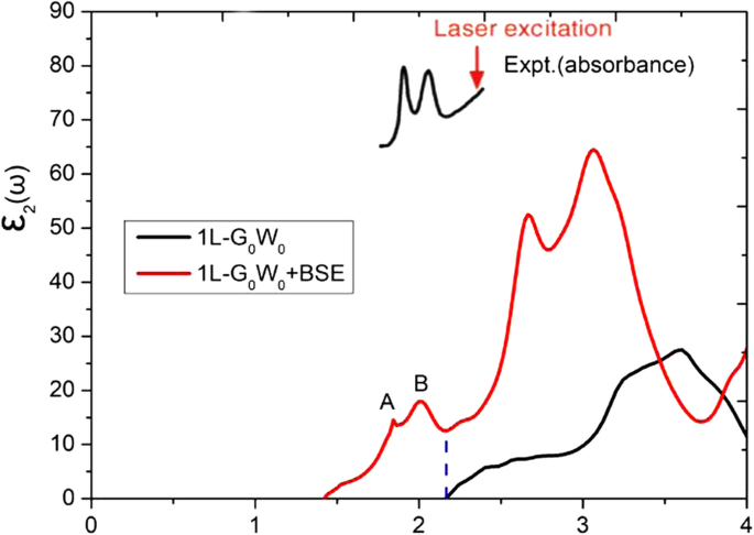
단층 MoS의 여기자 효과2 중요한 것으로 밝혀졌으며 광발광에 의해 관찰되었습니다. 준 입자 G0을 사용했습니다. 여0 방법 [38], 그리고 여기자 효과를 설명하기 위한 Bethe-Salpeter 방정식(BSE) [39, 40]. 단층 MoS2의 밴드 갭 k의 경우 2.32 및 2.27 eV로 계산됩니다. -15 × 15 × 1 및 24 × 24 × 1 Γ의 점 메쉬 -중심 그리드, G0에 의해 획득 여0 SOC 계산과 함께. 유전 함수의 허수 부분은 그림 1에 나와 있으며 G0 여0 및 G0 여0 + 광우병 방법. 1.84 및 1.99 eV에서 두 개의 엑시톤 피크가 발견되었으며 이는 실험적 관찰과 잘 일치합니다[4, 41]. 비록 G0 여0 +BSE 체계는 여기자 효과를 더 잘 설명할 수 있습니다. 이 백서에서는 GGA-PBE 기능에서 (여기자 피크가 없는) 결과만 제시합니다.
<그림>
단층 MoS2에 대한 유전 함수의 허수부 , G0을 사용하여 여0 및 G0 여0 +BSE 방법, 각각. MoS2에 대한 실험적 흡수 스펙트럼 Ref.에서 추출됩니다. [4]
결과 및 토론
MoS의 전자 구조2 다층
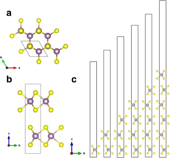
결정질 MoS2 자연적으로 발생하며 3가지 결정 유형이 있습니다. 1T , 2H , 및 3R , 각각 삼각형, 육각형 및 능면체 기본 단위 셀을 가진 결정에 해당합니다[9]. 2하 -MoS2 가장 안정적인 구조로 알려져 있습니다[10]. 따라서 2H만 고려합니다. 대량 MoS2 유형 이 작품에서. 대량 2H -MoS2 6개의 황 원자로 둘러싸인 몰리브덴 원자 층으로 구성된 육각형 층 구조를 가지고 있으며 S-Mo-S 시트가 반대로 쌓여 있습니다(그림 2 참조). 대량의 인접 시트 2H -MoS2 약한 반 데르 발스 상호 작용과 약하게 연결되어 있습니다. 단층 MoS2 그런 다음 대량에서 쉽게 각질을 제거할 수 있습니다. 벌크 MoS2의 격자 상수 a =b로 계산됩니다. =3.19Å, c =12.41 Å, 보고된 a =b 값과 일치 =3.18Å, c =13.83 Å [18]. 단층 MoS2에 최적화된 격자 상수 a =b입니다. =3.19 Å, 이는 대량 MoS2와 일치합니다. . a에서 계산된 격자 상수는 표 1과 같이 , b 방향은 MoS2의 다른 레이어 수에 대해 동일합니다. . Kumar et al.에 의해서도 보고되었습니다. [19] 격자 상수(a, b ) 단층 MoS2 벌크와 거의 동일합니다.
<그림>
아 상위 뷰 및 b 대량 MoS2의 측면도 . ㄷ MoS2의 단층, 이중층, 삼중층 및 4, 5, 6층 구조의 측면도 . 단위 셀은 b에 표시됩니다. . 보라색과 노란색 공은 각각 Mo 및 S 원자를 나타냅니다.
그림 3은 MoS2 레이어 수의 계산된 밴드 구조와 전자 밀도 상태(DOS)를 보여줍니다. . 단층, 이중층, 삼중층 및 4층 및 벌크 MoS2에 대한 결과 5층 및 6층 MoS2에 대한 결과는 그림 3에 나와 있습니다. 4층 및 벌크와 매우 유사합니다. 단층 MoS2용 , VBM(valence band maximum)과 CBM(conduction band minimum)은 모두 BZ의 K-point에 나타나며 1.64 eV의 직접적인 밴드갭을 나타낸다. 이중층 및 삼중층 MoS2용 , 두 VBM은 모두 Γ 지점에 위치하는 반면 두 CBM은 K 지점에 있으므로 각각 1.17 및 1.08 eV의 간접 간격이 발생합니다. 그러나 MoS2의 수로 레이어가 4개 이상으로 증가하면 모든 다중 레이어 MoS2 VBM이 Γ 지점에 위치하는 것과 동일한 문자를 표시하는 반면 CBM은 Γ와 K 지점 사이에 있으며 이는 벌크에서와 동일합니다. 간접 밴드 갭은 4, 5, 6층 MoS2의 경우 1.03eV, 1.01eV, 0.99eV, 0.93eV입니다. , 및 대량, 각각. PBE-D2 및 HSE06 계산(표 1) 모두 MoS2 층이 감소하는데, 이는 슬래브에 전자가 크게 가두어 있기 때문입니다[4, 5, 19, 42]. 또한 대량 MoS2 슬라브가 단일 레이어로 줄어들면 앞에서 언급한 것처럼 직접 밴드갭 반도체로 변합니다. 벌크 MoS2 간접 갭 반도체입니다. 그림 3a에서, 벌크 MoS2의 밴드 구조 플롯 밴드 분할 표시(단일층 MoS2의 분할과 비교) ), 주로 주변 -층간 결합으로 인한 점 [16]. 2층(2L) 및 2L 이상의 MoS2를 위한 밴드 구조 층간 결합으로 인해 유사한 밴드 분할을 나타냅니다. 그러나 대량의 밴드 분할은 다층 MoS2의 것보다 다소 중요합니다. , 다층보다 벌크에서 (약간) 더 강한 층간 결합을 나타냅니다. 반면, BZ에서 K 지점 부근의 밴드 분할은 매우 작습니다. 가장 높은 점유 대역에 대한 점 K의 전자 상태는 주로 d로 구성됩니다. xy 및 \( {d}_{x^2-{y}^2} \) Mo 원자의 궤도와 (p의 작은 부분) x , 피와 )-S 원자의 궤도(그림 4b 참조). Mo 원자는 S-Mo-S 시트의 중간 층에 위치하여 K 지점에서 무시할 수 있는 층간 결합을 유발합니다(MoS2 레이어는 S와 S)입니다. 도 4에 도시된 바와 같이, 가장 높은 점유 대역에 대한 점 Γ에서의 전자 상태는 \({d}_{z^2} \ ) Mo 원자의 궤도 및 pz S 원자의 궤도. 따라서 S-S 결합(층간 결합)은 점 K에서보다 점 Γ에서 분명히 더 강력합니다. 우리의 결과는 다른 이론적인 작업과 일치합니다[21]. 일반적으로 말하면, 소수층 MoS2 상태의 전자 밀도 대량 MoS2와 유사합니다. (그림 3 참조), 대량 MoS2 이후 실제로 MoS2 레이어.
<그림>
a 상태의 계산된 밴드 구조 및 밀도 단층(실선) 및 벌크(대시선), b 이중층, c 삼중층 및 d 4층 MoS2 . a에서 , 점 K에서 벌크 및 단층에 대한 가장 높은 점유 대역은 동일한 에너지로 설정됩니다. 벌크의 전도대 최소값은 B0 지점에 있습니다.
<그림>
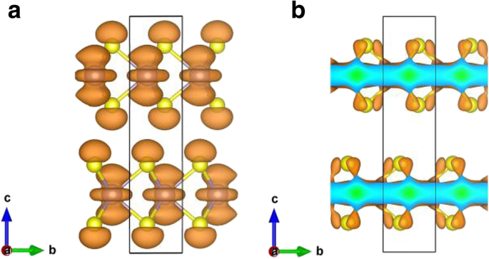
a에서 가장 높은 점유 대역의 전하 분포 가리키다 및 b 대량 MoS2의 경우 K 포인트 . 등가곡면 값은 0.004 e/Å
3
로 설정됩니다.
단층 MoS2의 결합 특성을 깊이 탐구하기 위해 , 변형 전하 밀도는 그림 5a에 나와 있습니다. 변형 전하 밀도는 Δρ로 지정됩니다. 1 (r ) =ρ (r ) − ∑μρ원자 (r − Rμ ) 여기서 ρ (r )는 총 전하 밀도이고 ∑μρ원자 (r − Ru )는 독립 원자 전하 밀도의 중첩을 나타냅니다. 결과는 MoS2 단층은 명확한 공유(Mo-S 원자 사이의 실선 윤곽선)와 강한 이온 상호작용(점선과 실선 윤곽의 교대 영역으로 표시됨)이 특징입니다. 단층 MoS2의 결합 강도를 보려면 벌크와 비교하여 단층과 벌크 MoS2 간의 전하 밀도 차이 , Δρ2 (r ), 그림 5b에도 나와 있습니다. 전하 밀도 차이는 Δρ로 정의됩니다. 2 (r ) =ρ1L (r ) − ρ대량 (r ), 여기서 ρ1L (r ) 및 ρ대량 (r )는 단층 및 벌크 MoS2의 총 전하 밀도입니다. , 각각. 그림 5b는 벌크의 경우보다 단층의 경우 더 강한 전자 결합을 나타내며, 이는 단층의 Mo-S 원자 사이의 더 큰 전하 축적(실선 등고선)과 더 강한 이온 결합에 의해 반영됩니다. 단층 MoS2 그림 5b에서 점선과 실선 윤곽이 교차하는 영역이 벌크 영역보다 더 중요하기 때문입니다. 또한, 전하 차이 플롯(그림 5b)은 단층의 Mo 원자가 벌크의 Mo 원자보다 더 많은 전자를 잃는 것을 나타냅니다. 따라서 단층의 이온성은 벌크보다 강합니다. 그러나 그림 5b에서 전하 차이의 크기 차수가 상당히 작다는 점을 지적해야 합니다(그림 5b의 등고선 간격은 2.5 × 10
-4
에 불과합니다). e/Å
3
). 다시 양자 구속 효과로 판단하면 단층의 층간 상호 작용은 벌크보다 강해야합니다. 따라서 단층의 밴드갭(1.64eV)은 벌크(0.93eV)보다 클 것으로 예상됩니다. Quantum confinement는 layer number가 증가함에 따라 감소하며[4, 42], interlayer coupling을 강화하고 intra-layer interaction을 감소시킵니다. 따라서 MoS2의 밴드갭은 층간 결합이 증가함에 따라 감소합니다. 이중층 MoS2에 대한 층간 전하 밀도 재분배 , Δρ3 (r ), 그림 5c에도 나와 있습니다. Δρ3 (r )는 Δρ로 지정됩니다. 3 (r ) =ρ2L (r ) − ρ레이어1 (r ) − ρ레이어2 (r ), 여기서 ρ2L (r ), ρ레이어1 (r ), ρ레이어2 (r )는 이중층 MoS2의 전하 밀도입니다. , 이중층 MoS2의 첫 번째 레이어 이중층 MoS2의 두 번째 레이어 , 각각. 이중층 MoS2의 layer1 및 layer2의 전하 밀도 이중층 MoS2의 해당 구조를 사용하여 계산됩니다. . MoS2에서 요금 이전 MoS2 사이의 중간 영역에 레이어(이중층) 레이어는 실선으로 표시된 그림 5c에서 명확하게 볼 수 있습니다. 이중층 MoS2에서 원자층 간의 이온 상호작용 점선과 실선 윤곽이 교차하는 영역에서도 볼 수 있듯이 명확합니다. 다시, 층간 전하 밀도의 크기, Δρ3 (r ), 매우 작습니다(등고선 간격은 2.5 × 10
-4
에 불과함). e/Å
3
). 일반적으로 2L, 3L, ..., 벌크 MoS2의 층간 전하 밀도 재분배 시스템은 모두 매우 유사합니다.
<그림>
아 변형 전하 밀도, Δρ1 (r ) =ρ (r ) − ∑μρ원자 (r − Rμ ), 단층 MoS2에서 . ㄴ 단층의 전하 밀도와 벌크의 해당 층 간의 차이. ㄷ 이중층 MoS2의 층간 전하 밀도 재분배 . a 등고선 간격 2.5 × 10
−2
입니다. e/Å
3
, b 및 c 2.5 × 10
−4
입니다. e/Å
3
. 주황색 실선과 파란색 파선은 Δρ에 해당합니다.> 0 및 Δρ <0, 각각
MoS의 광학적 속성2 다층
재료의 기저 상태 전자 구조가 얻어지면 광학 특성을 조사할 수 있습니다. 유전 함수 \( {\varepsilon}_2^{\alpha \beta}\left(\omega \right) \)의 허수 부분은 다음 방정식 [43]에 의해 결정됩니다.
여기서 인덱스 α 및 β 직교 방향을 나타냅니다. c 및 v 전도대 및 가전자대 참조, E크크 및 Evk 는 각각 전도대와 가전자대의 에너지입니다. Kramers-Kronig 역전은 허수부에 의해 결정되는 유전 함수 \( {\varepsilon}_1^{\alpha \beta}\left(\omega \right) \) 바렙실론}_2^{\alpha \beta}\left(\omega \right) \):
행렬 요소 \( \left\langle {u}_{ck+{e}_{\alpha }q}|{u}_{vk}\right\rangle \)가 k -벡터, 항 \( \left\langle {u}_{ck+{e}_{\alpha }q}|{u}_{vk}\right\rangle \left\langle {u}_{ck+{ e}_{\beta }q}|{u}_{vk}\right\rangle \ast \) Eq. (1) 합계를 벗어날 수 있습니다. 식에서 (1) \( {\varepsilon}_2^{\alpha \beta}\left(\omega \right) \) 에서 대부분의 분산은 델타 함수 δ에 대한 합으로 인한 것입니다. (이크크 − Evk − ℏω ). 이 합계는 JDOS(Joint Density of State)를 정의하여 에너지에 대한 통합으로 변환될 수 있습니다. [25, 44],
ℏω 같음 E크크 − Evk , SㅋE로 표시되는 일정한 에너지 표면을 나타냅니다. 크크 − Evk =ℏω =상수. 상태 J의 결합 밀도 이력서 (ω )는 가전자대에서 전도대로의 전이 및 J의 큰 피크와 관련이 있습니다. 이력서 (ω ) ∇k 스펙트럼에서 시작됩니다. (이크크 − Evk ) ≈ 0. k의 포인트 -공백 여기서 ∇k (이크크 − Evk ) =0은 임계점 또는 반 호브 특이점(VHS)이라고 하며 E크크 − Evk 임계점 에너지[26, 27]라고 합니다. 임계점 ∇k이크크 =∇k이vk =0은 일반적으로 높은 대칭 지점에서만 발생하는 반면 임계 지점 ∇k이크크 =∇k이vk ≠ 0은 Brillouin 구역의 모든 일반 지점에서 발생할 수 있습니다[27, 45]. 2차원의 경우 세 가지 유형의 임계점이 있습니다. 즉, P0 (최소 포인트), P1 (안장점) 및 P2 (최대 포인트). 포인트 P에서 0 또는 피2 , JDOS에서는 단계 함수 특이점이 발생했지만 안장점 P에서는 1 , JDOS는 로그 특이점[27]으로 설명됩니다. 더 자세하게, Eㄷ (카x , k와 ) − Ev (카x , k와 )는 임계점에 대해 Taylor 급수에서 확장될 수 있습니다. 확장을 2차 항으로 제한하고 선형 항은 특이점의 속성으로 인해 발생하지 않으므로 다음을 얻습니다.
따라서 세 가지 유형의 임계점이 나타납니다. P의 경우 0 , (bx> 0, b와> 0), P1 , (bx> 0, b와 <0) 또는 (bx <0, b와> 0) 및 P의 경우 2 , (bx <0, b와 <0). 이 논문에서는 MoS2의 경우 다중 레이어, P만 0 임계점이 관련되어 있습니다.
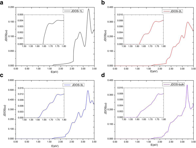
그림 6a는 MoS2의 유전 함수 \( {\varepsilon}_2^{xx}\left(\omega \right) \)의 허수 부분을 보여줍니다. E용 다중 레이어 ||x. 우리는 유전 함수 \( {\varepsilon}_2^{xx}\left(\omega \right) \) 의 허수 부분이 안정기를 가지고 있고 MoS2 1.75 eV~2.19 eV 범위에서 거의 동일합니다. 임계값 에너지에서 최대 1.75 eV까지, \( {\varepsilon}_2^{xx}\left(\omega \right) \)는 MoS2의 여러 다층에 대해 상당히 다릅니다. . 서로 다른 층에 있는 고원의 임계값과 끝 에너지는 다르며, 특히 단층의 \( {\varepsilon}_2^{xx}\left(\omega \right) \) 고원의 에너지 범위는 그것들보다 훨씬 더 넓습니다. 다른 다층의. 단층 MoS2의 임계 에너지 유전 기능은 1.64eV의 직접 밴드갭과 같습니다. 그러나 이중층 유전 함수의 임계 에너지는 1.17 eV의 간접 밴드갭이 아니라 가전자대와 전도대 사이의 최소 직접 에너지 갭인 1.62 eV이다. 직접적인 광전이로 분류되는 전자파 벡터가 동일한 가전자대와 전도대 사이의 전이만을 연구하기 때문이다[36, 47]. MoS2의 수로 레이어가 4로 증가하면 다층 MoS2의 \( {\varepsilon}_2^{xx}\left(\omega \right) \) 시스템은 벌크와 거의 구별할 수 없었습니다. 따라서 여기에서는 단층, 이중층 및 삼중층의 고원과 벌크 MoS2에 대해서만 자세히 논의합니다. . \( {\varepsilon}_2^{xx}\left(\omega \right) \) 단층, 이중층, 삼중층 및 벌크 MoS2 고원 각각 2.57eV, 2.28eV, 2.21eV 및 2.19eV에서 종료되었습니다. 이를 보다 정확하게 설명하기 위해 monolayer, bilayer, trilayer 및 bulk MoS의 JDOS2 그림 7에서 볼 수 있듯이 고원도 JDOS에 있는 것으로 나타납니다. 단층, 이중층 및 삼중층 JDOS의 고원은 각각 2.57 eV, 2.28 eV, 2.21 eV에서 종료되었으며, 이는 \( {\varepsilon}_2^{xx}\left(\omega \right ) \). 대량 MoS2의 경우 , JDOS의 고원은 2.09 eV에서 끝났으며 이는 유전 함수 \( {\varepsilon}_2^{xx}\left(\omega \right) \)에서 2.19 eV보다 약간 작습니다.
<그림>
아 유전 함수의 허수부, b 유전 함수의 실수부, c 흡수 계수 및 d 다른 수의 MoS2에 대한 반사 스펙트럼 레이어. c의 삽입 실험 데이터도 보여줍니다[46]
<그림>
단층, 이중층, 삼중층 및 벌크 MoS2에 대한 접합 상태 밀도
전자 전이를 정확하게 분석하고 유전 함수 \( {\varepsilon}_2^{xx}\left(\omega \right) \)에 대한 자세한 분석을 위해 직접 에너지 갭 ΔE(NC − NV), 단층, 이중층, 삼중층 및 벌크 MoS2의 전도대 및 가전자대 그림 8에 나와 있습니다. NC와 NV는 전도대와 가전자대의 서수를 나타냅니다. 따라서 NC =1, 2 및 3은 가장 낮은 재료, 두 번째로 낮은, 세 번째로 낮은 비어 있는 재료 밴드를 나타냅니다. 반면, NV =9, 18 및 27(단위 셀의 전자 수에 따라 다름)은 단층, 이중층 및 삼중층 MoS2의 가장 높은 점유 밴드를 나타냅니다. , 각각. 단층의 경우 0 ~ 2.57 eV 영역에서 전자 전이는 가장 높은 점유 대역 NV =9에서 가장 낮은 비점유 대역 NC =1로만 기여하는 것으로 나타났습니다. 그림 8a에서 최소값은 높은 대칭점에서 나타납니다. K 및 JDOS의 임계값(그림 7a)은 실제로 단층 MoS2의 직접적인 밴드갭인 1.64 eV에서 나타납니다. . 높은 대칭점 K 부근에서 ΔE(NC =1 − NV =9)의 곡선은 단층 MoS2에 대한 포물선과 유사합니다. . 따라서 ∇k (이크크 − Evk ) =0 at K point, 이는 높은 대칭점 K에서의 임계점을 의미한다. 2차원 구조에서 이 임계점은 P에 속한다. 0 유형 특이점 [27], 따라서 JDOS의 한 단계로 이어집니다. 따라서 JDOS 고원의 임계 에너지는 임계점 에너지 1.64 eV에서 발견됩니다. JDOS 고원의 끝 에너지는 2.57 eV에 가깝고, 이는 두 개의 P0 점 B1에서 특이점 입력(k =(0.00, 0.16, 0.00)) 및 점 B2(k =(− 0.10, 0.20, 0.00)). 두 임계점 B1과 B2 근처의 ΔE(NC =1 − NV =9) 곡선의 기울기는 매우 작아서 JDOS가 급격히 증가합니다(Eq.(5) 참조). JDOS의 긴 고원에 대한 주요 임계점은 유형, 위치, 전이 대역 및 직접 에너지 갭 ΔE(NC − NV)를 포함하여 표 2에 나열되어 있습니다. 또한 ∇k이크크 =∇k이vk =0은 가전자대와 전도대의 기울기가 수평인 높은 대칭점 K에서 발생했습니다. 동안 ∇k이크크 =∇k이vk ≠ 0은 점 B1과 B2에서 발생했는데, 이는 두 띠의 기울기가 평행함을 의미합니다. 동시에, 단일층에 대한 밴드 구조 및 직접 에너지 갭에 대한 분석(그림 8a 참조)은 직접 에너지 갭 ΔE가 2.65eV 미만일 때 NV =9와 NC =1 사이의 전이만이 JDOS에 기여한다는 것을 보여줍니다. ΔE가 2.65 eV보다 크면 NV =9에서 NC =2로의 전환도 JDOS에 기여하기 시작합니다. ΔE가 2.86eV 이상에 도달하면 NV =9에서 NC =3으로의 전환이 JDOS에 영향을 미칩니다. 2.65 eV보다 큰 에너지의 경우 그림 8a의 많은 대역이 JDOS에 기여할 것이라는 점을 지적해야 합니다. 단층 MoS2의 JDOS 1.64 ~ 2.57 eV 범위에서 안정기를 나타내며 |Mvc 식의 변형 |
2
/ω
2
이 범위에서 작은 것으로 나타났습니다. 식에 따르면 (1) and (5), the imaginary part of the dielectric function \( {\varepsilon}_2^{xx}\left(\omega \right) \) is mainly decided by the JDOS and the transition matrix elements, this gives a similar plateau for the imaginary part of dielectric function \( {\varepsilon}_2^{xx}\left(\omega \right) \) as compared to JDOS.
Direct energy gaps, ΔE(NC − NV), between conduction and valence bands for the a monolayer, b bilayer, c trilayer, and d bulk MoS2 . 아 –d There are three, six, twelve, and six critical points in interband transitions for the monolayer, bilayer, trilayer, and bulk MoS2 , 각각
For bilayer MoS2 , in the region of 0 ~ 2.28 eV (the endpoint of JDOS plateau), the electronic transitions are contributed to NV =17, 18 to NC =1, 2. The minimum energy in ΔE(NC − NV) is situated at the K point with a gap of 1.62 eV. In Fig. 8b, similar to monolayer MoS2 , bilayer MoS2 holds two parabolic curves going upward (which come from ΔE(NC = 1 − NV = 18) and ΔE(NC = 2 − NV = 18)) at K point. Therefore, there are two P0 type singularities (∇k (이ck − Evk ) = 0) at K point, causing a step in the JDOS. The critical point energies are both 1.62 eV, this is because that the conduction bands (NC =1 and NC =2) are degenerate at point K (as shown in Fig. 3b), which results in the same direct energy gap between transitions of NV =18 to NC =1 and NV =18 to NC =2. From Fig. 8b, as the direct energy gap is increased to 1.69 eV, two new parabolas (which come from ΔE(NC = 1 − NV = 17) and ΔE(NC = 2 − NV = 17)) appear and two new singularities emerge again at K point in the direct energy gap graph, leading to a new step in JDOS for bilayer MoS2 (see Fig. 7b). As a result, the JDOS of the bilayer MoS2 has two steps around the threshold of long plateau (see inset in Fig. 7b). Two parabolas (in Fig. 8b) contribute to the first step and four parabolas contribute to the second step in JDOS. It means that the value of the second step is roughly the double of the first one. As the ΔE reaches to 2.28eV, two new singularities appear at Γ point (where interband transitions come from Γ(NV =18→NC =1) and Γ(NV =18→NC =2)), which have great contribution to the JDOS and bring the end to the plateau. Our calculations demonstrate that ∇k이ck = ∇k이vk = 0 are satisfied not only at high symmetry point K, but also at high symmetry point Γ. Similar to the case of monolayer, we found that the term of |Mvc |
2
/ω
2
is a slowly varying function in the energy range of bilayer JDOS plateau; hence, \( {\varepsilon}_2^{xx}\left(\omega \right) \) of bilayer have a similar plateau in the energy range.
For trilayer MoS2 , in the region of 0 ~ 2.21 eV, the JDOS are contributed from electronic transitions of NV =25, 26, and 27 to NC =1, 2, and 3. As shown in Fig. 8c, trilayer MoS2 have nine singularities at three different energies (ΔE =1.61 eV, 1.66 eV, and 1.72 eV, respectively) at the K point. Figure 3c depicts that the conduction bands (NC =1, 2, 3) are three-hold degenerate at point K; this means that there are three singularities at each critical point energy. According to our previous analysis, the JDOS and \( {\varepsilon}_2^{xx}\left(\omega \right) \) of trilayer MoS2 will show three steps near the thresholds of the long plateaus, the endpoints of the long plateaus of trilayer JDOS, and \( {\varepsilon}_2^{xx}\left(\omega \right) \) are then owing to the appearance of three singularities at Γ point with ΔE =2.21 eV (see Fig. 7c), which come from the interband transitions of Γ(NV =27→NC =1, 2, 3).
For bulk MoS2 , the thresholds of \( {\varepsilon}_2^{xx}\left(\omega \right) \) and JDOS are also located at K point, with the smallest ΔE(NC − NV) equals to 1.59 eV. Nevertheless, there is no obvious step appeared in the thresholds of plateaus for both the \( {\varepsilon}_2^{xx}\left(\omega \right) \) and JDOS (see Fig. 6a and Fig. 7d). Based on the previous analysis, the number of steps in the monolayer, bilayer, and trilayer MoS2 are 1, 2, and 3, respectively. As the number of MoS2 layers increases, the number of steps also increases in the vicinity of the threshold energy. Thus, in the bulk MoS2 , the JDOS curve is composed of numerous small steps around the threshold energy of the long plateau, and finally the small steps disappear near the threshold energy since the width of the small steps decreases. In the region of 0 ~ 2.09 eV, the electron transitions of bulk MoS2 are contributed to NV =17, 18 to NC =1, 2. The 2.09 eV is the endpoint of JDOS plateau of bulk MoS2 , which is attributed to two singularities, i.e., the interband transitions of Γ(NV =18→NC =1) as well as Γ(NV =18→NC =2), as presented in Fig. 8d. However, the plateau endpoint of the imaginary part of dielectric function \( {\varepsilon}_2^{xx}\left(\omega \right) \) is 2.19 eV, which is greater than the counterpart of JDOS (e.g., 2.09 eV). Checked the transition matrix elements, it verified that some transitions are forbidden by the selection rule in the range of 2.09 eV to 2.19 eV. Therefore, the imaginary part of the dielectric function \( {\varepsilon}_2^{xx}\left(\omega \right) \) is nearly invariable in the range of 2.09 ~ 2.19 eV. As a result, the plateau of \( {\varepsilon}_2^{xx}\left(\omega \right) \) of bulk MoS2 is then 1.59 ~ 2.19 eV.
It has been shown that these thresholds of the JDOS plateaus are determined by singularities at the K point for all of the studied materials, see Fig. 8. The endpoint energy of the monolayer JDOS plateau is determined by two critical points at B1 and B2 (Fig. 8a). Nevertheless, the endpoint energies of bilayer, trilayer, and bulk JDOS plateaus are all dependent on the critical points at Γ(Fig. 8b–d). The interlayer coupling near point Γ is significantly larger than the near point K for all the systems of multilayer MoS2 . The smallest direct energy gap decreases and the interlayer coupling increases as the number of layers grow. With the layer number increases, a very small decrease of direct energy gap at point K and a more significant decrease of direct energy gap at point Γ can be observed, as a result, a faint red shift in the threshold energy and a bright red shift in the end of both JDOS and \( {\varepsilon}_2^{xx}\left(\omega \right) \) plateaus can also be found. For monolayer MoS2 , the smallest ΔE(NC − NV) at point Γ is 2.75 eV which is larger than that at point B1 (or point B2) with a value around 2.57 eV. When it goes to multilayer and bulk MoS2 , the strong interlayer coupling near point Γ makes the smallest ΔE(NC − NV) at Γ less than those at point B1 (or point B2). Hence, monolayer owns the longest plateau of JDOS, which is between 1.64 eV and 2.57 eV. The shortest plateau of JDOS (from 1.59 eV to 2.09 eV) is shown in the bulk.
As the energy is increased to the value larger than the endpoint of long platform of the dielectric function, a peak A can be found at the position around 2.8 eV, for almost all the studied materials (Fig. 6a). The width of peak A for monolayer is narrower compared with those of multilayer MoS2; however, the intensity of peak A for monolayer is found to be a little stronger than multilayers. The differences between the imaginary parts of dielectric function for the monolayer and multilayer MoS2 are evident, on the other hand, the differences are small for multilayer MoS2 .
In order to explore the detailed optical spectra of MoS2 multilayers, the real parts of the dielectric function ε1 (ω ), the absorption coefficients α (ω ), and the reflectivity spectra R (ω ) are presented in Fig. 6b–d. Our calculated data of bulk MoS2 for the real and imaginary parts of the dielectric function, ε1 (ω ) and ε2 (ω ), the absorption coefficient α (ω ) and the reflectivity R (ω ) agree well with the experimental data, except for the excitonic features near the band edge [48,49,50]. The calculated values of , which is called the static dielectric constant, for MoS2 multilayers and bulk can be found in Table 1. From Table 1, the calculated values of \( {\varepsilon}_1^{xx}(0) \) for multilayers and bulk MoS2 are all around 15.5, which is very close to the experimental value of 15.0 for bulk MoS2 [50]. The values of \( {\varepsilon}_1^{xx}(0) \) increase with the increasing number of MoS2 layers. For monolayer MoS2 , a clear peak B of \( {\varepsilon}_1^{xx}\left(\omega \right) \) appears about 2.54 eV. Peak B of monolayer is clearly more significant than multilayers, and they are all similar for multilayer MoS2 . As the layer number increases, the sharp structures (peak B) also move left slightly. In Fig. 6c, we also observe the emergence of long plateaus in the absorption coefficients, and absorption coefficients are around 1.5 × 10
5
cm
−1
at the long plateaus. There are also small steps around the thresholds for the absorption coefficients, which are consistent to those of the imaginary parts of dielectric function. With the layer number increases, the threshold energy of absorption coefficient decreases, while the number of small steps increases at the starting point of the plateau. For monolayer and multilayer MoS2 , strong absorption peaks emerge at visible light range (1.65–3.26 eV), and the monolayer MoS2 own a highest absorption coefficient of 1.3 × 10
6
cm
−1
. The theoretical absorption coefficients for different number of MoS2 layers are compared with confocal absorption spectral imaging of MoS2 (the inset) [46], as shown in Fig. 6c. For monolayer and multilayer MoS2 , a large peak of α (ω ) can be found at the position around 2.8 eV for both the calculation and experiment [46, 51]. Furthermore, a smoothly increase of α (ω ) can be found between 2.2 and 2.8 eV for both the theoretical and experimental curves. Therefore, from Fig. 6c, the calculated absorption coefficients of MoS2 multilayers show fairly good agreement with the experimental data [46], except for the excitonic peaks. The reflectivity spectra are given in Fig. 6d. The reflectivity spectra of MoS2 multilayers are all about 0.35–0.36 when energy is zero, which means that MoS2 system can reflect about 35 to 36% of the incident light. In the region of visible light, the maximum reflectivity of monolayer MoS2 is 64%, while the maxima of multilayer and bulk MoS2 are all about 58%. Because of the behaviors discussed, MoS2 monolayer and multilayers are being considered for photovoltaic applications.
결론
In this study, by employing ab initio calculations, the electronic and optical properties of MoS2 multilayers are investigated. Compared to bulk MoS2 , the covalency and ionicity of monolayer MoS2 are found to be stronger, which results from larger quantum confinement in the monolayer. With the increase of the layer number, quantum confinement and intra-layer interaction both decrease, meanwhile, the interlayer coupling increases, which result in the decrease of the band gap and the minimum direct energy gap. As the layer number becomes larger than two, the optical and electronic properties of MoS2 multilayers start to exhibit those of bulk. Band structures of multilayers and bulk show splitting of bands mainly around the Γ-point; however, splitting of bands in the vicinity of K point are tiny, owing to the small interlayer coupling at point K.
For optical properties, Van Hove singularities lead to the occurrence of long plateaus in both JDOS and \( {\varepsilon}_2^{xx}\left(\omega \right) \). At the beginnings of these long plateaus, monolayer, bilayer, and trilayer structures appear one, two, and three small steps, respectively. With the layer number increases, the number of small steps increases and the width of the small steps decreases, leading to unobvious steps. A small red shift in the threshold energy and a noticeable red shift in the end of both JDOS and \( {\varepsilon}_2^{xx}\left(\omega \right) \) plateaus are observed, since the increased number of layers leads to small changes in the direct energy gap near point K (weak interlayer coupling) and larger changes near point Γ (stronger interlayer coupling). Thus, the longest plateau and shortest plateau of JDOS are from the monolayer and bulk, respectively. Our results demonstrate that the differences between electronic and optical properties for monolayer and multilayer MoS2 are significant; however, the differences are not obvious between the multilayer MoS2 . The present data can help understand the properties of different layers of MoS2 , which should be important for developing optoelectronic devices.


 -층간 결합으로 인한 점 [16]. 2층(2L) 및 2L 이상의 MoS2를 위한 밴드 구조 층간 결합으로 인해 유사한 밴드 분할을 나타냅니다. 그러나 대량의 밴드 분할은 다층 MoS2의 것보다 다소 중요합니다. , 다층보다 벌크에서 (약간) 더 강한 층간 결합을 나타냅니다. 반면, BZ에서 K 지점 부근의 밴드 분할은 매우 작습니다. 가장 높은 점유 대역에 대한 점 K의 전자 상태는 주로 d로 구성됩니다. xy 및 \( {d}_{x^2-{y}^2} \) Mo 원자의 궤도와 (p의 작은 부분) x , 피 와 )-S 원자의 궤도(그림 4b 참조). Mo 원자는 S-Mo-S 시트의 중간 층에 위치하여 K 지점에서 무시할 수 있는 층간 결합을 유발합니다(MoS2 레이어는 S와 S)입니다. 도 4에 도시된 바와 같이, 가장 높은 점유 대역에 대한 점 Γ에서의 전자 상태는 \({d}_{z^2} \ ) Mo 원자의 궤도 및 p z S 원자의 궤도. 따라서 S-S 결합(층간 결합)은 점 K에서보다 점 Γ에서 분명히 더 강력합니다. 우리의 결과는 다른 이론적인 작업과 일치합니다[21]. 일반적으로 말하면, 소수층 MoS2 상태의 전자 밀도 대량 MoS2와 유사합니다. (그림 3 참조), 대량 MoS2 이후 실제로 MoS2 레이어.
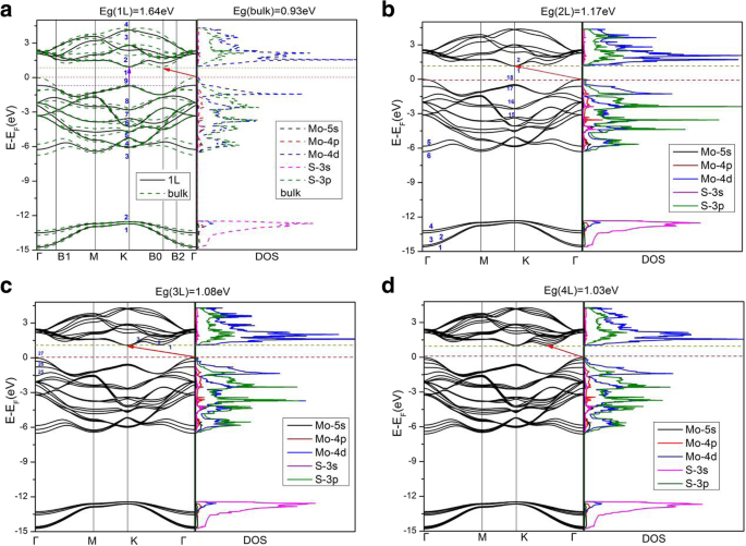
 및 b 대량 MoS2의 경우 K 포인트 . 등가곡면 값은 0.004 e/Å
3
로 설정됩니다.
및 b 대량 MoS2의 경우 K 포인트 . 등가곡면 값은 0.004 e/Å
3
로 설정됩니다. 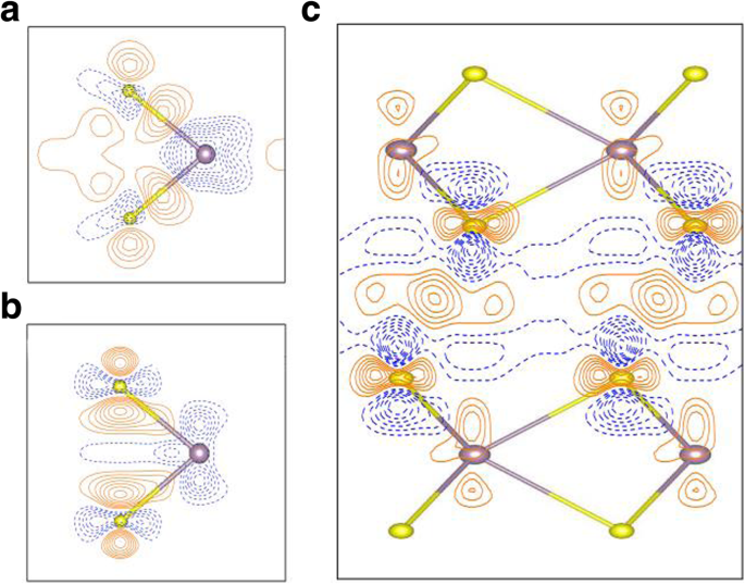
 입니다. 언급된 매개변수 방정식은 다음과 같습니다.
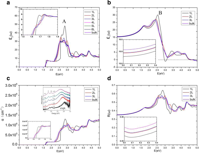

 , which is called the static dielectric constant, for MoS2 multilayers and bulk can be found in Table 1. From Table 1, the calculated values of \( {\varepsilon}_1^{xx}(0) \) for multilayers and bulk MoS2 are all around 15.5, which is very close to the experimental value of 15.0 for bulk MoS2 [50]. The values of \( {\varepsilon}_1^{xx}(0) \) increase with the increasing number of MoS2 layers. For monolayer MoS2 , a clear peak B of \( {\varepsilon}_1^{xx}\left(\omega \right) \) appears about 2.54 eV. Peak B of monolayer is clearly more significant than multilayers, and they are all similar for multilayer MoS2 . As the layer number increases, the sharp structures (peak B) also move left slightly. In Fig. 6c, we also observe the emergence of long plateaus in the absorption coefficients, and absorption coefficients are around 1.5 × 10
5
cm
−1
at the long plateaus. There are also small steps around the thresholds for the absorption coefficients, which are consistent to those of the imaginary parts of dielectric function. With the layer number increases, the threshold energy of absorption coefficient decreases, while the number of small steps increases at the starting point of the plateau. For monolayer and multilayer MoS2 , strong absorption peaks emerge at visible light range (1.65–3.26 eV), and the monolayer MoS2 own a highest absorption coefficient of 1.3 × 10
6
cm
−1
. The theoretical absorption coefficients for different number of MoS2 layers are compared with confocal absorption spectral imaging of MoS2 (the inset) [46], as shown in Fig. 6c. For monolayer and multilayer MoS2 , a large peak of α (ω ) can be found at the position around 2.8 eV for both the calculation and experiment [46, 51]. Furthermore, a smoothly increase of α (ω ) can be found between 2.2 and 2.8 eV for both the theoretical and experimental curves. Therefore, from Fig. 6c, the calculated absorption coefficients of MoS2 multilayers show fairly good agreement with the experimental data [46], except for the excitonic peaks. The reflectivity spectra are given in Fig. 6d. The reflectivity spectra of MoS2 multilayers are all about 0.35–0.36 when energy is zero, which means that MoS2 system can reflect about 35 to 36% of the incident light. In the region of visible light, the maximum reflectivity of monolayer MoS2 is 64%, while the maxima of multilayer and bulk MoS2 are all about 58%. Because of the behaviors discussed, MoS2 monolayer and multilayers are being considered for photovoltaic applications.
, which is called the static dielectric constant, for MoS2 multilayers and bulk can be found in Table 1. From Table 1, the calculated values of \( {\varepsilon}_1^{xx}(0) \) for multilayers and bulk MoS2 are all around 15.5, which is very close to the experimental value of 15.0 for bulk MoS2 [50]. The values of \( {\varepsilon}_1^{xx}(0) \) increase with the increasing number of MoS2 layers. For monolayer MoS2 , a clear peak B of \( {\varepsilon}_1^{xx}\left(\omega \right) \) appears about 2.54 eV. Peak B of monolayer is clearly more significant than multilayers, and they are all similar for multilayer MoS2 . As the layer number increases, the sharp structures (peak B) also move left slightly. In Fig. 6c, we also observe the emergence of long plateaus in the absorption coefficients, and absorption coefficients are around 1.5 × 10
5
cm
−1
at the long plateaus. There are also small steps around the thresholds for the absorption coefficients, which are consistent to those of the imaginary parts of dielectric function. With the layer number increases, the threshold energy of absorption coefficient decreases, while the number of small steps increases at the starting point of the plateau. For monolayer and multilayer MoS2 , strong absorption peaks emerge at visible light range (1.65–3.26 eV), and the monolayer MoS2 own a highest absorption coefficient of 1.3 × 10
6
cm
−1
. The theoretical absorption coefficients for different number of MoS2 layers are compared with confocal absorption spectral imaging of MoS2 (the inset) [46], as shown in Fig. 6c. For monolayer and multilayer MoS2 , a large peak of α (ω ) can be found at the position around 2.8 eV for both the calculation and experiment [46, 51]. Furthermore, a smoothly increase of α (ω ) can be found between 2.2 and 2.8 eV for both the theoretical and experimental curves. Therefore, from Fig. 6c, the calculated absorption coefficients of MoS2 multilayers show fairly good agreement with the experimental data [46], except for the excitonic peaks. The reflectivity spectra are given in Fig. 6d. The reflectivity spectra of MoS2 multilayers are all about 0.35–0.36 when energy is zero, which means that MoS2 system can reflect about 35 to 36% of the incident light. In the region of visible light, the maximum reflectivity of monolayer MoS2 is 64%, while the maxima of multilayer and bulk MoS2 are all about 58%. Because of the behaviors discussed, MoS2 monolayer and multilayers are being considered for photovoltaic applications.