

나노물질

산업 제조
그래핀 너머의 2차원(2D) 반도체는 가장 얇고 안정적인 알려진 나노물질을 나타냅니다. 21세기의 지난 10년 동안 제품군과 애플리케이션의 급속한 성장은 첨단 나노 및 광전자 기술에 전례 없는 기회를 가져왔습니다. 이 기사에서는 개발된 2D 나노 물질에 대한 최신 연구 결과를 검토합니다. 이러한 2차원 나노물질 및 이종구조의 고급 합성 기술을 요약하고 새로운 응용에 대해 논의했습니다. 제작 기술에는 최신 2D 반도체의 화학 기상 증착(CVD), 원자층 증착(ALD)에 특히 중점을 두고 비정질 및 결정질 2D 나노물질을 모두 제조하기 위한 기상 기반 증착 방법 및 새로운 반 데르 발스(vdW) 박리 접근법 개발 액체 금속의 2D 표면 산화막의 vdW 박리뿐 아니라 이종 구조에 대한 연구
그래핀의 고귀한 가격(2010)과 그래핀을 넘어선 2D 반도체 개발의 후속 발전에 이어, 21세기의 두 번째 10년 동안 2D 나노 물질 및 이의 이종 구조를 기반으로 하는 재료 과학의 독립적인 과학 분야의 실질적인 성장이 목격되었습니다. 세기 [1,2,3,4]. 보고된 2D 나노물질의 구조에서 전자 전달 및 밴드갭 변조로 인한 매우 흥미로운 물리화학적 현상이 관찰되었습니다[5, 6]. 그래핀은 밴드갭이 없기 때문에 반도체 특성을 나타내지 못하며 많은 관심을 받고 있으며, 전이금속 이칼코게나이드(TMDC), 육방정계 질화붕소(h) 등 그래핀과 유사한 다른 2차원 나노물질 개발에 많은 노력을 기울였다.> -BN), 블랙 포스펜 및 전이 금속 산화물 등 [7,8,9,10,11,12,13,14,15,16]. 그래핀을 넘어선 이 2D 나노물질 제품군은 금속에서 반금속, 그리고 반도체에서 절연체에 이르기까지 광범위한 특성을 포괄하는 광범위한 전자 특성을 나타냅니다[17,18,19,20]. 광범위한 전자 특성 외에도 2D 재료의 고표면적, 댕글링 본드 부족, 표면 상태의 특성, 고유한 스핀-궤도 결합 특성 및 양자 스핀 홀 효과를 비롯한 2D 재료의 다른 특성은 매우 흥미로운 특성을 조화시킵니다. 개별 나노구조 2D 재료 [21,22,23,24,25]. 결과적으로 이러한 유형의 2D 나노물질에 대한 과학계의 관심은 전례 없는 반도체 특성으로 인해 특히 지난 10년 동안 기하급수적으로 증가했습니다. 결과적으로, 이러한 관심은 그림 1에 제시된 2D 반도체(Web of Knowledge™ 데이터베이스)에 관한 출판된 기사의 비례적 기하급수적 증가에 의해 적절하게 반영되었습니다.
<사진>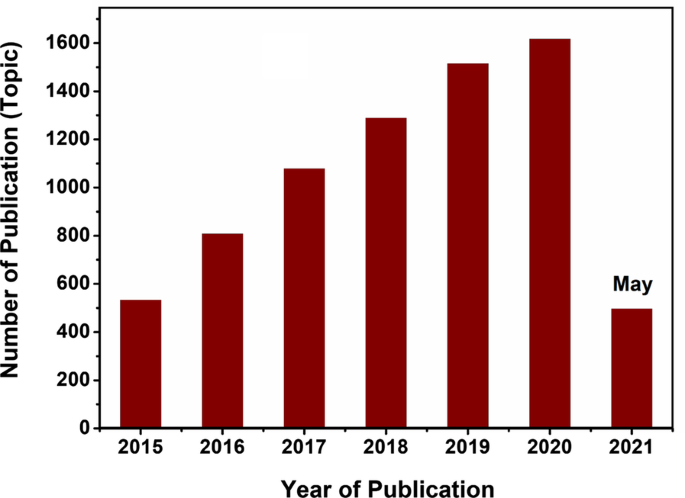
"2D 반도체에 대한 출판 기사 수의 역학 ” Web of Knowledge™ 기반
2D 반도체 나노물질의 특성에 대한 초기 측정은 고유한 전자 특성을 나타내었으며, 이는 미세 구조 및 벌크 대응물의 특성과 비교할 수 없었습니다. 이러한 구별되는 특징은 2D 물질의 나노 스케일 저차원성에서 비롯된 양자 구속 효과와 관련이 있습니다[26]. 따라서 이러한 2D 재료의 고유한 사양은 기본 물리학 및 화학을 연구할 수 있는 우수한 플랫폼을 제공합니다. 처음으로 광범위하게 조사된 2D 나노물질 부류는 층상 TMDC(XY 2 , 여기서 X =Mo, Ti, W 및 Y =S, Se 및 Te) [27,28,29,30,31,32,33,34,35,36,37,38,39]. 이 단계에서 얻은 결과는 디칼코게나이드 반도체가 2D 및 벌크 전도도(σ 1 /σ 2 ~ 10 2 –10 3 ) [40]. 또한 이황화 몰리브덴(MoS2 ), 직접 밴드갭 반도체[41]. 2D TMDC의 획득된 전자 특성은 차세대 나노 및 광전자 장치의 추가 개발에 중요한 의미를 갖습니다. 이러한 발견과 기타 등방성은 강한 중간층 X의 존재에서 발생합니다. –예 본딩은 레이어 간의 약한 vdW 상호 작용과 대조됩니다[42]. 예:TiS2 육각형 층 구조로 결정화되며, 여기서 Ti 원자의 육각형으로 채워진 시트 하나가 각 단층에 대해 두 개의 육각형 황 시트 사이에 끼어 있습니다[43]. 원자의 이 특정한 층상 구성은 층상 2D 나노구조의 vdW 박리를 가능하게 했습니다. 결과적으로, 초기 보고서의 대부분은 기계적 및 vdW 박리 기술에 의해 합성된 2D 재료의 특성에 중점을 두었습니다. 2D 필름의 초박형 특성으로 인해 투명하고 가볍고 유연하며 매우 흥미로운 특성을 가질 수 있습니다. 이러한 고유한 기능은 배터리, 슈퍼 커패시터 및 연료 전지와 같은 에너지 저장 및 변환 응용 분야와 함께 고성능 전극 재료의 개발을 위한 길을 열었습니다[44]. 예를 들어, 그림 2는 2D 반도체 및 이종 구조의 주요 특성을 요약하고 있으며, 이는 일반적인 응용 분야에서 활용됩니다.
<그림>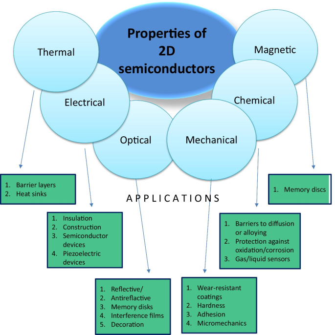
일반적인 응용 분야에서 활용되는 2D 반도체의 특성
주목할 만한 점은 2D 나노구조 반도체 분야가 나노 제조의 최신 기술 발전으로 인해 현대의 고성능 나노 및 광전자 기기 개발을 위한 중요한 지식으로 독립적으로 자리 잡고 있다는 점입니다[45]. 2D 나노물질의 원자 규모 계층 구조는 고유한 특성의 기원이며, 여기서 물질 특성의 정확한 조정 가능성은 치수의 원자 수준 제어에 의해 제공됩니다. 따라서 균일한 두께의 초박형 2D 필름의 등각 합성은 2D 나노 물질을 기반으로 하는 첨단 전자 기기의 제조 방법 개발을 위한 기본 단계로 매우 바람직합니다. 특히, 원하는 기판 위에 정밀하고 균일한 두께의 웨이퍼 스케일 초박막을 생산하기 위해서는 2D 반도체 기반 기기 제작을 위한 성공적인 합성 기술이 개발되어야 한다[46]. 또한 합성 및 제조 단계에서 2D 나노 물질을 장식할 수 있으며 다양한 기하학적 특징을 가진 전도체, 절연체 및 기판을 포함한 전자 장치의 다양한 구성 요소와 직접 접촉할 수 있습니다. 또한 2D 나노물질과 다른 구성 요소 사이의 이종 계면이 그 속성에 근본적으로 영향을 미칠 수 있다는 점을 고려해야 합니다. 이것은 특히 2D 층 사이의 전하 전달 메커니즘과 관련이 있습니다[47]. 이종 구조 2D 필름의 고유한 기능은 이종 구조 전자, 광전자, 바이오 센싱, 환경 센서, 촉매, 웨어러블 및 플렉서블 전자, 멤리스터 및 시냅스 장치를 포함한 많은 응용 분야에서 사용할 수 있습니다. [36, 44, 48 ,49,50,51,52,53,54,55]. 따라서 합성 및 제조 기술은 차례로 2D 나노 물질을 기반으로 하는 기능 기기의 제조 복잡성에 대응해야 합니다. 또한 2D 재료의 전자적 특성은 물리적 및 화학적 구조, 치수, 층 수, 형태, 방향, 구조상, 도핑 결함, 비정질 또는 결정도, 구조의 결정립계를 비롯한 재료 특성에 크게 영향을 받습니다. [56]. 2D 나노구조의 층 수는 전자 구조에 추가적인 근본적인 영향을 미치며 2D 재료의 특성은 2D 필름을 기반으로 하는 전자 장치의 최종 성능을 완전히 결정합니다[57].
반면에 2D 재료의 결정도 또는 비정질도 전자 특성을 변경할 수 있습니다. 합성 방법과 조건에 따라 결정되는 2D 나노물질은 결함이 없는 (단결정) 또는 약간의 불순물 수준을 포함하거나 입자 경계가 거의 없습니다. 따라서 계면 산란 현상을 통한 전하 이동도는 결정립계의 수에 의해 영향을 받는다[58]. 단결정 구조가 가장 높은 전하 이동도와 낮은 계면 산란을 갖는 반면, 비정질 2D 구조는 가장 높은 절연 특성을 나타냅니다[58]. 2D 나노 물질의 초기 합성 방법의 대부분은 2D 나노 구조의 기계적 박리를 기반으로 했습니다. 층상 구조 사이의 약한 vdW 힘으로 인해 기계적 및 화학적 박리가 층상 2D 나노 구조를 추출하는 데 효과적으로 사용될 수 있습니다 [59]. 따라서 기계적 박리는 호스트 재료에서 고품질 결정질 2D 구조를 분리합니다. 그러나 기계적 박리는 이미 대규모 2D 나노 필름을 합성하는 데 실패했습니다. 유사하게, 2D 재료의 액상 박리는 2D 재료의 저비용, 대규모 생산에 적합한 또 다른 접근 방식입니다. 그럼에도 불구하고, 품질 관리와 크기 균일성은 이 박리 기술을 통한 2D 필름 합성의 주요 과제입니다[58]. 반대로, 기상 증착 기술을 통한 2D 필름의 직접 성장은 정밀한 치수 제어로 고품질 웨이퍼 크기의 2D 나노 필름을 제조하기 위한 가장 신뢰할 수 있고 적용 가능한 합성 방법 중 하나로 밝혀졌습니다. 예를 들어, CVD와 ALD는 나노구조의 2D 반도체와 이종구조의 대면적 제작에 뚜렷한 기술적 이점을 제공하는 두 가지 주요 기상 기반 증착 기술입니다[60, 61]. 두께, 화학적 조성, 결정화도 상태, 도핑 요소 및 구조적 결함의 비율에 대한 정확한 제어는 각각 CVD 및 ALD 공정에서 성장 매개변수를 주의 깊게 조작하여 적절하게 달성할 수 있습니다. 또한, 2D 필름의 기존 합성 방법과 별도로 몇 년 전에 다른 새로운 2D 재료 소스가 등장했습니다. 예를 들어, 액체 금속의 표면 산화물은 실제로 액체 합금의 물리적 및 화학적 특성에서 발생하는 전례 없는 특성을 가진 고품질 천연 2D 나노필름의 고유한 소스입니다[61].
결과적으로 이 리뷰에서는 ALD 및 CVD 기술과 액체 금속의 2D 표면 산화물의 vdW 박리에 초점을 맞춰 2D 나노물질의 새로운 합성 방법에 대한 최신 연구 결과를 논의할 것입니다. 기상 증착 기술에서 2D 재료의 성장 메커니즘을 설명하고 2D 기반 반도체 재료의 제조 및 증착에 있어서의 주요 과제와 기회에 대해서도 논의합니다. 또한, 최근에 개발된 액체 금속의 2차원 자연 표면 산화막의 vdW 박리 기술을 소개합니다. 마지막으로 최신 전자 및 광전자 특성을 포함하여 초박형 2D 기반 장치의 개발된 기능 응용 프로그램을 자세히 설명하고 특성화합니다.
2D 반도체 재료 분야에서 연구의 주요 초점은 2D 나노구조의 합성 및 특성화입니다. 이러한 2D 나노구조는 원자 및 얇은 두께의 광범위한 무기, 유기 및 고분자 재료에 속합니다. 합성 전략은 일반적으로 두 가지 주요 접근 방식, 즉 하향식을 따릅니다. 및 상향식 전략. 따라서 제어된 아키텍처와 물리적, 화학적 특성을 가진 2D 반도체의 개발은 다양한 응용 분야에서 핵심적인 역할을 하며 오늘날의 상업용 반도체 기술보다 훨씬 높은 수준으로 새로운 가능성을 열어줄 것입니다. 그럼에도 불구하고 지난 몇 년 동안 2D 반도체에 대한 상당한 노력과 독특한 과학적 발견에도 불구하고 대부분은 산업 응용 분야에서 사용할 수 없는 매우 간단한 박리 기술을 사용하여 실험실에서 얻어졌습니다. 한 가지 대안은 하향식을 나타냅니다. 일반적으로 층상 재료 및 층상 공유 유기 프레임워크(COF)의 박리 및 vdW 박리를 포함하는 방법입니다. 그러나 이 방법의 병목 현상은 제품 수율이 매우 낮고 응고 중에 시트가 다시 쌓이는 것입니다. 또 다른 대안은 상향식을 기반으로 합니다. 2D 방식으로 무기, 유기 또는 고분자 전구체의 이방성 조립. 2D 나노 물질의 제조에 어느 정도 성공했지만 전기화학적 에너지 저장 및 변환에서 다양한 기능을 가진 합리적으로 설계된 2D 나노시트에 대한 심층 조사는 여전히 원시적입니다. 따라서 다양한 응용 분야에서 이온 확산 및 전자 수송을 가속화하기 위해 맞춤형 두께, 높은 표면적, 우수한 전도성 및 기계적 유연성을 가진 2D 나노 물질의 고유성에 대한 완전한 탐구가 매우 요구될 것입니다. 다음 섹션에서는 지난 몇 년 동안의 성과에 초점을 맞춰 2D 재료의 두 가지 주요 증착 기술, 즉 CVD 및 ALD의 기본 사항을 개괄적으로 설명합니다.
초박막의 기상 기반 직접 성장은 초정밀 치수 사양의 고품질 필름 증착을 위한 가장 신뢰할 수 있고 적용 가능한 합성 방법 중 하나입니다[62]. 다양한 방법 중에서 CVD는 여러 다른 기판에 초박형 2D 필름을 성장시키는 잘 알려진 최초의 성공적인 기술입니다. CVD는 고품질 대면적 2D 필름의 성장을 위한 확장 가능하고 제어 가능한 접근 방식을 제공합니다[63]. CVD 방법을 2D 나노 물질의 제어 가능한 증착을 위한 신뢰할 수 있는 기술로 만드는 몇 가지 고유한 사양이 있습니다. 이 방법은 기체 상태의 기체 물질이 기판 표면에서 단계적으로 반응하는 방식을 기반으로 합니다. CVD 반응은 원자층 두께가 거의 없는 고체 상태 박막의 성장으로 이어집니다. 따라서 2D 나노물질의 특성은 계면 특성, 기판의 기하학적 특성 및 고체 필름의 구조적 위상에 크게 의존합니다. 이러한 특성은 CVD 성장 매개변수의 정확한 조정에 의해 신중하게 조절될 수 있습니다. CVD 성장의 일반적인 메커니즘을 이해하려면 온도, 압력, 기판 및 전구체를 포함한 CVD 매개변수가 표면의 물질 전달, 열 전달 및 계면 반응에 어떻게 영향을 미칠 수 있는지 이해해야 합니다. 이와 관련하여 공정 중 주요 증착 매개변수를 제어하는 잘 설계된 레시피가 개발되어야 합니다[64]. 또한 2D 나노필름의 도핑 수준을 제어할 수 있으며 이는 특정 특성을 가진 반도체 나노구조 설계에 필수적인 기능입니다[64]. 예를 들어, CVD 공정 동안 칼코겐 및 금속 결손의 수준을 제어하는 것이 가능합니다. CVD 공정의 다음 주요 매개변수는 구조상, 형태 및 계면 반응에 크게 의존합니다.
온도는 전구체의 화학 반응 속도, 캐리어 가스의 유속, 그리고 마지막으로 CVD 막의 성장 속도에 영향을 미치는 등 CVD 막 성장 동안 여러 상호 연결된 요소에 직접적인 영향을 미치는 주요 기본 매개변수 중 하나입니다[64]. 일반적으로 높은 CVD 온도는 고품질 2D CVD 필름의 증착을 보장합니다. 그러나 극도로 높은 온도에도 단점이 있습니다. 특히, 높은 농도 구배를 생성할 수 있으므로 시스템에서 불안정한 질량 흐름 및 이동을 유발할 수 있습니다[64]. 또한 챔버의 구성 요소 포화 압력에 직접적인 영향을 미치므로 결과적으로 박막의 성장 속도가 변경됩니다. 온도와 압력의 결합된 효과는 2D TMDC 필름의 CVD 증착 동안 관찰될 수 있습니다. 이러한 유형의 2D 나노구조에서 시스템의 황 및 셀레늄 원소의 농도는 2D 필름의 최종 구성을 결정하는 데 매우 중요합니다. 예를 들어, 높은 가스 압력과 농도는 2D TMDC(MoS2 , WS2 , 등.). 일반적으로 높은 CVD 온도는 열역학적으로 활성화된 증착 메커니즘을 용이하게 하는 충분한 압력을 수반하는 반면 낮은 CVD 온도는 일반적으로 동역학적 성장 프로세스로 이어집니다[64, 65]. 제어된 성장 메커니즘은 속성 및 다수의 기본 레이어를 조정할 수 있는 기능을 갖춘 2D TMDC의 제어된 성장을 최종적으로 초래합니다.
CVD는 공정 압력이 대기 수준에서 수 밀리미터로 변경될 수 있는 가변 압력 증착 기술로도 알려져 있습니다. 제어 가능한 CVD 공정에 가장 유리한 조건은 대량 공급의 저농도 및 고속에서 달성됩니다. 이와 관련하여 저압은 TMDC 2D 나노구조의 웨이퍼 규모 증착에서 초박형 2D 나노구조의 균일한 성장을 위해 항상 더 신뢰할 수 있습니다[66, 67]. 부품의 부분압은 또한 2D TMDC 필름의 균일한 층별 성장에 직접적인 영향을 미칠 수 있습니다. 따라서 2D MoS2의 성장은 CVD 기술에 의한 막은 가장 유명한 예 중 하나이며, 초기 성장된 막 위에 두 번째 기본 레이어의 제조가 저압에서 첫 번째 증착된 레이어의 결정립계에서만 시작될 수 있습니다.
기질의 특성은 2D 필름 및 이종 구조의 성장에 근본적인 영향을 미칩니다. 예를 들어, 금속 기판, Si, SiO2 , 운모 및 폴리이미드는 2D 필름의 CVD 증착에 가장 일반적으로 사용되는 기판 중 하나입니다[68, 69]. 2D 필름의 성장 메커니즘에서 기판의 역할은 결정성, 결정립 방향, 미세 구조 및 특성을 결정합니다. 특히, 금, 니켈, 구리 및 은 기판에 증착된 2D 금속 산화물 필름은 촉매 활성 특성을 보여주었습니다[70,71,72]. 일반적으로 금속 기판의 경우 특정 결정 방향을 가진 2D 필름의 우선적인 성장은 기술적으로 금속 기판과 증착된 TDMC 필름 사이의 면 의존적 결합 에너지에 의존합니다[73]. 또한 성장한 나노구조의 형태에 직접적인 영향을 미칩니다. Au 박막에 2D 금속 산화물 증착의 경우 Au와 산소(O), Au와 2D 산화막의 금속(M) 성분 사이의 결합 에너지에 따라 Au와 금속 산화물 박막 사이의 이종계면에서 화학적 결합 구조가 결정된다. [73]. Au와 산화막의 금속 원자 사이의 우선 결합이 예측되며, 대부분 Au-M-O 계면의 형성을 초래합니다[74,75,76]. Au 또는 기타 금속 기판과 증착된 산화물 박막 사이의 강한 상호 작용은 금속 기판의 결정 구조로부터 2D 산화물의 적응 성장을 가능하게 했습니다[77,78,79]. 이는 제1 금속 산화물 단분자막의 성장 패턴이 금속 기판의 결정 패턴을 따른다는 것을 의미한다. 예를 들어, Au는 면심 입방체(fcc) 결정 구조를 가지고 있지만 Au 기판 표면의 결정 방향은 2D 금속 산화막의 결정 방향을 결정합니다. 주목할만한 점은, 구성되지 않은 Au(111)는 육각형 격자로 구성되어 있는 반면 재구성된 Au(111) 평면은 복잡한 구조를 보여줍니다[80, 81]. Au 기판에 증착된 다양한 산화막이 Au(111) 패싯과 초박막 산화막 사이의 강한 상호작용에 의해 야기된 헤링본 재구성을 들어 올리는 것이 관찰되었습니다. 몇 가지 다른 2D 금속 산화물이 TiOx를 포함한 Au 기판에서 성장했습니다. , VOx , CoO, MoO3 , MgO, ZnO 및 WOx [82]. 유명한 촉매 예 중 하나는 2D TiO2입니다. Au(111) 기판 [83]의 표면에서 성장. Ti 원자는 Au 격자의 3중 중공 부위를 차지하고 O 원자는 Ti 원자의 브리지 부위에 위치하며, Ti2 O3 그림 3a[83]와 같이 형성됩니다. 또한, M-O 격자가 Au(111) 표면 위에 중첩되어 무아레를 형성하는 2D 산화막의 또 다른 성장 메커니즘이 있습니다. TiO stoichiometry를 사용하여 바람개비 구조의 다른 모양의 성장을 초래하는 패턴은 각각 그림 3b와 c에 나와 있습니다[83]. 육각형 무아레 패턴 성장은 Au(111) 기판의 TiO, FeO[84], CoO[85] 및 ZnO[86] 초박막의 CVD 동안 일반적으로 관찰되었습니다.
<그림>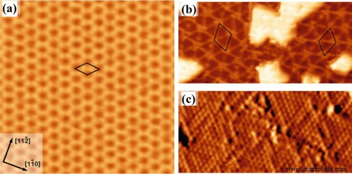
a의 STM 이미지 벌집 Ti2 O3 구조 및 b Au(111)에서 성장한 바람개비 TiO 단층 및 c Au의 바람개비 구조의 원자 분해 STM 이미지(111). [83]의 허가를 받아 복제
모스2 는 2D TMDCS 제품군의 전형적인 대표자입니다. 지금까지 그것은 벌크 물질과 단일 층에 대해 각각 1.29 eV와 1.90 eV의 상대적으로 작은 밴드 갭을 가지기 때문에 모든 TMDCS 중에서 가장 유리한 나노 물질 중 하나로 간주되었습니다[40, 87, 88]. 이전에는 단결정 MoS2 2D 필름은 호스트 벌크에서 기계적으로만 박리되었습니다. 직접 갭 반도체이기 때문에 MoS2의 단일 레이어 이론적 한계인 60mV dec −1 보다 더 날카로운 턴온을 특징으로 하는 대역간 터널 전계 효과 트랜지스터(FET) 구현을 위한 흥미로운 가능성 제공 고전적인 트랜지스터의 경우 결과적으로 더 작은 전력 손실이 발생합니다. 이 기능은 간접 갭 반도체인 실리콘의 경우 달성하기 어려운 상태로 남아 있습니다. 그 이유는 대역 간 전이가 포논과 재결합 중심을 필요로 하기 때문입니다[87]. 2D MoS2의 흥미로운 최근 애플리케이션 중 하나 나노결정은 MoS2의 단일 레이어를 기반으로 하는 트랜지스터[87] 및 포토트랜지스터[40]입니다. 나노시트. 또한 MOCVD(금속-유기 화학 기상 증착), LPCVD(저압 화학 기상 증착), ICP-CVD(유도 결합 플라즈마 화학 기상 증착)를 포함한 수정된 CVD 기술을 통해 2D 필름의 성공적인 대면적 증착이 이루어졌습니다. ), 또는 다른 기술에 의해 개발되고 결합된 기타 혁신적인 방법. CVD는 2D TMDC 필름의 웨이퍼 규모 증착 능력으로도 잘 알려져 있습니다. 그림 4는 흥미로운 예 중 하나가 초박형 2D MoS2의 라거 영역 증착을 보여줍니다. 및 WS2 4인치 웨이퍼 위의 필름 [88]. 이 CVD 공정에서 Mo(CO)6 및 W(CO)6 및 (C2 H5 )2 S는 MOCVD 기술의 전구체로 사용되었지만 H2 /Ar은 MOCVD 공정에서 캐리어 가스(그림 4a, b)로 사용되었습니다[88]. 2D MoS2를 기반으로 하는 8100개의 고성능 FET 유닛이 동일한 백 게이트 기판으로 포토리소그래피 기술을 사용하여 필름을 제작했습니다(그림 4c). 장치의 두 번째 구성에서 외부 SiO2 유전체 필름이 2D MoS2에 증착되었습니다. FET 기기를 제작하기 위한 필름(그림 4d). 트랜지스터의 전기적 측정은 다른 웨이퍼 부품에서 선택된 FET의 일관된 성능을 확인했습니다. 따라서 2D MoS2의 CVD 공정 동안 균일하고 등각적인 성장 조건 및 WS2 필름이 확인되었습니다(그림 4f).
<그림>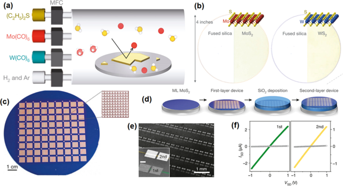
MoS2의 웨이퍼 규모 MOCVD 성장 지속 및 WS2 영화. 아 CVD 장치 및 2D MoS2의 MOCVD 관련 전구체의 그래픽 개략도 및 WS2 영화. ㄷ 2D MoS2 기반 8100 FET 장치 배치 Si/SiO2 위의 필름 웨이퍼. 삽입된 이미지는 100개의 장치를 포함하는 1mm 정사각형의 확대된 이미지를 보여줍니다. d 적층 MoS2의 순차 제작 단계 기반 장치. 이 이미지는 MoS2를 보여줍니다. 첫 번째 및 두 번째 레이어의 FET 장치. 에 두 개의 다른 레이어에 있는 두 개의 인접한 FET 장치의 IDS-VDS. [88]의 허가를 받아 재인쇄
CVD는 또한 다양한 2D 이종구조를 제작하기 위한 다재다능한 기술로 자리 잡았습니다[89]. 예를 들어, CVD는 측면 및 수직 구성의 성공적인 증착을 위해 사용되었습니다. 측면 스타일에서 2D 나노 필름은 원자 수준에서 함께 부착되는 반면 수직 구조에서는 레이어 간의 상호 작용력이 vdW 특성을 갖습니다. 따라서 측면 2D 이종 구조에서 MoS2에 대해 보고된 바와 같이 2D 이종 인터페이스의 개발을 위해 엄격한 격자 일치가 매우 필요합니다. /WS2 헤테로 구조 [89]. MoS2의 1단계 간단한 증착 /WS2 측면 2D 헤테로구조는 황, 삼산화 몰리브덴 및 텅스텐 전구체가 CVD 공정 동안 사용될 때 확립되었습니다(그림 5a, b)[89]. 개발된 2D 필름은 원자 평면이 안락 의자 및 지그재그 방향과 동일한 결정 방향을 공유하는 날카로운 원자 헤테로 인터페이스를 가지고 있습니다(그림 5c). 필름의 최종 형태는 MoS2가 있는 삼각형 코어-쉘 모양이었습니다. 내부 및 WS2 외부(그림 5d). 라만 특성화 연구는 수직 및 측면 2D 필름의 제작을 확인했습니다(그림 5f). 개발 p-n 2D WS2 간의 이종 접합 및 MoS2 필름은 2D 헤테로 구조 필름의 광기전 효과를 강화했습니다. 따라서 강한 광발광 현상이 감지되었습니다(그림 5e, g)[89]. WS2와 유사한 동일한 결정 방향 및 격자 구조를 가진 상당히 날카로운 인터페이스 및 MoS2 2D 영화가 특징입니다. 또한, 다른 보고서에서 CVD는 측면 1H MoS2를 개발하기 위해 사용되었습니다. /1T' 모테2 두 구성 요소가 상대적으로 큰 격자 불일치를 갖는 이종 인터페이스 [90]. 2D WSe2를 포함하여 격자 불일치가 큰 2D TMDC 필름 사이의 이종 인터페이스의 개발을 보여주는 몇 가지 다른 사례가 있습니다. /MoSe2 [91] 및 MoS2 /WS2 반도체/반도체 측면 2D 헤테로 구조의 증착을 위한 CVD 방법의 능력 확인. 따라서 현대 CVD 기술은 유기 및 고분자 플렉서블 기판, 절연체 및 그래핀 기판에 2D 물질을 성공적으로 증착할 수 있는 다양한 기능을 입증했다고 결론지을 수 있습니다. 표 1은 웨이퍼 규모에서 CVD 기술로 제작된 2D TMDC와 이종 구조의 최신 성과를 요약한 것입니다[93].
<그림>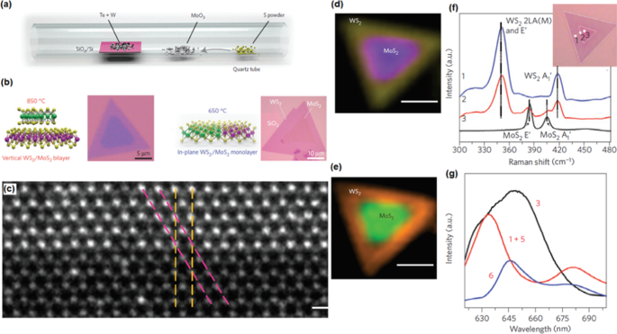
아 반도체/반도체 측면 2D 헤테로구조의 CVD 성장 개략도. ㄴ WS2 사이의 평면 내 인터페이스의 원자 해상도 대비 STEM 이미지 및 MoS2 . ㄷ 351cm −1 에서 2D 이종구조 2D 필름의 라만 강도 매핑 (노란색) 및 381cm −1 (자주색). d 630nm(주황색) 및 680nm(녹색)에서 결합된 PL 강도 매핑. [89]
의 허가를 받아 전재 및 복제일반적으로 CVD로 제작된 2차원 나노물질 및 이종구조의 안정성은 대부분의 발표된 연구에서 이러한 나노구조의 장기적 안정성에 대한 정보가 다소 제한적임에도 불구하고 상당히 높다. CVD 성장 TMDC 기반 전자 및 광전자 기기의 장기적인 성능과 안정성은 캐리어 산란 센터 역할을 하는 나노 물질의 계면, 결함 및 입자 경계에 의해 크게 영향을 받습니다. 이는 차례로 장치의 캐리어 이동성을 감소시킵니다. 따라서 깨끗한 표면, 고품질 및 웨이퍼 규모 도메인 크기를 갖는 2D 복합 재료의 준비는 미래의 나노 및 광전자공학에서 바람직한 목표가 되어야 합니다. 또한 많은 다른 2D 복합 재료가 아직 잘 연구되지 않았거나 성공적으로 성장하지 않았으며 결과적으로 더 흥미로운 발견이 발견되기를 기다리고 있음을 강조해야 합니다.
CVD의 수정으로서 ALD는 두께 제어 제조 2D 반도체 및 샌드위치형 이종 구조에 대한 다양한 전략을 구현할 수 있습니다. ALD는 약 45년 전에 처음 개발되었지만 21세기 초에 와서야 큰 장점과 다양한 전구체의 개발로 인해 더 인기를 얻었습니다[94]. 지난 10년 동안 산화물, 황화물, 셀렌화물, 텔루르화물, 질화물 및 금속을 포함한 다양한 유형의 재료 제조에 사용되었습니다[95]. 핵심 요구 사항은 적절한 분자 전구체가 자체 제한 반응을 거쳐야 한다는 것입니다. ALD와 다른 기상 증착 방법 간의 주요 차이점은 모든 전구체 노출 후에 자체 포화 표면 단층이 형성된다는 사실이기 때문입니다. ALD 화학의 최신 개발에 대한 완전한 설명은 최근 리뷰[94,95,96]에서 찾을 수 있습니다. 따라서 지금까지 ALD는 마이크로일렉트로닉스[97], 촉매 작용[98], 광전지[99] 및 센서[100]를 포함한 다양한 분야에서 구현되었습니다. Unfortunately, the ALD implementation toward the synthesis of 2D semiconductors and 2D sandwich nanostructures is rather limited.
As deposition technique, ALD consists of a series of self-limiting, surface-saturated reactions to form thin conformal films at a controllable rate. Despite all obvious ALD advantages, it has to be admitted that this emerging technology has not yet been fully exploited for fabrication of different 2D nanostructures. Apparently, the lack of reliable recipes and precursors, specific ALD temperature window for deposition are some of the valid reasons for that. On the other hand, it was recently reported that the ALD advantages are far superior to the existing capabilities of other deposition techniques [101]. Specifically, ALD is the only one technology, which enables fabrication of defects-free, conformal 2D nanofilms and their heterostructures on the wafer scale with precise, Ångstrom scale control of their thickness during deposition [102]. In this regard, the state-of-the-art nanoscale ALD interfacing and molecular engineering of 2D nanomaterials can open up completely new possibilities by providing ultra-thin channels for key doping, minimization of the density of interfacial impurities and optimization of capabilities of instruments. Furthermore, the ALD fabrication technique enables turning the design of 2D nanostructures toward heterojunctions and hetero-structures [103,104,105], and hybrid SE based on inorganic–inorganic [106], organic–organic and inorganic–organic nanomaterials [107]. Figure 6 illustrates growing interests to ALD as well as comparison of the deposition rates and properties for 2D nanostructures developed by various deposition techniques [94].

Number of annual citations on “Atomic layer deposition” topic a of published manuscripts. Data are according to Web of Knowledge™ Database. Comparison of the deposition rate vs step coverage (b ) and coverage areas produced by different deposition techniques (c ). Comparative analysis of properties of SE fabricated by PVD, CVD, and ALD, respectively (d ). Reproduced with permission from [94]
The layered TMDCs are composed of sandwiched structure where the metal layers covalently bonded with two individual surrounding chalcogen atoms, thus the layer-by-layer deposition mechanism in ALD technique is favourable for making layered 2D TMDC nanostructures. Among the different 2D TMDCs films including binary, ternary and doped chalcogenides, less than 20 type of them could be deposited via ALD method. The first MoS2 nanofilm was fabricated by ALD in 2015. Initially, the number of MoS2 layers was controlled by the tuning of parameters of ALD technique [106, 108,109,110]. Later, the ALD synthesis of TMDCs monolayer was reported [111,112,113,114]. The self-limiting layer synthesis (SLS) of MoS2 monolayer film was also facilitated based on the typical ALD half-reactions [115, 116]. Here, the some practical cases of ALD of stable 2D films of metal dichalcogenides are summarized in Table 2 [94].
The first investigation of 2D MoS2 deposition was based on the sulfurization of ALD deposited MoOx few-layered film. The formation of S–Mo-S arrangements of atoms along the z -axis was achieved after 10 min interaction of MoOx film with S gas at 600 °C [117]. The morphology, uniformity, crystallinity, nucleation and the quality of ALD-deposited film have direct impact on the final properties and characteristics of the MoS2 film [117,118,119,120,121]. In this example, the parameters of multistep annealing process should be controlled precisely to facilitate the formation of MoS2 films with sequential reduction of Mo and then incorporation of S atoms. In addition, the multistep reactions allowed the coverage control and phase transformation from crystalline MoS2 to the 2H-phase at the higher post-treatment temperatures. The first wafer-scale CVD of MoS2 on the 2-inch sapphire substrate was reported in 2014, when MoCl5 및 H2 S were employed as the precursors in the ALD system at 300 °C [121]. It was found that 10 sequential ALD cycles are required to establish the uniform growth of the MoS2 film and prevent the islands growth. The following post-annealing of ALD MoS2 film at 800 °C improved the crystallinity of MoS2 at the expense of losing the thickness uniformity of MoS2 on the wafer substrates. Thus, higher number of ALD cycles were done (20 cycles) to compensate the lack of uniformity due to the high-temperature post-annealing process. Considering the ALD window, it was found that the ALD process within 350 to 450 °C permits higher quality of sulfide layers with the growth rate of 0.87 Å/cycles [122]. It was also demonstrated that the following annealing of as-deposited MoS2 film in H2 S or sulfur gas can improve the stoichiometry of 2D MoSx film [123].
The deposition of 2D MoS2 films via ALD technique can also be achieved by usage of other precursors. Other main precursors for deposition of MoS2 2D films were Mo(CO)6 , H2 S and dimethyl disulfide compounds. The ALD window suitable for these precursors is in the range of 155–170 °C. By monitoring the mass gain during the ALD cycles, it was revealed that multiple pulses of Mo source are required to reach the saturation, while a single H2 S injection is sufficient to saturate the reaction and achieve the growth rate of 2.5 Å/cycle in the optimized condition [124]. The plasma-enhanced atomic layer deposition (PE-ALD) can also be successfully employed to deposit ultra-thin h -MoS2 film on the different substrates. The growth rate of 0.5 Å/cycle was observed at the ALD window of (175–200 °C) for deposition of 2D MoS2 영화. Lower ALD window (60–120 °C) caused the deposition of amorphous 2D MoS2 영화. Particularly, the ALD at 100 °C allowed the formation of continuous layer of amorphous MoS2 on the Si wafer. To improve the crystallinity of as-deposited ALD film, the later rapid thermal annealing (RTA) treatment at 900 °C led to the formation of crystalline hexagonal layer of MoS2 [125, 126]. Another recipe for deposition of 2D MoS2 film is Tetrakis (dimethylamido) molybdenum (Mo(NMe2 )4 ), which interacts with either H2 S or alternatively 1, 2 ethanedithiol (HS(CH2 )2 SH) to deposit 2D MoS2 영화. In this recipe, the ALD of MoS2 film taken place at the lower temperature (T < 120 °C) since the Mo(NMe2 )4 decomposes at temperature higher than 120 °C. The as-deposited 2D film was amorphous in this technique. Thus, the subsequent annealing was employed to crystalize the 2D MoS2 영화. The mass spectroscopy analysis revealed that the mechanism of ALD deposition of MoS2 film is based on the removal of the remaining NMe2 ligands from the substrate surface after interaction of sulfur gas with Mo precursor. It was roved that it is possible to deposited 2D films on polymeric substrates by using lower ALD temperature.
2D WS2 is another example of the layered dichalcogenide ALD deposited at 300 °C by using WF6 및 H2 S as precursors [127]. A Zn-based catalyst is required to initiate the deposition of WS2 film via ALD technique. Diethylzinc (DEZ) and H2 S were employed to assist the rapid nucleation of WS2 film over a wide range of substrates [128]. Zn acts as reducing agent for WF6 favouring the adsorption of WF6 on the surface of substrates. The initial growth rate of 1.0 Å/cycle was recorded, which then was reduced after 50 ALD cycles of WS2 침적. It was found that the deposition of a monolayer ZnS film is also facilitated the growth of WS2 film with crystalline structure [129, 130]
WSe2 is another TMDC 2D film which was fabricated by ALD [124]. In this report, a self-limiting approach for WCl6 and diethyl selenide (DESe) at the higher ALD temperature of 600–800 °C was employed and the dependence of film thickness on the ALD processing temperature was observed [131]. Five, three and one crystalized layers of WSe2 were deposited on the Si/SiO2 wafers (8 cm 2 ) at 600 °C, 700 °C and 800 °C, respectively. After 100 ALD cycles, the growth of WSe2 was stopped due to growth saturation. The deposited WSe2 film with few layers and monolayer was crystallined with honeycomb structure. The same film was employed as a p -type semiconductor in the FET and showed the capability of ALD deposited WSe2 film for application in electronic devices. In another parallel attempt, the thermal ALD of continues WSe2 film on the Si/SiO2 substrate was successfully carried out at 390 °C [132]. WCl5 및 H2 Se were employed to deposit a highly uniform film with well-crystalline structure. The quality and crystallinity of the ALD WSe2 film were fairly compatible to the mechanically exfoliated and CVD WSe2 films [132].
SnSx 2D family is the other types of 2D materials which was extensively studied during last few years. The first deposited SnS film was reported by using tin (II) 2,4-pentanedionate (Sn(acac)2 ) precursor as the Sn source and H2 S as the sulfur source, respectively, where the growth rate of 0.23 Å/cycle was achieved in the ALD window from 125 to 225 °C. The other precursors for ALD of SnS film are bis(N ,N ’-diisopropylacetamidinato) tin (II) (Sn(amd)2 ) and N2 ,N3 -di-tert-butylbutane-2,3-diamine tin (II) which react with H2 S gas during ALD [133]. This recipe enabled the deposition of crystalline SnS film at the ALD temperature of less than 200 °C.
2D SnS2 and SnSx films are deposited via employment of precursors containing Sn atoms [134]. The tetrakis (dimethylamino) tin (TDMASn) [135, 136] and tin acetate (Sn(OAc)4 ) [137] as the Sn (IV) metal precursors were used for ALD of SnS2 영화. Polycrystalline hexagonal SnS2 films were deposited with the growth rate of 0.64–0.8 Å/cycle [134] at the temperature range of 140–150 °C. The growth of ALD temperature above 160 °C resulted in the development of thin mono-sulfide films. However, the as-deposited film always contains a combination of both mixed SnS and SnS2 화합물. Crystallinity of the film can still be improved by the following post-treatment annealing in H2 S gas at 300 °C. As an example, the formation of a single phased orthorhombic 2D SnS2 films with interlayer spacing of 0.6 nm was reported after the post-annealing treatment at 300 °C in H2 대기. Another precursor for ALD deposition of SnS2 film is Sn(OAc)4 where the ALD reaction in the ALD temperature of 150 °C resulted in the growth rate of 0.17 Å/cycle for the amorphous stoichiometric SnS2 영화. Generally, in ALD deposition of few-layered SnSx films with Sn precursors and H2 S gas, the chemical composition, structure and the stoichiometry of SnSx ALD structures can be modulated depending on the deposition conditions and the post-ALD treatments [137].
One of the main ALD capabilities is the wafer-scale deposition of 2D hetero-structured TMDCs, which opens up further opportunity for fabrication of vdW hetero-structures. The technological challenges for deposition of 2D hetero-structured films are the main concerns for their deposition. Basal plans of the most of 2D materials are inert with the lack of dangling band, thus the nucleation of 2nd family of 2D films over the first layer is considerably challenging. Therefore, it is necessary to enable the initial adsorption of precursors on the surface of 2D film and then facilitate the growth of second 2D film over substrate. One of such examples is the ALD deposition of Sb2 테3 film on the surface of graphene by using SbCl3 and (Me3 Si)2 Te as precursors [138]. In this ALD process, (Me3 Si)2 Te was initially physically adsorbed on the graphene. The successful low deposition temperature of 70 °C for ~24.0-nm-thick crystalline Sb2 테3 layer was finally achieved with the crystalline plane parallel to the graphene substrates. A sharp hetero-interface was formed between the graphene and Sb2 테3 film as depicted on the high resolution transmission electron microscope (HRTEM) image in Fig. 7a [138].

아 Cross-sectional image from the interface between ALD grown Sb2 테3 그래핀/SiO2에 기질. ㄴ The cross-sectional image of heterostructured Sb2 테3 /Bi2 테3 stacked layers. ㄷ The HRTEM image of SnS/WS2 heterointerfaces and d the corresponding fast Fourier transform (FFT) image. Reproduced with permission from [138]
In another attempt, 2D hetero-structured Sb2 테3 /Bi2 테3 metal chalcogenides films were deposited by the ALD process on Si/SiO2 wafer. Here, the bismuth telluride was selected to be deposited over the silicon wafer by the ALD technique at 165–170 °C, since it covers the Si better than Sb2 테3 . Considering the low ALD temperature of Bi2 테3 (at 65–70 °C), the employment of initial long SbCl3 pulse in the ALD chamber was taken as a capable strategy to saturate the surface of Bi2 테3 and complete the surface reactions for the next deposition step [139]. This approach also facilitated the disposition of three stacking layers of Bi2 테3 /Sb2 테3 with a high level of crystallinity. Another example is the growth of multiple WS2 /SnS layered semiconductor hetero-junctions on the Si/SiO2 substrates by alternating ALD of WS2 and SnS at the ALD temperature of 390 °C [140]. The stacked 2D WS2 /SnS has the 15° orientation angle between their c axis originated from the difference in crystalline structures and the lattice mismatch between WS2 and SnS (Fig. 7b, c) [133]. This misaligned crystalline characteristics of WS2 /SnS hetero-interfaces is the origin of noticeable decreased of the holes mobility in SnS film [140]. Generally, the ALD techniques are recently undergoing consistent progress to enable the deposition of higher numbers of 2D TMDC films. However, there are still countless research opportunities to develop suitable ALD recipes for deposition of 2D TMDC films over the different substrates and also to develop nanoelectronic instruments based on 2D TMDCs.
The few-nanometer-thick metal oxide films can be considered as 2D nanostructures when they can be assigned to few layers of 2D films. In this context, the characterization and exploration of 2D oxides properties for the practical applications are considered as valuable technical knowledge along with the progressive advancement in the device miniaturization. Furthermore, modern technologies use the advantages of ultra-thin metal oxide nanostructures as the main components of state-of-the-art nanodevices. Consequently, promising applications for the ultra-thin 2D semiconductors and insulators are expected, such as solid oxide fuel cells, catalyst films, corrosion protection layers, chemical sensors, spintronic devices, and UV and visible light sensors. Metal oxide semiconductor field-effect transistors (MOSFET) and the other novel nanoelectronic instruments are fundamentally dependent on the ultra-thin uniform films of metal oxides. Complementary, metal oxide semiconductor (CMOS) sensors are technically developed based on the deposition of ultra-thin metal oxide films which opened up a quite number of the different applications from image and light sensors to FET transistors in low-energy semiconductor instruments. The solar energy cells, plasmonic devices, data storage applications, bio-compatibility and bio-sensing features, supercapacitance properties, and electrochemical sensing are among the recently announced and discovered applications of the 2D oxide semiconductors. Thus ALD deposition of 2D metal oxide semiconductor thin films is considered as advanced fabrication technology. It is also an extremely difficult target to achieve considering the fact that the structural stability and molecular integrity of 2D films can be deteriorated easily. Accordingly, one of the main challenges is the versatile and conformal deposition of these 2D oxide nanostructures on the convenient substrates [94]. The following section is specifically focused on the ALD of metal oxide materials, and particular attention is given to molybdenum, titanium, aluminum, and tungsten oxide 2D films.
Distinguishable properties of nanostructured molybdenum trioxide (MoO3 ) made it an excellent candidate for catalytic, electrical and optical applications. There are also several promising functionalities originated from the heterointerface between the MoO3 semiconductor and their metallic substrates. The bis(tert-butylimido) bis(dimethylamido) molybdenum ((tBuN)2 (NMe2 )2 Mo) is one of the precursors for MoO3 deposition, since it provides good volatility and thermal stability [141]. The PEALD window for molybdenum oxide with O2 plasma and ((tBuN)2 (NMe2 )2 Mo) precursor is in the range of 50–350 °C. The as-deposited films fabricated at the temperatures below 250 °C are usually amorphous, thus the post-deposition annealing process is needed to experience a transition from the amorphous to crystalline state. While the as-deposited films are sub-stoichiometric, the stoichiometry can be adjusted by the modulation of plasma parameters. The other precursors for ALD of ultra-thin MoO3 film is Mo(CO)6 which is mostly employed via O2 plasma to facilitate the low-temperature PE-ALD of MoO3 films in the narrow ALD window of 152–172 °C [141]. The resulted MoO3 film was deposited with growth rate of 0.75 Å/cycle. The as-deposited film was found amorphous with the oxygen deficiency at the heterointerface between substrate and MoO3 영화. To achieve the crystalline structure, the following post-annealing at temperature above 500–600 °C is required. In another strategy, the ozone plasma was used on the surface of ALD MoO3 film deposited on 300 mm Si/SiO2 wafer [141]. Mo film was fabricated by using Si2 H6 and MoF6 precursors at 200 °C. The wafer-scale deposition of ultra-thin MoO3 film over 4-inch Au on the Si/SiO2 wafer was reported, where C12 H30 N4 Mo as molybdenum precursor and O2 plasma as oxygen source were used at two ALD temperatures of 150 and 250 °C, respectively. The process includes the pre-exposure of bare Au surface by O2 plasma which assists the formation of OH bonding on the Au surface. The following chemisorption of C12 H30 N4 Mo molecules by the active sites on the Au and interaction with OH group on the surface of Au film led to the ligand exchange. The following O2 plasma completed the oxidation process and finalized the growth of ultra-thin monolayer MoO3 film (Fig. 8). The development of Mo–O-Mo bonding is expected after completion of oxidation process. Finally, 4.6-nm-thick MoO3 film was deposited over the wafer substrate. In this technique, the growth rate from 0.78 Å/cycle to 1.21 Å/cycle was measured when the ALD temperature increased from 150 to 250 °C [141].

아 Graphical scheme of deposition of 2D MoO3 nanofilms by PE-ALD. ㄴ The injection of precursor into ALD chamber and c the reaction between precursor and Au surface (d ) and the complete deposition of a monolayer film over Au substrate. 이 The thickness of PE-ALD MoO3 film over Au substrate vs. the ALD cycle number at based on the usage of (NtBu)2 (NMe2 )2 Mo precursor and O2 plasma at 150 °C and 250 °C, with the precursor dosing time of 2 s and plasma exposure time of 5 s. 에 The saturation curve of (NtBu)2 (NMe2 )2 Mo precursor. The GPC is demonstrated as the function of precursor dosing time. 지 The saturation curve for O2 plasma showing the GPC as the function of plasma exposure time. Reproduced with permission from [141]

Enhancement of non-stoichiometry in monolayer WO3 film developed by ALD via intercalation/de-intercalation process
Wafer-scale deposition of ultra-thin titanium dioxide (TiO2 ) film on the Si/SiO2 substrate was achieved by using the using tetrakis (dimethylamino) titanium (TDMAT) precursor and H2 O as an oxidation agent [145]. The optimum ALD temperature of 250 °C was selected for ALD of monolayer TiO2 film on the wafer-scaled substrate. To achieve a complete coverage of monolayer TiO2 , two individual ALD super-cycles were designed and implemented [145]. The first super-cycle consisted of 10 consecutive cycles of pulse/purge TDMAT to assure the reliable coverage of surface by precursors. Afterward, 10 pulse/purge stages of H2 O were performed to assure the completion of oxidation [145]. The XPS studies confirmed the changes of binding energies in both Si 2p and Ti 2p peaks after the deposition of 2D TiO2 could be elucidated by the development of Si–O–Ti bonds at the interface between native SiO2 and deposited 2D TiO2 영화. The deposition of TiO2 SiO2에 substrate was accompanied by the decrease in binding energy of Si 4+ which was related to this fact that the silicon was more electronegative than titanium. The evidence of oxygen bridge bonding was also demonstrated by characterization of vibrational mode of Ti–O–Ti bonds in the FTIR spectrum of monolayer TiO2 and also by investigation of XPS spectrum of monolayer film [145]. The bandgap of 3.37 eV was measured for this TiO2 film with atomic-scale thickness. The capability of ALD for deposition of ultra-thin films is of great importance to functional applications like microelectronics and catalysis where only few ALD cycles are desirable. Table 3 summarizes practical cases for ALD development of various 2D metal oxides reported to date.
In regard to stability of the ALD fabricated 2D nanostructures and their heterointerfaces, its mainly depends on the surface chemistry of ALD of 2D materials, especially because the inertness of their basal plans is expected to inhibit their growth and thus formation of vdW heterostructures. Moreover, as each precursor has specific “ALD window ” of deposition temperatures, trials and errors approach is required for optimization of the ALD fabrication temperature for each specific precursor taking into account the final thickness and porosity of deposited materials [98, 109]. Owing to the low deposition temperature, ALD of 2D oxides usually leads to fabrication of amorphous layers [32, 94]. Hence, when the crystalline phases of metal oxides are needed, post-annealing treatment is generally applied, improving the crystalline quality of the films as well as the interfaces with the substrate, which ultimately leads to the better stability of 2D nanomaterials over the time. Finally, although ALD appears to be a method of choice to fabricate oxide monolayers due to its precise control of the film thickness, only a handful of reports can be found in the literature [21, 32, 98, 141, 144, 145]. Therefore, the area of 2D metal oxide and their hetero-interfaces fabricated by ALD remains rather unexplored.
The library of novel 2D materials for advanced applications is currently limited by the conventional synthesis methods of 2D films. The mechanical exfoliation of 2D films from their host layered bulks is not technologically precise and attractive method since the sizes distribution and thickness of produced nanosheets are not adequately and accurately controlled [146]. While the high vacuum techniques are accuracy of the depositing films are considered as high-quality films, these methods are still expensive, time consuming, and restricted by availability of precursors [64]. On the other hand, it is always desirable to introduce new synthesis methods of 2D materials in order to obtain the advanced 2D nanostructures with superior properties. Thus, synthesis of novel 2D semiconductor materials with distinguished or improved characteristics still remains a fundamental challenge.
Room-temperature liquid metals are a group of metals and alloys with unique electron-rich metallic cores which let them to stay in the liquid states even at the room temperatures. The interface of liquid metals with surrounding environment is the origin of one of the most natural 2D films [147]. This self-limiting surface oxide films (skin) is one of the most perfect planar materials with atomic scale thickness [148]. These crystalline structures are the host of unique properties and have provided a novel platform for synthesis of high-quality thin-film 2D materials for advanced applications [149]. Here, the liquid metals have the role of host material for synthesis of 2D films. With respect to the atomic structure, elemental composition, fluidity and thermodynamic of liquid metals, and furthermore, by considering the nucleation and growth characteristics of the surface oxide films, countless parameters are engaged to determine the proprieties of extracted 2D surface oxide films [150]. The low melting monophasic metal alloys are composed of post transition metals (Ga, In, Sn, Pb, Al, and Bi) and the elements of group 12 (Zn, Cd, and Hg). These elements can be combined together to produce a group of liquid alloys with low melting temperature. A biphasic liquid metal (mixture of solid and liquid) can be formed by either deviation of alloy composition from eutectic point or via adding solute elements above the solubility limit into the liquid metal solvent [151]. Gallium (Ga) is one of the most famous liquid metals with room-temperature melting point and possessing both covalent and metallic bonds at the solid state. The strong structural anisotropy and weak atomic bonding between Ga dimmers is originated from the distance between Ga neighbour atoms 2.7–2.9 Å which is considered as a significant distance between the gallium dimers [152]. This weak atomic bonding results in the weak crystalline structure in gallium which can easily break up at the room temperatures [153]. The alloying of Ga with some of the other elements may lead to further decrease in melting temperature of liquid alloy. One of the famous examples is the Ga-In alloy, when the melting temperature decrease to 16 °C in eutectic point of In-Ga alloy with atomic concentration of 14.2% indium [153]. The interface between gallium alloy and surrounding atmosphere is composed of the atomic-scale-thick gallium oxide (Ga2 O3 ). The liquid metal reacts with atmospheric oxygen even at very low oxygen pressure forming a self-limiting metal oxidation reaction [153]. This ultra-planar oxide films are among the most perfect naturally grown 2D materials [61]. This natural film prevents the liquid metal from the further oxidation. The ionic transfer through the natural surface oxide film is the controlling factor for the natural growth of surface oxide films of liquid metal and alloys. The formation of this oxide film leads to the highest reduction in the Gibbs free energy (ΔG f ) [154]. In a liquid metal alloy, the surface oxide film is mostly composed of surface oxide films of one of elemental oxide films of alloy components. The most famous example is the surface of oxide film of galinstan alloy. Galinstan (EGa, In, Sn) is the eutectic alloy of gallium–indium–tin. However, the surface oxide of galinstan is composed of Ga2 O3 . Since the ΔG f of Ga2 O3 is lower than that of In2 O3 및 SnO2 in oxygen atmosphere, the surface oxide of galinstan alloy is mostly composed of Ga2 O3 [155]. With the same synthesis strategy, it is possible to synthesize the mixed 2D oxide films similar indium–tin–oxide. To this aim, the molten In–Sn alloy should be used to extract 2D films from the surface of liquid In–Sn alloy [154].
Due to the nonpolar properties of liquid metals, the attraction force between the liquid metal and its natural surface oxide film is weak and localized. Thus, a weak mechanical force can simply delaminate the surface oxide films from the surface of liquid metals. The delamination of surface oxide film can be achieved via the mechanical separation and exfoliation of 2D films by applying mechanical exfoliation methods including sonication, touching of liquid metal with the appropriated selected substrate, mechanical rolling of the liquid metal and alloy over the smooth substrate and separation and extraction of 2D films through the density differences and gradients between the synthesized compounds. These methods were employed recently for delamination of several different types of the surface oxide films of liquid metals from their host alloy. The following section will review some of lately synthesized 2D surface oxide films of liquid metals and alloys.
2D SnOx film was successfully delaminated via vdW exfoliation of the liquid tin surface oxide film. Elemental tin (Sn) with its low melting point (231.9 °C) [156] and its high conductivity (9.17 × 10 6 σ) is used as electrical connections in the electronic utensils. The anti-corrosion impact of tin oxide layer has been confirmed before. SnO2 naturally covers the surface of tin alloy under the atmospheric condition and prevents further oxidation of Sn [156]. It was found that the natural surface oxide film of liquid tin in the ambient atmosphere is composed of a mixture of tin oxides which is predominantly composed of SnO2 , with some contributions of SnO, Sn2 O3 and Sn3 O4 [156]. The precise control of oxygen exposure to the surface of fresh molten tin is the main technical factor to determine the composition of surface oxide film of tin alloy. This is a highly important factor during the synthesis of the surface oxide film of molten tin, when we take into consideration the fact that the SnO2 is n- type semiconductor, and SnO is a p -type semiconductor with a variety of different electrical properties. The bipolar characteristics of SnO is another important properties of this material which made it a functional choice for application in electrical invertors [157]. Furthermore, the high stability and sensitivity of well-established SnO films turned them to the desired option for application in chemical-based FET sensors and catalyst films. The transparency is another characteristic of SnO films originated from the wide bandgap of this semiconductor [156, 157].
To exfoliate2D SnOx film, the fresh surface oxide film of molten tin was mechanically delaminated by the contact of surface of Si/SiO2 substrate with the surface of molten alloy inside of the glove box [158]. The scheme of process was graphically demonstrated in Fig. 10a [158]. The delaminated SnOx film in ambient atmosphere had ~ 0.6 nm thickness [157] with crystalline structure. Considering the interlayer spacing of crystalline SnO (0.484 nm), 0.6-nm thick film can be considered as a monolayer SnO film and 1.1-nm-thick film is therefore a bilayer SnO 2D film (Fig. 10b). The 2D films synthesized in glovebox and under oxygen concentration of 10–100 ppm had ultra-fine surface characteristics. The measurement of interlayer spacing showed that the nanosheets formed under ambient atmosphere were composed of two distinct materials with interlayer spacing of 2.7 Å and the other 3.35 Å, which were respectively attributed to the crystal lattice of SnO and SnO2 . The 2.7 Å lattice spacing was related to the (110) plane of SnO, while the 3.35 Å lattice spacing was attributed to the (110) plane of SnO2 , respectively (Fig. 10c–e) [158]. The sample synthesized in the reductive atmospheres was mostly covered by SnO film. The bandgap measurement of SnO film showed the direct bandgap of 4.25 eV. This ultra-thin 2D film was employed to fabricate the SnO-based FET transistor. 피 -type characteristics of SnO-based developed FET was confirmed with the mobility of 0.7 cm 2 V −1 s −1 (Fig. 10g) which was much higher than the similar FET devices based on the pulsed layer deposited bilayer SnO film with the mobility of 0.05 cm 2 V −1 s −1 [159].

아 Graphical representation of vdW exfoliation method. When a Si/SiO2 substrate is attached to the molten tin alloy, the created vdW force between the tin oxide and SiO2 surface help to delamination and following attachment of 2D oxide film to the SiO2 기질. ㄴ The AFM image of the monolayer (0.6 nm) and bilayer (1.2 nm) tin oxide film. ㄷ The TEM image of tin oxide film developed in controlled atmosphere. d The HRTEM of tin oxide film developed in ambient atmosphere with mixed SnO and SnO2 구조. 이 The HRTEM image of SnO film developed in controlled atmosphere. 에 The bandgap of monolayer SnO film measured by electron energy loss spectroscopy. 지 I-V characteristics of fabricated SnO FET device at various gate voltages. Reprinted with permission from [156]
The high-temperature stable gallium phosphate (GaPO4 ) semiconductor (up to 930 °C) is one of the functional piezoelectric semiconductors with outstanding technical position compared its rival of α-quartz [61]. Gallium phosphate has trigonal structure with the cell parameters of a = 4.87 Å and c = 11.05 Å and γ = 120° (Fig. 11a) [160]. The piezoelectricity facilitates the mutual conversion of electrical energy or pulses to mechanical forces or oscillations. To develop miniature power and electric instruments and generators, it is highly required to synthesize 2D piezoelectric materials for novel nanoelectronic technology. In this device, the atomistic level vibration, bending and displacement can be monitored and then facilitate the harvesting of kinetic energies of oscillation of piezoelectric materials. The loss of centro-symmetry is the main structural specifications of 2D materials with piezoelectric properties [160]. Many types of 2D materials including, TMDCs with odd number of layers, transition metal oxides, aluminium nitride, GeS and SnSe2 , h -BN and graphene are capable of showing the piezoelectric properties [161,162,163] at the low temperatures. Nowadays, it is highly required to synthesize new 2D materials with stable piezoelectric performance at high operational temperatures. This is very challenging issue since the performances of 2D piezoelectric materials are failed due to the structural changes at the high working temperatures. Another difficulty arises from the challenging deposition stage of homogeneous 2D piezoelectric films of functional instruments.

아 The side view of GaPO4 demonstrating the out-of-plane structure of GaPO4 . ㄴ For the secondary phosphatization treatment. ㄷ The AFM and HRTEM studies of 2D GaPO4 영화. d The XRD, e Raman and f bandgap measurement of 2D GaPO4 영화. Reprinted with permission from [160]
As a successful achievement, the 2D archetypal piezoelectric GaPO4 film was recently synthesized via processing of 2D surface oxide film of gallium. The archetypal piezoelectric GaPO4 is not naturally available in crystalline scarified structure [160], and thus the conventional mechanical exfoliation techniques are not capable of synthesis of 2D crystalline gallium phosphate films. In this method, natural surface oxide film of gallium was mechanically exfoliated from its liquid alloy via vdW delamination technique, see Fig. 11b. The secondary post-annealing treatment was employed inside a furnace for the secondary phosphatiation treatment [61]. The vapor gas containing phosphor chemically interacted with the surface of 2D Ga2 O3 film by the heating of H3 PO4 분말. N2 gas had the role of carrier gas for transfer of vapor phosphor gas to the surface of 2D Ga2 O3 film at 300–350 °C (Fig. 11b). The following AFM and HRTEM measurement of samples confirmed the synthesis of 1.1-nm-thick 2D film with dimensional characteristics similar to the trigonal GaPO4 in the c crystalline direction (Fig. 11c) [160]. The XRD studies and Raman characterization have confirmed that 2D GaPO4 film had crystalline structured with dominance of (003) and (102) planes of trigonal α-GaPO4 . (Fig. 11d, e). A wide bandgap of 6.9 eV was measured for α-GaPO4 film (Fig. 11f). The experimental measurements reaffirmed the strong out-of-the-plane piezoelectric properties for the GaPO3 2D nanostructures which was around 8.5 pm V −1 [160]. This considerable piezoelectric characteristics of 2D α-GaPO4 highlighted the capability of this synthesis method to develop novel 2D materials with distinguishable mechano-electric properties.
The same post-processing approach was employed to synthesize GaN and InN 2D films from the surface oxide film of liquid gallium and indium [160]. The technique is based on squeeze printing of liquid gallium droplet between the Si/SiO2 parallel substrates (Fig. 12a). In contact with atmosphere, Ga liquid was instantaneously oxidized in atmospheric condition. The synthesis process resulted in the formation of 2D Ga2 O3 films with thickness of 1.4 nm [157]. The following ammonolysis reaction at 800 °C was operated in the presence of urea. It was found that lower reaction temperatures did not facilitate the conversion of Ga2 O3 into the wurtzite GaN films (Fig. 12b) [160]. The thickness of the film after ammonolysis process was found to be 1.3 nm which is corresponded to the to three wurtzite GaN unit cells (Fig. 12c). The lattice constant of 5.18 nm was measured for 2D GaN film. The TEM studies also confirmed the crystalline structure of GaN with interlayer spacing of 0.28 along the (001) crystalline plate (Fig. 12d) [160]. The X-ray photoelectron spectroscopy (XPS) affirmed the substantial amount of nitrogen was replaced by the oxygen atoms in GaN structure which is owing to the similar bond length of Ga-O and Ga-N. It was targeted to decrease the level of oxygen in 2D GaN films. However, the successful removal of oxygen from the 2D GaN films was not achieved even during the synthesis process at the high temperatures. A bandgap of E g = 3.5 eV was measured for 2D GaN film (Fig. 12e) compared with that of Ga2 O3 영화. The reason for the considerable decrease in the bandgap was attributed to the upward shift of the valence band of GaN film due to the hybridization of the O2p -N2p orbitals [160].

아 Schematic illustration of squeezing of liquid metal galinstan between SiO2 substrate and b following post-ammonolysis treatment for phase transform of Ga2 O3 to GaN film. ㄷ The High resolution AFM image of the surface of GaN film. d The HRTEM image of GaN film and e the band gap of measurement of GaN film. Reprinted with permission from [160]
The similar strategy was used to synthesis 2D InN film via two-step synthesis technique [160]. In this method, the vdW exfoliated 2D In2 O3 film was extracted from the surface of liquid indium. An intermediate bromination step was performed to transfer In2 O3 to InBr3 . A 20-s post-processing stage of In2 O3 film adjacent to HBr source was enough to complete the phase transformation from In2 O3 into InBr3 [61]. The following ammonolysis treatment of InBr3 2D film by NH3 source at the temperature of 630 °C resulted in the phase transformation of InBr3 into InN [160]. The following characterization studies confirmed the development of crystalline 2D ultra-thin wurtzite InN nanostructures with the crystalline lattice constant of 5.5 Å with the bandgap of 3.5 eV [160]. Generally, the multi-step synthesis technique was found as reliable approach towards the synthesis of advanced 2D nanostructures by using the surface oxide of liquid metals. The developed 2D nanostructures have clearly demonstrated novel electronic and optoelectronic characteristics which are not expected and observed in the similar 2D nanostructures, synthesized via high-vacuum deposition-based methods [164].
The p-n heterojunctions are now the building blocks of the semiconductor devices where the hetero-interfaces between two semiconductor materials with the different types of charge mobility properties are used to fabricate various types of electronic and opto-electronic instruments. Specifically, the heterostructured devices based on 2D films can be developed by several different approaches and techniques including mechanical exfoliation from the host material, CVD, ALD, molecular beam epitaxy, and pulsed laser deposition [165, 166]. Interesting new strategy was recently employed to fabricate vdW heterostructured 2D layered materials via stacking of various 2D layered crystals extracted from their liquid-based metals and alloys. A p-n heterojunction was developed by the vdW exfoliation of 2D SnO and In2 O3 films [167]. In this method, 2D SnO/In2 O3 vdW heterostructures developed [167] by the vdW transfer of surface oxide film of liquid tin (p -SnO) on top of the natural surface oxide of indium (n -In2 O3 ). The developed 2D heterostructured film finally composed of p -SnO/n -In2 O3 2D films attached on top of each other via vdW forces (Fig. 13a, b) [167]. The following microstructural studies in atomic scale levels confirmed the formation of a vdW heterointerfaces between SnO/In2 O3 films with two crystalline structures with the different characteristics fabricated over Si/SiO2 substrate (Fig. 13c). The lattice spacing of 0.27 nm corresponded to the (321) plane of crystalline In2 O3 , and the other 2D film with 0.298 Å is attributed to the (101) plane of SnO. The heterostructured film had the thickness of 4.5 nm (Fig. 13d, e). The Raman and optical characterization studies confirmed the development of heterointerfaces with optical absorption peak of SnO/In2 O3 film located at 251 nm, which was a number between 246 nm (SnO absorption peak) and 256 nm (In2 O3 absorption peak in Fig. 13f, g) [167]. One of the main properties of heterostructured film was strong interlayer coupling of charge carriers which affected the optical absorption of 2D film. The bandgap of heterostructured film was narrowed to 2.30 eV while the bandgap of individual SnO and In2 O3 were 4.8 eV and 3.65 eV, respectively, [167]. The schematic of band alignment at 2D SnO2 /In2 O3 vdW hetero-interfaces was demonstrated at Fig. 13h. The effective bandgap at p–n junction was expected to be 2.30 eV, which was close to the calculated value of band gap of 2D heterostructured film from Tauc plot. The narrow bandgap assisted the charge separation at hetero-interfaces, thus the photoexcited electron–holes can be separated easily and they can feasibly migrate from the valence band of SnO to the conduction band of In2 O3 영화. The specific energy band alignment at the hetero-interfaces of vdW SnO2 /In2 O3 demonstrated quite impressive capabilities and excellent photodetectivity of 5 × 10 9 J with the photocurrent ratio of 24 and the outstanding photoresponsivity of 1047 A/W [167]. Here, the liquid metal printing technique was found as the valuable potential approach for fabrication of heterostructured 2D materials, which do not naturally exist as the layered structures in nature.

아 Schematic illustration of fabrication of 2D vdW heterostructured SnO/In2 O3 영화. ㄴ The HRTEM image of heterostructured SnO/In2 O3 영화. ㄷ The HRTEM image of atomic structure of heterostructured films show the high crystalline structure of SnO and In2 O3 film with their lattice spacing distance. d The AFM of heterostructured SnO/In2 O3 film with e the profile thickness of the films. 에 The Raman spectra of SnO, In2 O3 and SnO/ In2 O3 2D films. 지 The optical absorption of SnO, In2 O3 and SnO/ In2 O3 2D films. 아 The band alignment of SnO/ In2 O3 2D heterostructures. Reprinted with permission from [167]
Therefore, the natural ultra-thin metal oxide films on the surface of liquid metals and alloys were found as functional materials with tremendous applications. Ultra-thin nature, pin-hole free and considerable lateral dimensions of these films accompanied by the facile vdW delamination of them on desired substrate provided a great platform for successful synthesize of novel generation of 2D materials and related electronic instruments [168]. Table 4 has provided a representative information on the recently developed 2D materials and devices based on 2D surface oxide film of the liquid metal and alloys.
The information technology today faces the fast growing of amount of generated data. The data processing in new era requires development of advanced data storage technologies far beyond of concept of current silicon-based technology. Today Si-based memories are facing their technological limits, furthermore, the complementary CMOS instruments are also suffering from the physical dimensional retractions and technological problems [169]. Consequently, it is highly required to develop new nanostructured materials with improved properties and also to modify the existing devices to circumvent the technological restrictions related to the storage capacity of memory units. The von Neumann technology tries to emulate the working mechanism of human brain where the complicated networks of interconnected biological synapse enable us to memorize, learn, remind, recognize, process and understand the multi-task operations with minimum energy consumption. An average power consumption for a singular synaptic event is in the range of 1–10 fj, which is at least 5 orders of magnitude lower than the energy consumption of the existing conventional computers [170]. The current von Neumann technology architecture is not efficient since their memory and processing units are physically separated. A low-energy consumption non-volatile memristors with nanoscale dimensions, high performance, and improved processing speed can respond the current memory technology which is in its bottle-neck stage [170]. Regarding the energy consumption issues, 2D materials can be employed as ultra-thin nanostructural memristors. The resistive switching (RS) behavior of 2D materials has also been explored recently. It was found that the employment of 2D materials in memory units could potentially tackle the current limitations in memory devices [171]. Recently, the nonvolatile characteristics of 2D materials have been extensively investigated and characterized. The 2D semiconductor layered materials and ultra-thin oxide films possess a wide range of properties in various fields which also can be accompanied by their memristive characteristics.
The recent development in nanodevice fabrication technology enabled the employment of ultra-thin TMDC films in functional instruments. The CVD and metal organic CVD were successfully employed to deposit monolayer MoS2 , MoSe2 , WS2 및 WSe2 2D films in a sandwiched in a vertical configuration between Au electrodes over Si/SiO2 substrate (Fig. 14) [172]. It was confirmed that monolayer TMDC films had no grain boundaries and they are empty of oxide compounds. Thus, an oxide free hetero-interface was shaped between Au electrodes and 2D TMDC films. This sharp and clean hetero-interface increased the possibility of precise measurement of electrical properties of 2D films. The graphical scheme of the memristor devices, the top view of device and the cross-sectional TEM image of Au/MoS2 /Au memristor are presented in Fig. 14a–c, respectively. The characterization of 2D MoS2 by atomic resolution scanning tunnelling microscope (STM) (Fig. 14d) demonstrated relatively high quality and additionally showed local sulfur vacancy defects in the MoS2 영화. The unit based on monolayer MoS2 film verified high on /off ratio above 10 4 and the corresponding retention time as high as 10 6 에스. The bipolar resistive switching was observed in the behavior of all memristors based on MOS2 , MoSe2 , WS2 및 WSe2 2D films. Both unipolar and bipolar resistive switching behavior were detected during the study of resistive switching response of MoS2 영화. The abrupt increase of the device current in all samples indicated the occurrence of dielectric break down phenomenon. The formation of conductive filaments (CFs) in the 2D active layer of memristors was the main mechanism of RS (Fig. 14e–i). Thus, the electroforming can be avoided by scaling down the thickness of active memristor layer into the few nanometer range. The main drawback of this strategy is the excessive leakage current originated from the trap-assisted device tunnelling [165]. Occasionally, the unipolar RS was observed in the certain single-layer MoS2 metal/insulator/metal units as was shown in Fig. 14 f. The typical bipolar RS behavior was also presented in the study of resistive behavior of atomristors based on monolayer MoSe2 , WS2 및 WSe2 films, respectively [172].

아 Schematic interpretation of metal/insulator/metal atomristor device based on TMDCs monolayers, b the corresponding optical image of device and the c cross-sectional TEM image of Au-Monolayer MoS2 -Au device. d The atomically resolved STM image of monolayer MoS2 film deposited on Au electrode. The sulfur vacancies indicated by dashed lines. 이 The typical I-V curve of atomristor device based on monolayer MoS2 monolayer device. The typical bipolar RS behavior is observed. 에 The occasional unipolar RE behavior of device in monolayer MoS2 장치. 지 , h 그리고 나 graphs respectively demonstrate the typical bipolar RS behavior of atomristor devices based on monolayer MoSe2 , WS2 및 WSe2 영화. Reprinted with permission from [172]
In another configuration, a memristor based on monolayer MoS2 was developed where a Cu electrode was employed as the active electrode to fabricate electrochemical metallization memory device [173]. In this instrument, the Au film play the role of inert conductive electrode. The scheme of this device is demonstrated in Fig. 15a. Due to the diffusion of Cu ions in MoS2 layer a conductive atomic-scale Cu filament is formed in the MoS2 double monolayer. Therefore, this memristor falls under the category of electrochemical metallization memories (ECM), whereas the memristive performance of other 2D MoS2 device with the inert electrode (similar Au) is based on migration of the sulfur vacancies. The sulfur vacancies in MoS2 thin films make conductive filaments with atomic scale dimensions, and hence these types of MoS2 memristors are known as the valence change memories (VCM) [173].

The optical image of Cu/MoS2 double layer/Au memristor device with scale bar of 100 μm accompanied by the graphical scheme of device with top Cu electrode and bottom Au electrode. The memristor’s crossbar area is 2 × 2 μm 2 . ㄴ I-V curve of memristor device with bipolar RS with the 0.25 V Set voltage and − 0.15 V Reset voltage. 이 The logarithmic scale I –V curve of device for the pristine state before and after forming process, and for LRS and HRS after the forming process. Reprinted with permission from [173]
In fabricated ECM (Fig. 15), the two-dimensionality and electrochemical metallization by Cu cationic filaments resulted in the considerable decrease in switching voltage down to 0.2 V (Fig. 15b). This characteristic has arisen from the lower diffusion activation energy of Cu cations in MoS2 layer compared with that of sulfur vacancies in 2D MoS2 film [173]. The bipolar resistive switching was the main characteristics of the I-V curve of memristor with a set voltage at 0.25 V and a reset voltage at − 0.15 V. It was observed that the majority of double-layer MoS2 memristors are free of the forming process. By using a double-layer MoS2 memristor the transport mechanism in Cu/double layer MoS2 /Ag device was investigated. Figure 15b depicts the I–V characteristics of memristor before the forming process (pristine state) as well as for HRS and LRS (after forming). The instrument performed in pristine state with the resistance of 16.6 kΩ when the applied voltage on the unit was less than 0.3 V. Quantum tunnelling was recognized as the conduction mechanism in memristor in the pristine state. In this condition, the resistance is much larger than the resistance of device after the forming process of memristor. The further increase of applied voltage beyond the 0.3 V in pristine state is accompanied by the transition in I–V curve into the slope 2 region (I ∝ V 2 ), which corresponds to the space-limited conduction states. The dramatic increase of current after increasing of applied voltage (further than 0.6 V) is attributed to the formation of Cu conductive filaments in MoS2 film (Fig. 15c). Higher imposed voltage on Cu electrode resulted in the oxidation of Cu top electrode. This resulted in the migration of Cu cations toward the bottom Au electrode to reduce and deposit there. The conductive Cu filaments were built up along the defective grain boundaries of 2D MoS2 film and the device switched to LRS.
The ion doping of semiconductor films can tangibly alter the charge transfer mechanism in these ultra-thin films. The memristive characteristics of 2 semiconductors are also tangibly affected by the presence of other foreign ionic species inside active materials of memristors. TiO2 is one of the well-known recognized semiconductors with resistive switching characteristics. A 7.0-nm-thick TiO2 ALD film was used to investigate the impact of ion intercalation in resistive switching of this ultra-thin film [174]. To understand the effect of Indium (In) intercalation in active layer of memristor (TiO2 ), an ion incorporation set up was made. The ion intercalation in this set-up was facilitated by imposed driving voltage on the ion-containing solution covering the surface of 2D TiO2 영화. The potentiodynamic measurements (I–V sweep) of Pt/TiO2 /Au and Pt/In-doped TiO2 /Au memristor under the dark condition showed different RS mechanisms for In-ion doped and non-doped TiO2 영화. Pt/TiO2 /Au device shows bipolar switching behavior (Fig. 16a). V Set = 0.94 and V Reset = − 0.98 during I–V sweeping measurement were observed [174]. A bipolar RS behavior of film was explained by the ionic drift of oxygen vacancies owning to employed voltage on the electrochemically inert Au and Pt electrodes. This unit is categorized as VCM cells. The schematic representation of oxygen vacancies distribution for both off and on states are shown in Fig. 16b and c. The dielectric member of memristor is characterized with two parts:low conductive TiO2-x with the thickness of t and insulating part with the thickness of D-t . The applied voltage on the electrode caused the ionic drift of oxygen vacancies, which is accompanied by the shift of border between low conductivity component and insulating part of active layer of memristor. In this condition, the I–V curve of device is not further Ohmic and will be non-linear. In this proposed model, the thickness of insulating layer should be small enough (few nanometer) to let the electric field develops and promotes the ionic drift of defects [174].

아 Typical logarithmic scale depiction of I–V sweeping graph of Pt/In-doped TiO2 /Au memristor. ㄴ Device is set off, the metallic cations are distributed in top layer of In-doped TiO2 영화. ㄷ The formation of filamentary conductive channels, the device is set On (Set, stage 1). d The depletion of metallic cations adjacent to the bottom electrode. The device is set off again (Reset, stage 2). 이 By imposing the reverse gate voltage, the metallic cations again move toward the cathode electrode (top Pt electrode) and again form a metallic cation bridge and the device is set On (Set-stage 3). 에 By depletion of metallic cations, at Pt electrode the device is set off again (Reset, stage 4). Reprinted with permission form [174]
The In-doped TiO2 film demonstrated a complementary resistive switching (CRS) behavior during the voltage sweeping between − 1.0 V and + 1.0 V (Fig. 17a) device is set at a higher voltage and again reset at another lower voltage of the same polarity [174]. The cell was set for the first time at V Set1 = 0.732 V and then reset again in the same polarity at V Reset1 = 0.1277 V. In the negative voltage, the second LRS to HRS switching occurred at V Set2 = − 0.7055 V and again reset to HRS at V Reset2 = − 0.0901 V. Thermally assisted charge transfer mechanism is the most possible theory which explain the resistive switching in the ion-doped TiO2 2D film. The unipolar switching confirms the filamentary nature of resistive switching. The filamentary resistive switching is mostly based on the ECM of the mobile ionic species caused by the migration of metallic cations. It facilitates the development of filamentary metal bridges (on state), which can be ruptured later (off state). The filamentary mechanism is the characteristic of this memristor, which is fabricated with electrochemical active electrodes, while the In-doped TiO2 memristor was sandwiched between inert Au and Pt electrodes. It is expected that the switching behavior of In-doped TiO2 device was originated from the migration of both anion and cation components. The versatile switching behavior of In-doped TiO2 device can prove that both anion and cation components are involved in CRS mechanisms. The proposed model suggested that the redistribution of oxygen vacancies and Indium ions inside TiO2 layer can affect, alter and facilitate the RS. In the heterostructured oxide stacks, the conjunction of an oxygen deficient oxide layer (LRS mode) with another oxygen rich layer (HRS mode) triggers the CRS of heterostructured memristor which is caused by the movement of oxygen vacancies. This gradual change of oxygen concentration can trigger occurrence of CRS of memristor due to the difference in resistance of TiO2 스택. From another point of view the formation of filamentary conductive channels assist the RS and increase the conductance of devise. At the initial state or off state (Fig. 17b), the top In-doped layer is in LRS mode while the bottom layer is in HRS. By applying the threshold voltage, the ionic species migrate into lower insulating layer resulting in the formation of conducting filaments and paths (Fig. 17c) and then device reaches to its on state (Set 1). At higher positive voltage, the ionic species in upper layer (mostly In-ions) are depleted (Fig. 17d) and again device will reach to its off state (Reset 2) and demonstrates HRS behavior. The similar phenomenon is expected to occur at the negative biases in which the first on state (Fig. 17e) switches the memristor to new LRS, following another off state after depletion of the ionic species (Fig. 17f). The versatility of CRS behavior of all samples was repeatedly tested several times and the same behavior was observed.

The Pt/TiO2 /Ti/Pt stacked crossbar cells:a the SEM top view of (60 nm) 2 cross-point, b The TEM cross-sectional image of 100 nm 2 Pt/TiO2 /Ti/Pt device with c its corresponding schematic graph of the plug and disc region in the TiO2 층. Reprinted with permission from [174]
The human brain operation is highly energy efficient. The data storage and processing are functioned in brain with the lowest possible energy consumption. This ultra-low energy consumption is inspired by the functionalities of biological nervous system. Based on the brain performance, a novel type of computing and processing system was proposed by Alan Turing in 1948, when he introduced the idea of using a computing device with the interconnected network of artificial neurons [175]. It is envisaged that the interconnect network of artificial synapses can effectively solve and overcome the restrictions of the traditional van Neumann computing. The biological synapses, as one of the key members of the neural system, are the information channels ensuring short-term computation, long-term learning and memorization by tuning the synaptic weights [176]. As a biological structure, a chemical synapse is a gapped connection between two neurons through which the communication between two individual axons is created by biochemical reactions. The synapse is a biological junction where the electrochemical waves (action potentials) are transmitted through the axons of neuron. The energy consumption of a biological synaptic event is tangibly lower than that of any other similar device. Analogously, an artificial synapse is a unit which mimics the behavior and performance of the biological synaptic junction to transfer the synaptic signals. From the technical point of view, memristors are the best candidates capable of successful emulation of the characteristics of a biological synapse [177]. The resistive switching mechanism is the basic principle of the memristors. A sandwiched insulator or transition metal oxides between two conductive electrodes is the typical structure of an artificial synaptic device. The synaptic properties are observed in variety of materials with different resistive and synaptic mechanisms. In fact, the diversity of materials with synaptic characteristics experiences a rapid progress, and thus the fundamental understanding of related synaptic mechanisms is currently progressing. Metal oxide resistive random access memories (RRAMs) (such as TiO2 , AlOx , HfOx , WOx , TaOx ), conductive bridge synapses (Ag- and Cu-based electrodes), phase-change material-based synapses (PC synapse), ferroelectric material-based synapses, magnetoresistive (MR)-based synapses, carbon nanotube based synapses, and organic nanostructured-based synapses are some of the active memristor materials that demonstrated attractive synaptic characteristics [177]. The optical stimulated synaptic devices are recently introduced into telecommunication technology. In optical synapses, optical pulses of light stimulate the generation of charge carriers between two conductive electrodes. The photogenerated charge carriers in atomically thin 2D MoS2 film allow the modulation of the synaptic weights with photonic pulses. This optical capability of artificial synapse is highly important that capitalizes the possibility of high-bandwidth optical communication protocols. The schematic of 2D MoS2 -based synaptic unit is depicted in Fig. 18a [178]. As the main privilege, the incorporation of the optical and electrical pulses addressed the different charge trapping mechanisms to precisely modulate the synaptic weights. Furthermore, the instrument was capable of neuromodulation to achieve the plasticity and metaplasticity properties via dynamic control of spike-time-dependent plasticity (Hebbian theory). The schematic of analogue circuit is demonstrated in Fig. 18b depicting the interplay between Hebbian and homeostatic plasticity. The interplay between Hebbian and homeostatic synaptic plasticity in MoS2 synapse is provided in Fig. 18c–e, respectively. The long-term potentiation strength was achieved by employment of sequential voltaic training pulses in synaptic instrument. It was observed that the synaptic weights increase linearly by increasing the number of training pulses. It was also demonstrated that the application of 100 training pulses resulted in the weight change of synapse up to 117% in electronic mode, while the same number of training pulses in ionotronic-mode resulted in the increase of weight up to 223%. (Fig. 18c, d) [178]. In the optically stimulated synaptic unit, a strong long-term potentiation was observed in the 2D MoS2 artificial synapse via using the optical gating function (Photoactive mode). The light pulses (λ = 445 nm) played the role of presynaptic signals. Up on the illumination on the surface of 2D MoS2 synapse, the conductance increased rapidly and then continued until the gradual saturation when the conductance was one order of magnitude above the value of dark-current. A rapid drop of conductance occurred on the termination of optical illumination source, but the conductance still remained in high values (Fig. 18e). The band-to-band transition is expected to be the main reason for rapid transition, while the long-lasting high conductance values in optoelectronic mode were attributed to the defect or trap-centred slow recombination of generated electron/holes. The observations are in accordance with the proposed model of random local potential fluctuation (RLFP). This state is called persistent conductivity [178]. By the increase of optical pulses and higher number of photons, the decay time became slower. This is consistent with the RLPF model where higher carrier numbers occupy sites of the local potential minima, and therefore, the rate of election/hole recombination would be slower. The vivid manifestation of this phenomenon is slower degradation of photogenerated current in synaptic device.

Graphical scheme of triple modulated architecture of artificial 2D MoS2 synaptic device. ㄴ The analogue circuit depicting the interplay between the various parameters for stimulation of synaptic plasticity. ㄷ The interplay between the Hebbian and synaptic plasticity in MoS2 -based 2D synaptic device, which depicts the enhancement in the strength of long-term potentiation functionalities of device as he function of training by electronic-mode, d Ionotronic mode and e photovoltaic mode. In photovoltaic mode, the light intensity is altered (from 0.5 to 5.25 mW mm −2 ) to enable training by optical pulses. Reprinted and reproduced with permission from [178]
Two-terminal optical synapse based on In-doped TiO2 ultra-thin film was also fabricated for emulation of the synaptic functionalities [174]. The In ions were doped into ~7.0-nm-thick TiO2 film deposited by ALD technique. It was observed that the ion doping affected the RS mechanism and also extended the optical absorption edge of ultra-thin 2D TiO2 film to the visible light range. It was measured that the set voltage of the TiO2 -based synaptic device was shifted to the lower voltages after optical stimulation of In-doped TiO2 memristor. These observations (Fig. 19a) confirmed the impact of photogenerated electron/hole on occupation of trapping sites in amorphous TiO2 film and consequently resulted in the decrease of the set voltage (Fig. 19b) and the increase of memristors’ conductance (Fig. 19b). Furthermore, the increase in light intensity slightly affected the set voltage of memristors, which is an indication of saturation state in the number of photogenerated charge carriers. Therefore, it does not let the device to achieve the lower V Set 가치. The emulation of optical synaptic characteristics was verified by the observation of unrested postsynaptic current caused by singular optical pulse (Fig. 19c). PPF synapse values were demonstrated by two consecutive EPSC spikes with pulse intervals of 0.3 s (Fig. 19d). The rapid decay of PPF index of device [the ratio of amplitude of the 2nd EPSC (A2 ) to the 1st EPSC (A1 )] was discovered after the increase of pulse intervals. It shows the sensitivity of short-term plasticity of optical synapses to the sequence of optical pulses (Fig. 19e). The calculated energy consumption of In-doped TiO2 optical synaptic device for a singular pulse was estimated to be around 2.41 pJ (pulsed optical signal with 10 ms duration) (Fig. 19e). It was observed that the energy consumption of In-doped ultra-thin TiO2 optical synapse was highly efficient [174]. Moreover, when the successive laser pulses with different frequencies were employed, transition from STP to LTP emulated by the same optical synaptic unit (Fig. 19f). These results clearly demonstrated that the optical stimuli with the lower pulse intervals are beneficial for facilitation the LTP capabilities. Observations also confirmed that shorter pulse intervals resulted in higher gain values consistent with the effect of residual generated carries on the following pulses [174]. The EPSC and conductance saturation were also detected and observed during the study of synaptic behavior of artificial synapses. This phenomenon was attributed to the saturation of photogenerated electron/holes. It was also shown that the instrument was capable of emulation of bidirectional analogue switching.

The optical synaptic characteristics of In-doped ultra-thin TiO2 영화. 아 The logarithmic scale I–V curves of ITO/In-doped/Au synaptic device. Variation of the set voltage and conductance vs changes of light intensity for pulsed lasers. ㄷ The EPSC of synaptic device induced by 7 μW cm −2 laser pulse. d The PPF of device. 이 The variation of PPF index vs. the pulse intervals. Inset shows the variation of energy consumption vs. pulse duration. 에 The variation of EPSC of synaptic device stimulated with the pulsed light with different pulse intervals. Reprinted with permission from [174]
Mimicking the human brain functionalities by using neuromorphic-based technologies is quite essential achievement towards the development of the artificially engineered bio-inspired electronic instruments [52]. The emulation of human sensory system and the sensorimotor functionalities are significant hurdles in biomimetic studies. Visual processing is fulfilled by outstanding features of the human’s eye (Fig. 20a) [52]. Eye, as the natural visual detector and processor consists of a large number of receptors and nociceptors (Fig. 20b–d). In fact, nociceptor is a key sensory receptor that recognizes noxious stimuli, which in turn generates and delivers the warning signals to the central nervous system. The cornea has the highest number of nociceptors in the human eye and the majority of the corneal nociceptors are polymodal. Looking at the nervous system, the biological synapse is the fundamental base of sensorimotor system facilitating various functionalities including the pain signal transfer in the neural system (Fig. 20e). The analogous artificial nociceptive device with similar synaptic functionalities is composed of a semiconductor ultra-thin film sandwiched between two conductive layers (Fig. 20f).

Scheme of human eye receptor and nociceptor system. 아 The human brain as decision making unit receives the informative signals from b human eye and its sensory components including the c light receptors and nociceptors in Retina section. d Shows a typical nociceptor with its components. 이 Is the typical schematic representation of a natural synapse and f its artificial counterparts in conductor/ semiconductor /conductor sandwiched configuration. Reprinted with permission from [52]
Optical artificial nociceptors built upon ultra-thin amorphous all-oxide heterostructures with ionic transport, anisotropic electrical characteristics and ultimate transparency. A heterostructured 2D Ga2 O3 /TiO2 film was fabricated to make an optical nociceptor device [179]. To alter the heterointerfaces between Au electrodes and TiO2 optical semiconductor films, the Ga2 O3 2D film was annealed in N2 대기. The successful incorporation of N2 atoms into ultra-thin Ga2 O3 film was accompanied by phase transformation of Ga2 O3 into more conductive phase. Raman spectroscopy measurements showed the characteristic peak of Ga-N bonding after annealing process in N2 atmosphere [179]. The Ga2 O3 film was still in high level of transparency (up to 90%) [179]. From the PL spectra, it is found that the bandgap of 2D WO3 is around 2.88 eV. The PL spectra also showed notable modification of bandgap after RTA of Ga2 O3 2D film in N2 대기. The bandgap of 5-nm-thick Ga2 O3 film was shifted from 4.1 eV to 3.46 eV for N2 doped Ga2 O3 영화. It was observed that the oxygen vacancies were replaced by atomic nitrogen in the Ga2 O3 nanostructure. The heterointerface engineering of 2D Ga2 O3 (N2 )/TiO2 altered the resistive switching mechanism of 2D heterostructured memristor film [179]. A self-rectifying behavior was observed during the measurement of optical resistive behavior of heterostructured films. The studies show how the N2 incorporation has considerably altered the energy band alignment at the Ga2 O3 /TiO2 hetero-interfaces [179]. Thus, the charge transfer mechanisms at Ga2 O3 :TiO2 and Ga2 O3 (N2 )/TiO2 hetero-interfaces are expected to be different. A bipolar resistive switching performance was observed during I–V cyclic test of Au/Ga2 O3 –TiO2 /ITO device under the visible light illumination. The tunable HRS/LRS ratio and loop opening characteristics are the main privileges of Au/Ga2 O3 /TiO2 /ITO optical memristor under the visible light illumination. The Ga2 O3 (N2 -600 °C)/TiO2 heterostructured device has experienced strong rectification behavior which is a characteristic of the development of type-II heterointerface [52, 179, 180]. Thus the main characteristic of this device is its nanoscale ultra-low memristive current, which shows the capability of this unit for the fabrication of the self-rectifying resistive switching-based instruments with low-energy consumption. The nociceptive behavior was observed during the study of reaction of Au–Ga2 O3 /TiO2 –ITO and Au–Ga2 O3 (N2 -600 °C)/TiO2 -ITO. The ignition time (t 0 ) and saturation time (t s ) of the Ga2 O3 (N2 )/TiO2 -based nociceptors are shown in Fig. 21a [179]. The relaxation phenomenon is another characteristic of nociceptors, which was observed in the Ga2 O3 (N2 )/TiO2 -based heterostructures (Fig. 21b). After the nociceptor ignition the ultimate time for the retrieval of nociceptor to off state is called relaxation time. This behavior is similar to the non-adaptation characteristics of the human nociceptors, when the generated warning signals protects the human organs from further unnecessary exposure to hazardous stimuli [180, 181]. It was also found that the relaxation time is the function of the frequency of pulsed light. The abnormal state is a condition when a nociceptor component experiences stimulating signals which are stronger than its natural threshold. In the abnormal state the nociceptor performs similar to the receptor system. Figure 21c shows the difference between the optoresponsive reaction of an abnormal and normal nociceptor. It depicts how the damaged nociceptors show reaction to the constant visible light. The allodynia and hyperalgesia are the individual characteristics of damaged nociceptor in te abnormal state. The response of nociceptor is continuously increased and the device did not follow the non-adaptation mode when the light intensity is increased (Fig. 21d) after 5 min illumination, which is the characteristic behavior of nociceptors in the abnormal state [179]. Generally, it was found that the nanoengineering and functionalization of semiconductor hetero-interfaces facilitated the fabrication of smart bio-inspired photoreceptors and nociceptor gadgets with self-adapting characteristics.

아 The photoinduced nociceptive behavior of Ga2 O3 (N2 )/TiO2 -based heterostructured devices. The effect of light intensity (λ = 655 nm) on threshold time (t 0 ) and saturation time (t s ) of Ga2 O3 (N2 )/TiO2 nociceptor. The light frequency was 20 Hz. ㄴ The relaxation characteristics of Au- Ga2 O3 (N2 )/TiO2 -ITO nociceptor. The light frequency was 20 Hz. ㄷ The distinction of photoresponse behavior of Au-Ga2 O3 (N2 )/TiO2 -ITO nociceptor in normal and abnormal state. The light frequency was 20 Hz. d The allodynia and hyperalgesia behavior of Au-Ga2 O3 (N2 )/TiO2 -ITO opto-nociceptor. Reprinted with permission from [179]
The present review has outlined the most recent advancements in the development of wafer-scaled 2D semiconductor nanomaterials for the practical devices fabricated by CVD and ALD techniques. Each of these techniques has its own unique features, merits, complexity, architectures and attractiveness. Despite the rapid progress in the deposition techniques of 2D materials it is fair to say that this field still is in progressing stage. Absolutely new functional opportunities can be initiated and launched if the next generation of advanced functional instruments will be based on 2D semiconductors. Specifically, the outstanding performance of these devices can be achieved through the combinatorial multi-stacking layered 2D nanomaterials. Considering that each of 2D materials has quite different functionalities, multi-functional nanomaterials can be created with enormous advantages in terms of energy and volume. It can be envisaged that a library of 2D materials and nanosheets is required to be updated and renewed regularly. Furthermore, the library of 2D materials is required to be extended by using innovative methods for synthesis of 2D materials from novel material sources.
Moreover, some of the drawbacks of 2D materials fabrication mentioned in review can be solved by obtaining further knowledge about nanointerfaces formation. In this case, the nucleation step and the epitaxial growth has to be controlled in order to avoid or tune eventual interface layer and defects at the interface as well as the mechanical stress and the lattice deformation that can occur in vdW heterostructures. Such stacking imperfections have drastic effects on the physical properties, and therefore, must be addressed for implementation of the final structures. Moreover, the relative rotation angle between both layers directly influences the elastic deformations and hence their tuning permits tailoring the electronic properties of the whole structure. In this regard controlling stack orientation of the ALD fabricated 2D heterostructures would allow the fabrication of 2D materials that have not yet been explored and stipulate new pathways for 2D electronic device fabrication, such as FETs, memristors, resistive switching memory cells and microelectromechanical systems. To enable controlled growth of successive ALD 2D layers, surface functionalization (chemical or physical ) might be required. Despite eventual vdW induced growth, lack of dangling bonds on the 2D surface may inhibit the subsequent deposition. Consequently, the specific functionalization could be realized in order to allow the ALD nucleation while preserving the intrinsic properties of the underlying material.
For further progress in ALD fabrication of various 2D semiconductors, novel ALD precursors must be developed allowing broader expansion of ALD technique in the field of 2D nanomaterials. In this regard, several predicted 2D materials, as silicene, germanene, phosphorene, as well as telluride have not yet been ALD fabricated owing to the lack of suitable precursors. It should also be pointed out that even though graphene is the most studied 2D material, its ALD is still challenging, the only ALD process available leading to material quality inferior to the one obtained using CVD technique.
Finally, one of the main challenges highlighted in many recent published reports is the transition of 2D nanomaterials and their heterostructures into various industrial applications. Currently, only CVD produced graphene is under such transition. Thus, one can envisage that progresses of ALD and CVD of 2D nanomaterials, in particular direct growth of the wafer scale without grain boundaries on integrable devices, will enable their fast industrialization and comercialization.
Not applicable.
원자층 증착
화학 기상 증착
주사전자현미경
에너지 분산 분광기
X선 광전자 분광법
자외선-가시성
Fourier Transform Infrared
광발광
Transitional metal dichalcogenides
반 데르 발스
Covalent organic frameworks
전계 효과 트랜지스터
고해상도 투과전자현미경
Valence change memristor
Electrochemical metallization memories
Complementary resistive switching
Magnetoresistive
Random local potential fluctuation
나노물질
세계에서 가장 널리 사용되는 재료의 제품 수명 주기 콘크리트는 주간 고속도로에서 우뚝 솟은 도시 고층 빌딩에 이르기까지 도시 기반 시설의 고정물입니다. 콘크리트는 세계에서 가장 일반적으로 사용되는 인공 재료이기 때문에 어디에서나 쉽게 발견할 수 있습니다. 미국에서만 연간 약 100억 톤의 콘크리트가 생산됩니다. 콘크리트는 양생 단계에 따라 가단성 또는 견고한 특성을 지닌 매우 다양한 건축 자재입니다. 그것은 액체 시멘트와 혼합 된 골재와 암석으로 구성됩니다. 일정 시간이 지나면 콘크리트는 수화라고 알려진 화학 반응으로 인해 암석
지능이란 무엇입니까? 우선 지능의 의미를 이해하자. 지능에는 많은 의미가 있지만 우리는 시스템에서 발견되는 일련의 과정, 즉 이해하고 배우고 삶의 새로운 상황에 적응하는 과정이라고 가정할 수 있습니다. 인공 지능(AI)이란 무엇입니까? 인공지능(AI)은 기계, 특히 컴퓨터 시스템에 의해 적응된 인간 지능의 시뮬레이션입니다. 이러한 프로세스에는 정보 학습 및 이해(정보 및 정보 사용 규칙 획득), 자가 수정이 포함됩니다. AI의 응용 프로그램에는 전문가 시스템, 음성 인식 및 머신 비전이 포함됩니다. 인공 지능(AI)의 역사