

나노물질

산업 제조
지난 수십 년 동안 경제적으로 소형화된 센서와 제조 기술을 통합하기 위해 MEMS(Microelectromechanical System) 장치의 발전이 크게 요구되었습니다. 센서는 여러 물리적 입력을 감지하고 응답하여 아날로그 또는 디지털 형식으로 변환하는 시스템입니다. 센서는 이러한 변화를 장치 변수를 모니터링하는 마커로 사용할 수 있는 형태로 변환합니다. MEMS는 소형화, 저전력소모, 우수한 성능, 일괄공정으로 센서의 소형화 가능성이 매우 높다. 이 기사에서는 현재 시대에 거의 많은 제품 범주에 혁명을 일으킬 것으로 예상되는 MEMS 기반 장치에 사용할 수 있는 표준 작동 및 감지 메커니즘의 최근 개발을 소개합니다. 작동, 감지 메커니즘 및 실제 응용 프로그램의 주요 원리에 대해서도 논의했습니다. MEMS 기반 장치의 작동 및 감지 메커니즘에 대한 적절한 이해는 새롭고 복잡한 애플리케이션 설계를 위한 효과적인 선택에 중요한 역할을 할 수 있습니다.
센서와 액츄에이터는 하나의 에너지 영역에서 다른 에너지 영역으로 신호 또는 전력을 변환하는 기능을 하는 변환기로 통칭됩니다[1, 2]. 광범위한 변환 도구는 물리적 신호를 전기 신호(즉, 센서)로 변환하는 것입니다. 또한, 출력 신호는 전기 신호를 물리적 신호(즉, 액츄에이터)로 변환하는 것처럼 집적 회로(IC)를 사용하는 전자 시스템에 의해 추가 처리됩니다[3]. 특히, 센서는 물리적 현상(예:진동, 압력, 흐름) 또는 조성 변화(전기 전도도 및 잠재적인 수소(pH))를 감지하고 모니터링하는 장치입니다. 센서는 변화를 측정된 변수를 표시하거나 제어하는 데 사용할 수 있는 특정 형태로 변환하는 반면[4, 5], 액추에이터는 기계적 동작과 힘/토크를 생성하는 데 사용됩니다. 즉, 감지는 지각을 초래하는 에너지 변환 프로세스로 광범위하게 정의될 수 있는 반면 작동은 행동을 생성하는 에너지 변환 프로세스입니다. 센서는 세 부분으로 구성됩니다. 물리적 및 화학적 양을 감지하는 감지 요소, 감지된 매개변수를 전기 신호로 변환하는 변환기, 변환된 신호를 읽고 해석하는 데 사용되는 컴퓨터와 같은 판독 장치.
센서의 성능은 감도, 분해능 및 정확도 등과 같은 다양한 특성 매개변수로 평가되었습니다. 반면 감도는 대상 물질 농도의 최소값을 결정합니다. 분해능은 측정된 최대 크기와 결정할 수 있는 가장 작은 부분 간의 비율을 나타냅니다. 동시에 정확도는 절대 기준에 대한 측정의 불확실성의 양으로 정의되며 센서의 정성적 분석에 직접적인 영향을 미칠 수 있다[6]. 검출한계(LOD)는 센서에 의해 구별될 수 있는 물질의 최소량인 반면, 특정 물질을 식별하는 센서의 능력. 또한 응답시간은 센서가 경고 신호를 발생시켜 농도가 일정 한계에 도달한 특정 시간을 의미하며, 회복시간은 감지물질이 검출된 후 기준 상태를 회복하고 회복하는데 걸리는 시간을 의미한다.
지난 수십 년 동안 마이크로 전자 장치 제조 기술의 발전으로 강력하고 정확하며 고성능의 장치 시스템이 만들어졌습니다. 인간의 눈에는 보이지 않을 정도로 작은 장치를 만들 수 있을 정도로 기술이 발전했습니다. MEMS(Microelectromechanical Systems)에는 모델을 센서 또는 액추에이터로 나타낼 수 있는 작은 장치의 혁신이 포함됩니다. MEMS 분야의 지속적인 개발은 최적화되고 비용을 절감하는 소형 전자 장비를 약속합니다[7,8,9]. MEMS 장치의 일반적인 치수는 일반적으로 수십 또는 수백 미크론 단위로 측정됩니다. 동일한 제조 방법을 사용하는 것은 마이크로프로세서를 구성하는 것과 같습니다. 현재 센서와 액추에이터는 마이크로프로세서 칩과 유사한 규모 수준으로 구성할 수 있습니다. 최근 개발에서 압력, 온도, 관성 등의 마이크로스케일 배치 제조, 센서는 유사한 칩 처리 장치를 사용하여 배치 규모에 대해 시연되었습니다. 칩에 시스템을 정확하게 중첩하면 복잡한 시스템의 작동을 가능하게 할 수 있습니다[10, 11].
MEMS는 반도체 재료를 사용하여 제조되고 몇 밀리미터에서 미크론 게이지에 이르는 기능 크기를 가진 일반 실리콘 기판에 기계적 구성 요소, 센서, 액추에이터 및 전자 요소를 통합하는 기술입니다[12]. 이러한 시스템은 마이크로 규모에서 감지, 제어 및 작동 작업을 수행할 수 있으며, 이는 개별적으로 또는 대량으로 작동하여 거시적 규모에 영향을 미칠 수 있습니다. MEMS 기술은 전형적인 Si 웨이퍼에서 마이크로 전자공학과 마이크로머시닝 기술의 조합을 전형적인 금속 산화물 반도체 장치로 고려했습니다[13]. 최근 MEMS 기술은 다양한 종류의 자연 센서 및 액추에이터를 인식하기 위해 크게 성장했습니다. 게다가, 저전력 정격[14], 빠른 응답, 기계적 측정에서의 어레이 제조, 용이함, 저렴하고 더 나은 감도로 인해 많은 응용 분야에서 소형화된 센서 제조에 활용되었습니다. 의미심장하게, 감지 물질의 표면 대 부피 비율이 크게 증가했으며, 이는 궁극적으로 금속 산화물 기반 센서의 작동 온도를 낮추고 팽창 물질에 대한 수요를 증가시켰습니다[15,16,17].
최근에는 이산화티타늄(TiO2 ), 이산화주석(SnO2 ) 및 산화아연(ZnO)은 가스 감지를 위한 가장 매력적인 유형의 센서가 되었습니다[18]. 금속 산화물 반도체(MOS) 기술의 작동 원리는 검출 중 분석 가스에 노출되었을 때 억셉터 물질로 사용되는 금속 산화물 반도체의 저항 변화에 따라 달라집니다[19]. 그러나 이러한 센서의 높은 감도는 높은 작동 온도에서만 달성될 수 있으며[20], 또한 선택성 문제도 있습니다. 대안적인 접근은 다른 감지 구성요소, 특히 귀금속 나노입자(즉, Au, Ag, Pd, Pt)와 결합하여 화학적 및 전자적 감작의 극단적인 특정 이점으로 인해 위에서 언급한 장벽을 극복하는 것입니다[21,22 ,23].
MEMS 장치는 MUMP(다중 사용자 MEMS) 절차를 통해 MEMSCAP US에서 제작할 수 있습니다. MUMPs는 산업 및 학술 연구에 실용적이고 아이디어에 대한 MEMS 생성의 증거를 제공하는 수익 창출 프로그램입니다. 전반적으로 MEMSCAP은 MUMP 패키지의 중요한 측면으로 세 가지 표준 절차를 제공합니다. 3층 폴리실리콘 표면 미세 가공 절차로 설명되는 PolyMUMP, 전기도금된 니켈 절차인 MetalMUMP, 절연체-온-절연체 미세 가공 절차로 제공되는 SOIMUMP [24]. MEMS 절차는 반도체 소자 제조의 고유한 기술인 증착, 패터닝 및 재료 층 에칭[7, 25]에서 발전했습니다. MUMP 제조 기술의 단계는 디자인 핸드북 규칙[24]에 나와 있습니다. 제조 기술에도 불구하고 MEMS 센서는 산업 및 가정 애플리케이션에서 계측 또는 인간의 편안함 문제로 널리 사용되었습니다. 다양한 응용 분야(내부 사용에서 실외 사용까지)에서 MEMS 센서의 다양한 작동 조건으로 인해 다양한 작동 원리와 센서 재료를 기반으로 다양한 종류의 MEMS 센서가 모델링되었습니다. MEMS 센서는 습도 및 독성 가스 센서를 포함하는 가스 감지 시스템에 필수적입니다[19].
MEMS는 광범위한 영역이며 센서 및 액추에이터와 같이 현재 생활의 각 측면을 거의 다룹니다. 생산 및 통합 프로세스에서 작동 및 감지 기술 분야의 급속한 발전에 기여한 소형 형태의 거의 모든 제품 범주를 포함하는 전자 마이크로시스템의 새로운 영역. 대상 애플리케이션의 효율성은 특정 액추에이터의 적절한 선택에 크게 좌우됩니다. 또한 액추에이터의 기본 효율성은 전원 및 제어 방법, 호환성, 필요한 패키징 정도 및 비용 효율성과 같은 다양한 요인에 따라 달라집니다. 이 기사에서는 이러한 주요 요소를 해결하면서 이 신흥 영역의 발전을 촉진하기 위해 많은 일반적인 형태의 변환에 중점을 두고 기능적 응용을 위해 조사된 MEMS 작동 및 감지 기술에 대한 철저한 분석을 제공합니다. 나머지 논문은 다음과 같이 정리됩니다. 섹션 II에서는 미세 전자 기계 시스템을 소개합니다. 섹션 III에서는 작동 메커니즘에 대한 간략한 검토를 제공합니다(MEMS 장치를 작동하기 위한 다양한 원리 및 접근 방식에는 정전기, 전열, 전자기 및 압전 작동이 포함됨). 섹션 IV에서는 압저항, 정전용량 및 광학 감지 메커니즘을 포함하는 감지 메커니즘에 대한 간략한 개요를 소개하고 섹션 V에서는 MEMS 기반 장치의 전망에 대한 추가 논의를 제시하고 마지막으로 섹션 VI에서는 결론과 미래 동향을 제공합니다.
오늘날 MEMS 기술로 알려진 최초의 등장은 Smith(1954)가 Bell Telephone Lab에서 Physical Review로 논문을 발표한 1954년 4월 1일로 거슬러 올라갈 수 있습니다. 이것은 압저항이라고 불리는 실리콘과 게르마늄의 일부 응력에 민감한 효과에 대한 첫 번째 설명입니다[26]. MEMS는 소형화되고 있는 장치 및 시스템의 거대한 확장성 및 분류로 인해 특히 합리적인 주요 약어가 아닙니다(즉, 이 분야는 마이크로, 전기 및 기계 시스템만이 아닙니다). 그럼에도 불구하고, 약어 MEMS는 전체 분야(즉, IC 이외의 미세 가공으로 인한 모든 장치)를 나타내는 데 가장 일반적으로 사용되며, 미국에서는 micro-electro-mechanical, Microelectromechanical 또는 microelectronic 및 MEMS로도 작성됩니다. [3] . 이러한 소형화의 일반적인 영역에는 유럽에서 유명한 MST(Microsystems Technology)[27]와 아시아에서 유명한 Micromechanics[28]가 있습니다. MEMS 장치는 주변 환경의 정보를 측정하고 이를 유용한 전기 신호로 변환하는 광범위한 영역을 포함합니다. 6가지 주요 에너지 영역이 관심을 갖고 있습니다.
전기 영역(전기장, 전류, 전압, 저항, 전하, 커패시턴스, 인덕턴스, 유전 상수, 분극 및 주파수 포함).
<리> 2.화학 영역(구성, 반응 속도, 농도, pH 및 산화 또는 환원 전위 포함).
<리> 3.기계적 영역(길이, 너비, 면적, 속도, 가속도, 질량 흐름, 부피, 힘, 압력, 토크, 음향 파장 및 음향 강도와 같은 모든 시간 파생물 포함).
<리> 4.열 영역(온도, 흐름, 열, 비열, 엔트로피 및 모든 물질의 상태 포함).
<리> 5.복사 영역(강도, 위상, 편광, 파장, 반사율, 투과율 및 굴절률 포함).
<리> 6.자기 영역(필드 강도, 투자율, 자속 밀도 및 자기 모멘트 포함).
이러한 에너지 영역과 그 내에서 흔히 접하는 매개변수는 (표 1)에 요약되어 있습니다. 시스템 내의 총 에너지는 여러 영역에서 공존할 수 있으며 올바른 상황에서 다양한 영역 간에 이동할 수 있습니다[1, 29].
설계된 칩의 작동에 따라 MEMS는 여러 범주로 나눌 수 있습니다. 유해 가스를 측정, 모니터링 및 감지하기 위한 감지를 실행하는 데 사용할 수 있습니다. 또 다른 분류는 MEMS를 약물 전달 시스템에 사용되는 장치와 같이 신체 또는 체액과 같은 신체 물질과 함께 작용하거나 신체 외부에서 작용하는 작용 유형 장치로 사용하는 것입니다. MEMS 장치는 핵심 응용 분야(그림 1)에 따라 유체, 무선 주파수(RF), 광학 및 바이오 MEMS를 포함하는 네 가지 범주로 통합되었습니다[10, 30,31,32,33].
<사진>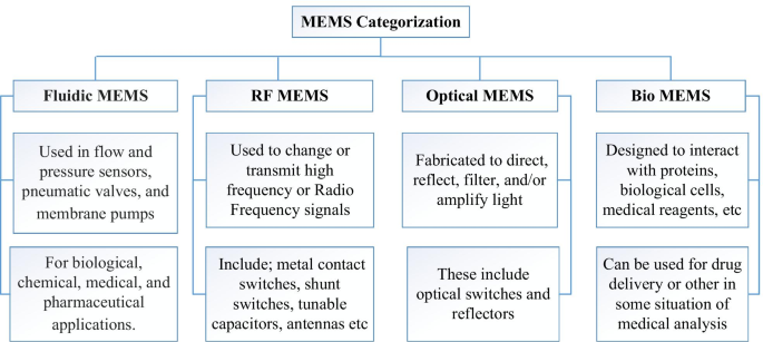
MEMS 장치 분류
현재 기술의 대부분에서 MEMS 센서는 가전 제품에서 항공 산업에 이르기까지 많은 실제 응용 분야에서 선호되는 새로운 분야입니다. MEMS의 가장 중요한 특징은 반도체 칩의 전기 부품과 효과적으로 통신하는 능력이며, 센서 산업은 전자 기능과 기계적 동작을 결합하여 MEMS 기술을 사용하여 혁명을 일으켰습니다[34]. 일반적으로 낮은 전력 소비와 높은 감도로 인해 작은 크기 [35, 36]. MEMS 기반 센서 장치는 다양한 응용 분야에서 중요한 역할을 하는 많은 장점을 가지고 있습니다. 이러한 장점은 어레이 제조 가능성으로 인한 저렴한 비용[37, 38], 낮은 전력 소비[37,38,39,40] 및 작은 크기[38,39,40,41,42]를 포함합니다. 또한 MEMS는 경량, 고해상도, 안정적인 성능 및 다른 장치 및 시스템과의 통합 용이성과 같은 많은 다른 이점을 가지고 있습니다. 관성 센서, 화학 센서, 잉크젯 프린터, 자이로스코프, 위성, RF 통신, 스마트폰, 압력 센서, 가속도계, 생체의학 기기 [43], 군사 응용 프로그램, 운동 및 힘과 같은 여러 영역에서 마이크로 기계에서 마이크로 기계 장치로의 축소가 개선되었습니다. 센서[44]. 게다가, 제조 공정의 저렴한 비용과 단순성은 상업적 제조에서 중요한 역할을 합니다[45].
작동 원리에 따라 센서 장치는 작동 원리에 따라 두 가지 범주로 나눌 수 있습니다. 장치 작동의 정적 및 동적 모드[46, 47]. MEMS 장치가 정적 모드를 기반으로 하는 경우 주파수 신호는 포함되지 않습니다. 또한 표면 흡착 질량으로 인해 빔이 편향되어 응력 및 구조적 변형의 일시적인 결과가 발생합니다. 압저항의 변화로 광학적으로 감지하거나 감지할 수 있습니다. 특정 화학적 결합은 장치 표면에서 발생하며 내부 나노 역학은 MEMS 빔 감지를 구부릴 수 있습니다[46]. 동적 모드에서 장치의 최적 성능을 얻으려면 기계적 공진 주파수를 자극해야 합니다. 진동 시스템이 달성할 수 있고 특정 시스템에서 최대 공진을 발생시킬 수 있는 최대 진폭을 공진 주파수라고 합니다. 공진 주파수가 빔의 스프링 상수와 유효 질량의 두 가지 주요 매개변수에 의해 영향을 받는 경우 이러한 매개변수에 따라 변경됩니다. 이것은 공진 주파수의 변화를 감지 수단으로 활용하기 위한 작동 원리입니다. 원하는 감도와 해상도를 얻으려면 품질 요소가 높아야 합니다[48, 49]. 이러한 메커니즘은 MEMS 기반 장치의 작동 및 출력 신호 감지의 기반이 되기 때문에 이해하고 비교할 필요가 있습니다.
작동 기술은 입력 에너지를 미세 구조 운동으로 변환하는 메커니즘에 주어진 용어입니다. MEMS 장치를 작동시키는 다양한 원리와 접근 방식이 있으며[7, 50,51,52,53,54,55], 그 중 가장 중요한 것은 다음과 같습니다. 정전기 작동[56,57,58,59,60,61,62, 63,64], 전열 작동 [4, 44, 65,66,67,68], 전자기 작동 [7, 69] 및 압전 작동 [48, 70] (그림 2). 보완 금속 산화물 반도체 CMOS-MEMS 센서 장치는 평행판 커패시터를 사용한 정전기 작동 또는 마이크로히터를 사용한 전열 작동으로 작동하도록 설계되었습니다. 반면에 PolyMUMP 및 MetalMUMPs 센서 장치는 내장된 마이크로히터를 사용하여 전열 작동을 사용하도록 설계되었습니다[71].
<그림>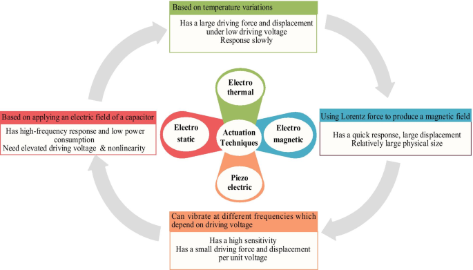
MEMS 기반 센서 장치의 작동 기술
MEMS 기반 장치는 사인파 힘 F을 적용하여 작동될 수 있습니다. (그 ), 앞서 언급한 작동 방법 중 하나를 통해. 식 (1)은 M 이후 일반 운동 방정식을 찾는 데 사용됩니다. 상판의 총 질량, b 감쇠 계수, k 유연한 빔의 스프링 상수,
$$M\ddot{\gamma } + b\dot{\gamma } + k\gamma =F(t)$$ (1)여기서 F z에서 외부 구동력의 진폭을 나타냅니다. -방향, \(\ddot{\gamma }\)\(\ddot{\upgamma }\), \(\dot{\upgamma }\) \(\dot{\gamma }\) 및 γ 는 각각 질량의 가속도, 속도 및 변위입니다.
정전기 액추에이터는 매우 널리 퍼져 있습니다. 그들은 빠른 응답 시간과 낮은 전력 소비를 가지고 있습니다[72]. 반면에 전열 원리를 사용하는 액츄에이터가 인기가 있습니다. 그들은 낮은 구동 전압에서 큰 구동력과 변위를 가지고 있습니다. 전자기 액츄에이터는 빠른 응답, 큰 변위와 같은 몇 가지 장점이 있습니다. 압전 원리를 이용한 액츄에이터는 구동력과 단위 전압당 변위가 작지만 높은 감도를 가지고 있습니다. 따라서 이러한 작동 방식 중 하나를 사용하여 고성능 장치를 얻으려면 발생하는 원리를 잘 이해하는 것이 중요합니다.
정전기 작동의 주요 소스는 커패시터의 전기장이며 반대 전하를 가진 두 평행판 사이의 인력에 의존합니다[12]. 정전기 작동은 고정판과 가동판 사이에서 발생하는 일정한 거리를 가진 두 전하 사이의 역수를 나타내는 쿨롱의 법칙을 기반으로 합니다. 정전기 작동은 MEMS 장치 작동에 가장 널리 사용되는 메커니즘 중 하나로 간주됩니다. 그들은 단순한 디자인, 빠른 응답 시간, 제조 용이성 및 낮은 전력 소비를 가지고 있습니다. 그러나 이러한 유형의 액츄에이터에서는 비선형성과 구동 전압의 상승이 주요 문제이다[72]. 정전기 작동에서 MEMS를 연구할 때 일부 유형의 정전기 작동을 주의 깊게 고려해야 합니다. 가장 널리 퍼진 형태는 두 개의 단순한 평행판으로 구성된 축전기 또는 여러 개의 맞물리거나 맞물리지 않은 핑거로 구성된 빗살 구동 구조를 기반으로 합니다[72, 73]. 기존의 방법[74]은 상부 이동 플레이트가 특정 극성을 갖고 하부 고정 플레이트가 반대 극성을 갖는 평행 플레이트 작동이다(Fig. 3). 움직이는 판의 변위와 진동은 두 판 사이의 전압 차이에 따라 달라집니다. 전하의 극성이 같으면 고정판과 이동판 사이에 반발 변위가 발생하지만 두 판이 서로 다른 전하를 띠면 이동판이 고정판에 끌립니다. 이동판의 전하 종류가 주기적으로 바뀔 때 발동되는 결과[50, 56, 74]
<그림>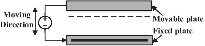
정전기 작동을 위한 병렬 플레이트 커패시터 [75]
인입 불안정성은 고정판이 마이크로빔 바로 아래에 있고 정적 마찰로 인해 장치가 붕괴되기 때문에 평행판을 정전기적으로 구동할 때 주요 문제 중 하나입니다[74, 76]. 콤 드라이브 액추에이터는 맞물린 핑거 구조의 2개의 콤 세트로 구성됩니다(그림 4). 그들은 일반적으로 하나의 빗 핑거가 고정되는 기판에 대해 동일한 평행 플레이트에 배치되고 다른 하나는 고정 플레이트를 향해 또는 고정 플레이트에서 멀어지도록 이동하기 위해 유연한 구조(예:스프링)에 연결됩니다[72]. 가동 콤과 고정 콤 핑거 사이에 다른 전압이 인가되면 프린지 필드의 정전기력이 고정된 외부 사인파 힘에 의해 두 콤을 함께 끌어당깁니다. 일반적으로 평행 플레이트 커패시터는 액추에이터의 고정 플레이트와 이동 플레이트 사이에 더 큰 오버랩 커패시턴스가 있기 때문에 단위 면적당 빗살 구동 액추에이터보다 강합니다. 그러나 설계자는 다음 두 가지 주요 이유로 인해 콤 액추에이터를 선호합니다. 즉, 더 큰 변위를 생성하고(수십 마이크로미터 사용 가능) 힘은 상대적으로 변위와 관련이 없습니다. 전반적으로 정전기 작동은 마이크로 기계식 액추에이터[77], 바이오센서 애플리케이션[56], 습도 감지[57], 입자 및 질량 감지 애플리케이션[50, 78], MEMS 나노포지셔닝 시스템[58], RF MEMS 스위치 애플리케이션[ 13, 79], MEMS 오실레이터의 폐루프 노이즈[60], 내비게이션(자동차 GPS)[62, 80], 자이로스코프[81], 호기의 바이오마커 감지[82] 및 질량 감지 가스 센서[ 63]. 게다가, 당뇨병의 비침습적 스크리닝을 위한 정전식 및 용량성 CMOS-MEMS 기반 센서 장치의 이론적 모델도 보고되었습니다. 호기(EB)에서 아세톤 증기 검출을 통해 당뇨병 스크리닝을 수행하였고, 여기서 키토산 폴리머를 센싱 물질로 사용하였다. 구체적으로 최적화된 감도는 약 0.042, 0.066, 0.13, 0.18 및 0.26pm/ppm으로 보고되었습니다[83].
<그림>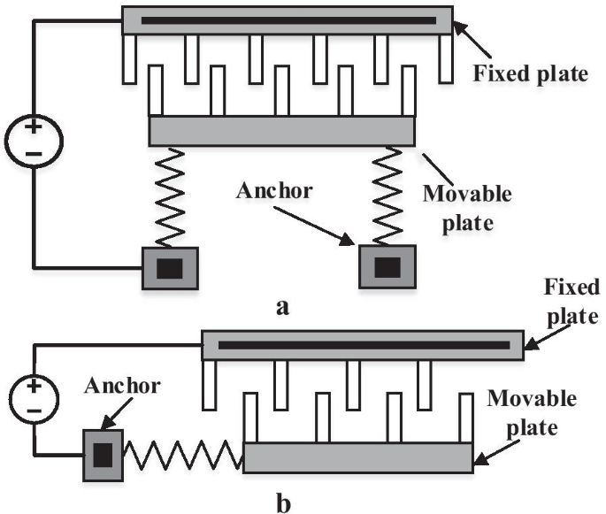
정전기 콤 드라이브 구성의 개략도 [84, 85], a 세로로 맞물린 빗형 액추에이터; ㄴ 가로 액추에이터
MEMS 장치를 공진 상태 또는 진동 모드로 여기하려면 고정자와 회전자의 두 판 사이에 AC 전압을 인가하여 대체 구동을 수행해야 합니다. 표준 운전 모드는 다음 [49]에 따라 표시됩니다. 단순 대체 전압(V 1 죄ωt) , dc 바이어스가 있는 교류 전압(V 0 + V 1 죄ωt) 푸시-풀 구동(그림 5). 푸시-풀 구동은 로터의 양쪽에 구조적 힘이 가해질 수 있기 때문에 일반적으로 최상의 솔루션으로 간주됩니다. 푸시-풀은 콤 드라이브 방식에 적합한 이상적인 드라이브입니다[49].
<그림>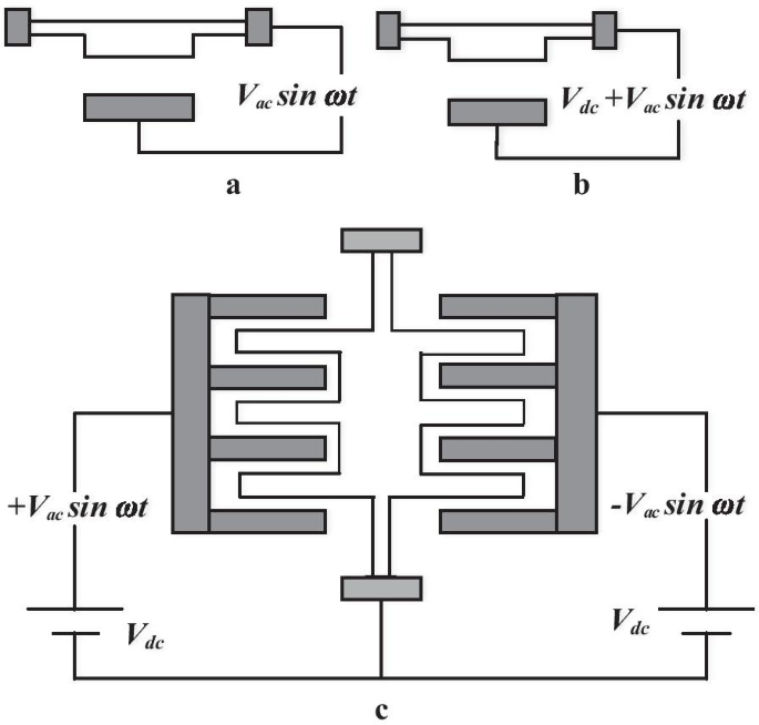
빗살형 공진기 a 간단한 대체 전압 구동, b DC 바이어스가 있는 교류 전압 및 c 푸시-풀 구동 방식 [86]
전열 기술은 MEMS 드라이브에서 주로 활용되는 반면 센싱 애플리케이션에서는 거의 활용되지 않습니다[72]. 전열 기술은 본질적으로 원하는 변위로 움직임을 생성하는 유연한 구성에 적합합니다. 구동은 서로 다른 층의 온도차에 대한 응답으로 발생하는 열력으로 인해 내장된 마이크로히터의 단자를 통해 인가된 AC 전류에 의해 전도됩니다[66]. 마이크로 히터는 다양한 재료 층의 구성 요소로 만들어지며 높은 온도에서 작동합니다. AC 전류가 인가되면 장치의 온도가 상승합니다. 서로 다른 재료의 열팽창 계수(CTE)의 불일치로 인해 재료가 팽창하여 장치가 구부러지는 열 응력을 유발합니다[72]. 반면에 냉각 방식은 기판으로의 전도와 주변 공기(또는 액체)로의 대류를 통해 접근할 수 있습니다.
이러한 온도 변화는 [44, 87]에 보고된 바와 같이 (1) 장치의 치수 변화 또는 장치 내부에서 발생하는 응력, (2) 온도에 따라 장치의 재료 특성이 변하는 두 가지 방식으로 장치에 영향을 미칩니다. 현재 기술은 마이크로히터에 압축될 필요가 있습니다. Microheater는 저항에 특정 전류를 인가하여 원하는 열을 발생시켜 낮은 전력 손실과 빠른 응답 시간을 초래할 수 있습니다. 전열력은 (2) [88]로 설명할 수 있습니다.
$$F_{th} =\alpha_{T} AE(T - T_{0} )$$ (2)여기서 α T CTE, E 빔의 영률, A 는 빔의 단면적, T 는 최종 온도이며 T 0 는 가열 전의 초기 온도입니다. 마이크로히터 설계에는 여러 재료가 사용되었습니다. 예를 들어, 최고의 성능, 정확도, 광범위한 온도 범위 및 안정성을 달성하려면 백금과 금이 마이크로히터에 대한 최상의 결정이 될 것입니다[89]. 그러나 비용이 많이 듭니다[90]. MEMS 센서에서 마이크로히터를 활용하려면 생성된 열을 유용한 출력으로 변환하기 위해 내장된 온도 센서가 필요합니다. 온도 센서의 경우 백금은 − 200ºC ~ 800ºC 온도 범위에서 사용할 수 있고 니켈은 − 100 ~ 260ºC에서 사용할 수 있습니다[90]. 보고서에 따르면 알루미늄은 온도 감지에 좋은 재료이기도 합니다[91]. 그림 6은 U-빔 액츄에이터(핫/콜드 암), 바이모프 액츄에이터(이중 재료 액츄에이터) 및 버클링 액츄에이터(V-빔 액츄에이터 또는 셔틀 빔)를 포함하는 전열 작동의 일반적인 메커니즘을 보여줍니다.
<그림>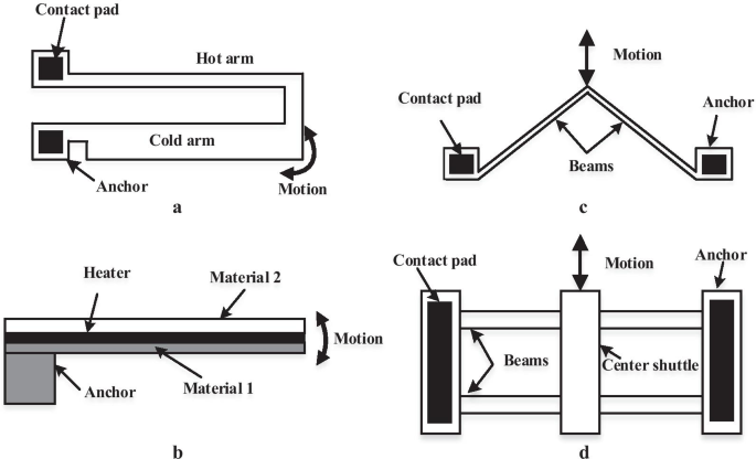
전열 작동의 개략도 a U-빔 액추에이터(핫/콜드 암), b 바이모프 액츄에이터(Bi-Material Actuator), c 그리고 d 버클링 액추에이터(V-빔 액추에이터 및 셔틀 빔) [67, 92]
U-빔 액추에이터는 핫/콜드 암으로도 알려져 있으며, 액추에이터는 좁은 암(핫), 넓은 암(콜드) 앵커 및 접촉 패드로 구성됩니다[67, 92]. 주로 기판과 비교하여 면내 또는 수평가동에 사용됩니다. 이 기술의 작동 원리는 접촉 패드에 차동 전압을 적용하는 데 의존하고, 전류는 암을 통해 흐르고, 핫 암(높은 저항)은 콜드 암(낮은 저항)보다 더 많은 전류 밀도를 가열합니다. 따라서 폭이 좁은 핫 암은 더 뜨겁고 두꺼운 암보다 더 많이 팽창합니다. 뜨거운 암은 큰 열 응력을 생성합니다. 양쪽 팔 사이의 이러한 차등 변형으로 인해 전체 장치가 편향됩니다.
이중 재료라고도 하는 바이모프 액추에이터는 서로 결합된 두 개의 서로 다른 열팽창 재료로 구성됩니다. 처음 두 액츄에이터와 달리 바이모프 액츄에이터[93]는 일반적으로 평면 외 작동에 사용됩니다. 전류가 빔을 통과함에 따라 재료의 온도가 증가합니다. 이 온도는 열팽창 계수가 다르기 때문에 한 재료에서 다른 재료보다 더 큰 팽창을 일으켜 열 응력과 장치의 굽힘을 초래합니다.
열 좌굴 액추에이터는 V-빔 또는 셔틀 빔[94], 앵커 및 접촉 패드로 구성되며, 이는 평면 내 또는 측면 작동에도 주로 사용됩니다. 빔 사이에 전류가 흐르면서 빔 온도 상승은 발생하는 줄 가열로 인해 열 팽창을 일으키며, 이는 팽창하여 셔틀을 이동시키거나 장치의 중심 빔을 가장 단순하고 저항이 적은 방향으로 앞으로 밀어내는 경향이 있습니다.
실제 구현에서 열적으로 작동하는 대부분의 MEMS 장치는 고유 진동수에 가까운 주파수에서 진동하므로 장치의 고유 진동수를 계산하는 것이 필수적입니다. 전열 기술은 매우 낮은 여기 전압에서 토우 층 재료의 열 팽창을 기반으로 하는 큰 추진력과 변위로 인해 더욱 널리 보급되었으며, 이는 유사한 측정이 사용될 때 다른 전략으로 달성할 수 없습니다[85, 95]. 전열 작동은 큰 변위[95], 제작의 용이성[72], 큰 힘 및 상대적으로 낮은 인가 전압[52]과 같은 여러 이점을 나타냅니다. 반대로 많은 양의 전류와 저전압 증폭기가 필요합니다. 또한 줄 가열로 인해 높은 전력을 소비합니다. 또 다른 제한 사항은 주변 온도에 대한 민감도입니다. 마지막으로, 전열 작동으로 인해 증가된 여기 온도와 열은 시스템의 패키징 단계와 함께 인접 전자 장치에 몇 가지 단점을 유발할 수 있습니다[72].
수많은 유형의 전열 작동이 개발되고 연구되었습니다. 핫/콜드 암 [96,97,98], 이중 재료 또는 바이모프 [98, 99] 및 열 좌굴 액추에이터 [98, 100]. 참고 문헌 [101]은 바이모프 액츄에이터를 사용하여 열 작동 하에서 마이크로 캔틸레버 진동을 조사했습니다. 참고 문헌 [102]은 MUMP 공정을 사용하여 제작된 폴리실리콘 마이크로 링 열 작동(RTA)을 위한 구조화된 절차를 제안했습니다. 열 작동을 기반으로 하는 마이크로 캔틸레버가 설계되었습니다. 그들은 시스템이 진공 또는 유체(기체) 액체에 있다고 가정하고 분석 솔루션을 제안했습니다[103]. Dennis et al. [44] 이산화티타늄(TiO2)을 사용하여 습도 수준을 측정하기 위해 비교적 높은 온도(40–80 °C)에서 작동하는 마이크로히터가 내장된 (CMOS-MEMS) 시스템을 제작했습니다. ) 나노 입자를 감지 물질로 사용합니다. 센서는 Wheatstone 브리지 회로에 연결된 PZR(압전 저항) 센서를 사용하여 평가된 전열 작동 및 출력 신호를 사용하여 동적 모드에서 작동되었습니다. 습도 센서 출력 전압은 습도가 35% RH에서 95% RH로 증가함에 따라 0.585에서 30.580 mV로 상승합니다. The sensitivity of the humidity sensor increases linearly from 0.102 mV/% RH to 0.501 mV/% RH with an increase in the temperature from 40 to 80 °C and a maximum hysteresis of 0.87% RH is found at a relative humidity of 80%. In a further notable contribution, Almur et al. [104] modelled a MetalMUMPs acetone vapour sensing system based on electrothermal actuation and capacitive sensing. The output voltage change was found to increase linearly with increasing the acetone vapor concentration from 100 to 500 ppm with a concentration sensitivity of 0.65 mV/ppm. Due to the thick nickel layer of the MetalMUMPs technology used the device has very high mass (4.7 × 10 –8 kg) and low mass sensitivity (0.118 MHz/pg).
The electromagnetic operation has long been utilized in the sensing and driving of the large scaling applications (such as loudspeakers). This technique demands electricity to stimulate the magnetic effect. It uses the electromagnetic force (also can be called Lorentz force after the Dutch physicist Hendrik A. Lorentz 1895) to produce a magnetic field to the resonator by applying an alternating current on the coil or inductor integrated into the resonator (Fig. 7). Lorentz Force is defined as the force generated on a point charge as a result of the combined electric and magnetic forces on the charge [72]. Electromagnetic actuation has also been utilized as a guide to other actuation techniques, for example, electrostatic [33] and electrothermal [34]. In this technique, when a conductor conveying an electric current I can be applied to an external magnetic field B , this will induce a Lorentz force F 엘 as stated by (3) [72].
$$\vec{F}_{L} =L\vec{I} \times \vec{B}$$ (3)여기서 L indicted to the conductor length and × refers to the cross product operation. The current in the conductive element located within the magnetic field generates an electromagnetic force in a direction perpendicular to the current and the magnetic field. This force has a directly proportional to the current, magnetic flux density and length of the microbeam. Because of the interaction generated by the current between the magnet and the magnetic field, a mechanical displacement on the microbeam will be generated as a result of the applied current to the micro-coil. For example, electromagnetic actuation has been used to stimulate microbeam when being exposed to an external magnetic field by flowing current through the microbeam, as seen in Fig. 7a. Similarly, as alternating current flows through the device on the microbeam, this approach can be used to excite the out-of-plane resonator (Fig. 7b). Lorentz forces of equal value and opposite directions are produced if the coil is deposited on a structure of the microbeam. The opposite directions of the current flowing through the different parts of the coil correspond to these forces. Such forces balance one another out. Figure 7c, however, can induce a net motion that is used to actuate the microbeam [72].

Schematic of the electromagnetic actuation using Lorentz forces a in-plane actuator, b 및 c out-of-plane actuator [72]
The electromagnetic technique involves many merits over the other kind of actuation techniques. The main advantages of the electromagnetic actuation include the large displacement without the influence of the nonlinear effect [105], lower voltages due to they based on current rather than voltage-driven [7], in addition, they have a high reproducibility rate, they also have more features like rapid response, high accuracy, and the merit for controlling easily. For MEMS applications, the electromagnetic technique is the best choice to achieve maximum driving force for device size ratio [106]. However, they still suffering from some drawbacks due to using the huge current resulting in high power consumption, also their fabrication is complicated (normally be in need of inductive parts to produce magnetic flux also the possibility of including the manufacture of coils, and the deposition of a magnetic material) [7]. This fact combined with constructive difficulties has limited magnetic actuation applications. However, there are successful application examples in the literature as it may exist in MEMS switches devices [7], Optical switches, and micro scanners [69], gyroscopes [107], or relays [108]. Many researches are also based on magnetic actuation [109]. The magnetic microsensors utilizing the commercial 0.35 μm CMOS process has been investigated [110]. In a further contribution, Barba et al. [111] designed an electromagnetically actuated MEMS cantilevers proposed in order to minimize parasitic phenomena using Boron-doped silicon. In another seminal work, an electromagnetic and Piezoelectric actuated and piezoresistive sensed CMOS- MEMS device has been modelled for humidity sensing using ZnO NRs (6 μm/chitosan SAMs) as a sensing material [83]. The sensitivity was found to be 83.3 ppm [112].
Piezoelectric effect indicates the capability of a particular material to produce an electrical voltage in response to applied the mechanical stress. Piezoelectricity was discovered by the Curie brothers in 1880, and 'Piezo' meaning is coming from the Greek word that is mean 'press' or 'push'. A piezoelectric actuator defined as transducers that converts an applied potential into a mechanical movement or strain based on the piezoelectric influence [72]. Piezoelectric materials like quartz, zinc oxide, lead zirconate titanate (piezoelectric ceramic material PZT), and polyvinylidene difluoride (PVDF) are commonly used in sensor and actuator applications on a macro scale as well as in MEMS applications in recent years, but the sensing is limited due to their lack of a DC response [49]. Piezoelectric materials act electrically as insulators and required to be placed between two conductive electrodes so as to gather charge or to apply an electric-field (using an interdigitated electrode or sandwich structure) [113].
In MEMS devices, the basic principle of the piezoelectric actuation method is based on using a thin piezoelectric layer that is deposited as a part of the MEMS beam between flexible (Fig. 8). When a voltage is applied to the piezoelectric layer, the piezoelectric material expands according to the polarization of the applied voltage, which causes an axial bending across the length of the flexible beam [114].

Schematic of the piezoelectric actuator [72]
In general, piezoelectric actuators exhibit a lot of advantages such as high output force, good operating bandwidth, very compact size, lightweight, low power consumption, and fast response [114, 115]. Their characteristics are well known and have been used for decades. Most first sensors use piezoelectric actuation and are still in use today. However, small displacements of actuators are a major drawback, and their high-temperature sensitivity [72], nonlinear working area and hysteresis limit their wide range of applications [49]. Piezoelectric materials are very brittle. They can seldom be utilized alone but are often connected to a flexible structure for actuation and sensing applications. There are several works based on piezoelectric actuation [2, 48, 114, 116] studied the prospective to use a piezoresistive microcantilever for environment application, particularly for humidity sensing. Mahdavi et al. [117] proposed a new class of accurate dew point measurements taking advantage of thin-film Piezoelectric-on-Silicon (TPoS) resonators using ZnO NRs (6 μm/chitosan SAMs). The sensitivity was found to be 16.9–83.3 ppm at the range of response time of 46 s/167 s. sensitivity to mass loading based on piezoelectric excitation is investigated for chemical sensing [118, 119] reported piezoelectric transduction of flexural-mode silicon resonators to achieve efficient temperature compensation. The resonance gas sensor using piezoelectric MEMS for defence applications was reported [120].
Different types of MEMS actuators require different drive electronics. As per mentioned in this article, there are different principles and approaches to actuate MEMS devices. The most important of which include:electrostatic actuation, electrothermal actuation, electromagnetic actuation, and piezoelectric actuation. Electrostatic actuators are a traditional field and considered one of the most popular mechanisms for actuating MEMS devices. They have a simple design, fast response time, ease of fabrication and low power consumption. However, the non-linearity and the elevated value of the driving voltage is the major matter of this type of actuator. Electrothermal actuators provide very low resistance to their drive sources and require high currents rather than high voltages to move them. High voltage amplifiers are not particularly suitable for use in electrothermal MEMS actuators. Instead, a low voltage and high current signal source are required. Of course, this can also work if the output current of the high voltage amplifier is large enough to drive the electrothermal actuator, but it is not a particularly energy-efficient or cost-effective solution. For MEMS applications, electromagnetic technology is the best choice to achieve maximum driving force per device size ratio. However, they still suffering from some drawbacks due to using the huge current that results in high power consumption, also their fabrication is complicated (normally be in need of inductive parts to produce magnetic flux also the possibility of including the manufacture of coils, and the deposition of a magnetic material). Piezoelectric actuators also required high voltage amplifiers, but since they are typically used for resonance, the drive requirements in terms of driving voltage are typically lower than those required for other actuators. The recent research of MEMS-based sensor devices which can be actuated using the four basic actuation techniques that have been used during the last few years for many applications, as shown in Table 2. It can be clearly observed that there is a rising development pattern in the field of micro-assembly and micromanipulation for MEMS-based sensor devices that have been categorized based on actuation techniques. Nowadays, a wide range of applications has been identified for MEMS-based sensor devices that provide high sensitivity and resolution. The sensing systems are getting more robust and reliable due to the integration configuration.
The sensing mechanism is used to sense the output of the MEMS devices. The basic of the sensing technique is based on the use of a polymer deposited on the sensing layer of the device to absorb a particular chemical that creates a variation in the stress, mass, electrical or mechanical characteristics of the beam. To estimate the change in the mass, the resonant frequency of the device can be measured based on the detected mass increment that is one of its parameters. Then again, when the polymer absorbs the mass, piezoresistor that is situated on the surface of the sensing element can be used to estimate the mass of the beam. Another method of detecting suspected chemicals is to use thermocouples to measure temperature changes caused by the heat generated by the polymer absorbing analyte [49].
To sense the output of these MEMS devices methods such as piezoresistive, capacitive or optical mechanisms are used (Fig. 9) [123]. Different sensing mechanisms have different advantages and disadvantages at the same time.

Sensing mechanisms of MEMS-based sensor devices
For instance, optical sensing has good feasibility; however, it is very expensive to implement compared to capacitive and piezoresistive techniques [124]. Capacitive and piezoresistive techniques are the common methods used to sense the output signal. CMOS- MEMS device was designed to encompass both piezoresistive and capacitive sensing techniques due to the features of 0.35 µm CMOS technology used to design it. In contrast, PolyMUMPs and MetalMUMPs devices were designed to use only capacitive sensing techniques.
Piezoresistive is a common sensing principle used in MEMS devices. Essentially, the principle of piezoresistive materials is based on the resistance change when their strain changes in response to applied stress. This change can be observed in the electrical resistance of the material of the device as a consequence of a surface-stress change due to bending. The resistance value of the piezoresistor with the resistivity ρ of a resistor, length of l and cross-section area A is given by (4) [29].
$$R =\frac{\rho l}{A}$$ (4)The change ΔR in resistance is proportional to the applied strain can be defined in (5) [29, 125].
$$\Delta R =G\varepsilon R$$ (5)where G is the gauge factor work as a proportionality constant of the piezoresistor, ε is the strain in the material, and R is the piezoresistor resistance. A piezoresistive element behaves differently towards longitudinal and transverse strain component presented by [29]. According to (5), the resistance of a piezoresistor can vary owing to the changes of the geometry (length and cross-section) or in the property of the material (resistivity). Piezoresistive detection depends on the difference in resistivity of material when stress is applied. In a piezoresistive material, the change of resistivity because of the application of stress has a much greater effect on the resistance than the change in resistivity because of a change in the geometry (sensors rely on the change of resistance owing to the geometry are so-called strain gauges) [72]. (Fig. 10) shows different resistor orientations and external force loading directions [88].

아 Longitudinal piezoresistance dominates, b 및 c transverse piezoresistance dominates presented [29]
The main drawback of this sensing mechanism is the solid temperature reliance of resistivity. To limit this impact, normally, a collecting of four piezoresistive designed is utilized to shape a Wheatstone bridge. This limits the temperature reliance [72]. Furthermore, the small changes in the electric signal generated from gauges are translated and gauged as voltages utilizing this Wheatstone bridge [49]. Wheatstone bridge utilizes four resistors arranged in the bridge of the four arms (Fig. 11). Based on the quantity of these active resistors (acting as a transducer), single active bridge (single transducer), half active bridge (double transducers), and the full active bridge (quadruple transducers) of the bridge of Wheatstone might be utilized as reported [72]. The single active bridge as well called Quarter Bridge that utilizes just a single active component which changes because of a physical ambient, for example, pressure, power, temperature, while the remnants of that resistors will be passive and so on. MEMS systems have been used as temperature, calorimeter, and in combination with the Wheatstone bridge, sensors allow the base fluctuations. Thermal bridge system is one of the best-known sensing platforms among MEMS. In the AC-driven Wheatstone bridge configuration (Fig. 11b), researchers have utilized the resistance-based thermometry to analyse temperature changes with micro-Kelvin resolution. In an overview, the right half of the bridge comprises a sensing resistor on the lower branch with associated resistance on the top, while the left side is defined as the matching one. Fixed resistors with a relatively low resistance coefficient of temperature are used with resistance values, which was chosen to enhance stability and resolution based on the previous study [126].

Schematic types of a Wheatstone bridge, a quarter bridge, b half-bridge, and c full-bridge configurations [72]
Silicon piezoresistor and polysilicon patches are generally utilized in MEMS sensors. The resistivity of silicon relies upon its strategy for doping. N-type doped with silicon is less sensitive than p-type. This raises limitation to the fabrications. In this situation, an in-plane transversal and in-plane longitudinal will be the most significant elements [72]. For semiconductor materials like silicon, the longitudinal and transverse gauge factors owing to geometry change are quite tiny compared to their values due to resistivity change, hereafter the change in geometry can be ignored, and the longitudinal and transverse gauge factors due to only the resistivity change are found using (6) and (7), respectively [127].
$$G_{L} =\pi_{L} E$$ (6) $$G_{T} =\pi_{T} E$$ (7)여기서 E is Young's modulus of the piezoresistive material. π L and π T are the longitudinal and transverse piezoresistance coefficients, respectively, for arbitrarily oriented polysilicon grains, and their values are given in Table 3 [19].
Currently, the piezoresistive effect has been utilized as a bio-or chemical detection [48], humidity sensing purpose [4], switch applications [59], biomarker detection in exhaled breath [82], micro scanners [69], pressure sensing [128], and mass-sensitive gas sensors [63]. Zope et al. [117] developed a resistively sensed thermally-driven piezo resonator composed predominantly of CMOS material for mass sensing applications. whereas mass sensitivity of 24.96 kHz/ng was reported. The extracted mass resolution of 16.3 fg have also been observed, hence showing great potential to serve as an aerosol sensor).
The capacitive sensing mechanism is based on measuring the changes of the capacitance between the stator and rotor fingers or between the fixed plate and movable plate [88]. Capacitive sensing is the main dominant method for micromachined applications due to its compatibility with all the fabrication approaches and stiffness [129, 130]. Capacitive sensing has many attractive features include high sensitivity, low power consumption, simplicity in design, low drift and low-temperature dependency. Furthermore, the measurement of the output signal can be easily fabricated on the PolyMUMPs die using capacitive sensing. Only a single parallel plate can be used to capacitively sensed the variations in the natural frequency or amplitude of the MEMS devices (such as a CMOS-MEMS device and a PolyMUMPs device) or by applying a comb finger (such as a MetalMUMPs device).
For CMOS-MEMS device and PolyMUMPs devices, when there is no actuation (Fig. 12a), the initial static sensed capacitance (Cs0 ) between the lower fixed plate and the movable top plate is calculated using (8) [19].
$$C_{s0} =\frac{{\varepsilon A_{s} }}{{z_{0} }}$$ (8)where ℇ is the relative permittivity of the dielectrics, As is the area of the sensed plates and z0 is the gap between the fixed and movable plates. When the movable plate is displaced by z (Fig. 12b) the initial gap changes, and hence the capacitance will change too, and it is found by (9).
$$C_{s} (z) =\frac{{\varepsilon A_{s} }}{{z_{0} - z}} =C_{s0} \frac{{z_{0} }}{{z_{0} - z}}$$ (9)
Parallel plate capacitor showing a initial condition and b after displacing the movable plate [19]
At the same time, for the MetalMUMPs devices, the output can be detected capacitively by utilizing the differential comb fingers design. As appeared in Fig. 13, there are two arrangements of fixed comb fingers to have the differential capacitance.

Comb fingers configuration for MetalMUMPs device showing a the initial condition and b the displacement of the vibrating comb finger [19]
For the initial condition, when the device is not actuated (Fig. 13a), the static detected capacitance C0 for every set of vibrating-fixed fingers could be calculated by (10).
$$C_{0} =n\frac{{\varepsilon l_{f} w_{f} }}{d}$$ (10)where l f and w f are length and width of the overlapping area of the vibrating and fixed comb fingers, respectively. d is the gap between the fixed and vibrating comb fingers and n is the number of the vibrating comb fingers. When the device is moved by y toward the fixed comb finger one as appeared by (Fig. 13b), the capacitances C 1 및 C 2 will be changed and relying upon that shift, and their values can be calculated using (11) and (12), respectively.
$$C_{1} (x) =n\frac{{\varepsilon l_{f} w}}{d - y}$$ (11) $$C_{2} (x) =n\frac{{\varepsilon l_{f} w}}{d + y}$$ (12)The output signal of the device will be measured as a voltage due to change in the sensing capacitance upon actuation using MS3110 capacitive readout circuit that translates the change in capacitance to the output voltage change in response to the temperature of the microheaters. Nowadays, capacitive effects are used in MEMS resonators [60], biosensor application [56], humidity sensor [57], diabetes screening [66], Navigation (automobile Global Positioning System (GPS)) [62], a low noise accelerometer [131], and RF MEMS capacitive switches [132].
Optical sensing mechanism depends on detecting the changes in the transmitted light compared to the received light. The detection of compound species by spectral transmission strategy is broadly acknowledged. Optical sensors are notable due to their selectivity since it does not rely upon any chemical reaction or any chemical catalyst activities. Air pollutants identification is recognized by using the characteristics of the optical species (for example, absorption, refractive index, Raman scattering, fluorescence, and reflection). Optical sensors utilize emission and absorption measurements primarily through different technologies such as Fourier transform infrared spectroscopy (FTIR), surface plasma resonance (SPR), differential optical absorption spectroscopy (DOAS), laser diode absorption spectroscopy (LDAS), cavity ring-down spectroscopy (CRDS), non-dispersive infrared (NDIR) spectroscopy, light detection and ranging (LIDAR), UV fluorescence and chemiluminescence for the sensing of air pollutants in air specimens. Normally, the light will be cross through, modified or reflected by some space having the relevant medium (Fig. 14). Beer–Lambert law can be used to govern the optical detection of the air pollutants as per the following:
$$I =I_{0} *e^{ - \alpha l}$$ (13)where the transmitted light through the specimen is I , 나 0 is the received light, α represent the absorptivity, l represents the length of the path.

Schematic representation of an optical MEMS sensor [133]
However, the majority of the applications for optical MEMS are in communications; there are various uses in different fields [134]. The literature covered numerous attempts to introduce the optical detection of air pollutants. A few of these sensors are used to recognize chemicals. This displays the multifunctional part of these sensors. Infrared spectrometry is a case of a technique that can be utilized for optical sensing [135]. In a further notable contribution, Huang and co-workers have also demonstrated [136] the simulation of an integrated optical MEMS accelerometer. The effective simulation results have demonstrated as follows:a resonance frequency of 562.85 Hz, a mechanical sensitivity of 781.64 nm/g, an optical system sensitivity of 1.23, a resolution of 1.037 µg, and low cross-sensitivity. The proposed accelerometer can be used for improvements in MEMS inertial navigation devices. Another model is the Fabry–Perot optical sensor [137]. Basically stated, the principles of this sensor are based on bringing gas into a chamber and a short time later going light through the chamber. Due to changes in the substance piece, the light experiencing will be not exactly equivalent to without the gas. This light is broke down, and from the results, confirmation can be made about the sort of gas being tested. The fruitful testing of an optical MEMS sensor for the location of catechol was reported [133]. The absorbance measurement of catechol oxidation was performed by blue light (472 nm) attached through a MEMS device. The light was transmitted from a free-space blue laser working in persistent wave mode and is focused on a multimode fibre utilizing manually arranged to organize. Received light was coupled by means of the optical fibre to a USB connected spectrophotometer which assisted computerized information collection utilizing the software.
In view of different working principles, the above-mentioned sensing mechanisms can be divided into three types, namely piezoresistive, capacitive and optical mechanisms. There are benefits and drawbacks for different sensing mechanisms at the same time. For instance, optical sensing has good feasibility; however, it is very expensive to implement compared to capacitive and piezoresistive techniques. As a result, piezoresistive and capacitive techniques are the common methods used to sense the output signal. Any small change in the stress could be detected using a piezoresistive technique. A main disadvantage of the piezoresistive sensing technique is the high-temperature reliance of resistivity. In Table 3, present the recent work and progress (last 5 years), including actuation and sensing mechanisms, sensing materials, fabrication technology and application. The miniaturized microchip presented (in Table 4) can be utilized for gas and humidity sensing, human health screening, inertial navigation with good repeatability, high resolution, high sensitivity, and rapid response. In addition, MEMS sensors have been proven to be an effective medium for sensors combined with on-chip electronic circuitry. It can therefore function not only as a portable sensor chip but can also be linked as part of the Internet of Things (IoT) network to achieve real-time and remote high-sensitivity moisture tracking.
Recent developments are about new technologies that can harvest energy from the environment, because sustainable self-sufficient micro/nano power sources are an emerging field of nanoenergy, which involves nanomaterials and nanotechnology when harvesting energy for powering micro/nano systems [139]. The triboelectric charge is produced only on the surface dependent on the physical friction between two separate materials. The triboelectric nanogenerator (TENG) is a device that transforms mechanical energy into contact separation or relative sliding between two materials with opposite polarities. TENG based on the coupling effect between triboelectricity and electrostatic induction in which it’s updated progress and potential applications as new energy technology and as self-powered active sensors. The suggested approach uses biomechanical energy transfer to electricity from human activity [139, 140]. Amongst them is a successful study has been investigated for the conversion to wearable energy from portable biometric devices and self-powered sensors based on triboelectricity (i.e. the charge produced on the touch surface) [141,142,143,144].
To decrease power consumption during operation, sensors of woken up or almost zero-power supplement need to proposed and investigated, meaning that these sensors do not have any energy consumption. With these components of MEMS, MEMS sensors can work for a long period or can be operated in a self-powered.
<리>Looking forward to the future-oriented sensors, sensors with flexibility have become hot topics of the recent research in the latest years owing to their versatility and great prospective in health/human beings applications. Flexible sensors are often used in combination with wearable sensors to have their unique advantages. More than just utilizing the flexible sensor such as a wearable electronic for observation functions, they can be even utilized as a human–machine interface for achieving higher requirements. With the enhancement of the quality of human life, wearable devices and human–machine interfaces have been recognized as important directions for developing sensors of the future with sufficient flexibility and versatile sensing capabilities. Wearable electronic devices can be simply integrated with the human body to extend our perception capabilities. Sensor functions of wearable electronic devices include, but are not limited to, force, strain, electrophysiology, heart rate monitors, temperature, fitness trackers, etc. With the service of various devices among different anatomical positions, development of many applications of the human body sensor can be facilitated from hospital care to fitness and wellness tracking, human–machine interfaces and recognition and assessment of cognitive states.
<리>Meanwhile, by combining MEMS sensor with artificial intelligence (AI), the next generation of sensors will provide clear evolutionary impact and help humans interact with other things in various applications circumstances. Moreover, the quick improvement of the modern community has observed the expanding association among people with machines, demanding huge intelligent human–machine devices. Around a huge data and hypersensitive detecting, MEMS sensor utilizing a machine learning strategy dramatically stimulates the enlargement of the coming generation smart sensing system. This interactive system with next-generation sensor provides consumers with a more comprehensive experience. It can be used for many practical applications, such as simulation of sports training, entertainment, medical rehabilitation and so on.
It is well recognized that MEMS-based sensors play a key role in the field of miniaturization and electronic microcircuits. It is necessary to understand and compare these mechanisms since they are the basis of the MEMS-based devices operation and output signal detection. This article reviews several popular actuation and sensing mechanisms related to MEMS devices that have emerged over the past few decades. This article introduced a descriptive overview to the advancement of the actuation and sensing mechanisms of the MEMS-based sensor devices. The up-to-date trends and the restrictions while giving a valuable perception into the field of emerging actuation and sensing technologies. A comprehensive discussion was presented, underlining the significance of the actuation and sensing mechanisms, its structure, working principles, classification, fabrication and applications. Proper understanding of the actuating and sensing mechanisms for the MEMS-based sensor devices play a vital role in their selection and effective application in various innovative technologies. In addition, the proper selection of actuating and sensing techniques in MEMS sensors based on the desired application such as sensitivity, resonant frequency, input\output voltage, temperature etc., will lead to fast-commercialization and better product stability.
In order to perform various tasks for different applications such as industry and electronic equipment, different MEMS devices with different structures collaborated with diverse actuation and sensing mechanisms will arise in true-life. Moreover, MEMS devices will not only be used for simple tasks, but also for more jobs that are complex. At the same time, MEMS devices will have greater freedom and can meet the needs of a variety of applications. However, in order to pursue higher accuracy and miniaturization, the complexity of MEMS device design will continue to increase. In addition, MEMS products have a close relationship with the market. It can be predicted that MEMS devices will realize more functions, miniaturization and low cost, which is a huge challenge for other products. Therefore, in the next few years, MEMS fabrication approaches will develop to a higher level to meet market demand. With the advancement of MEMS device fabrication processes, unique hardware makers will seek after shorter fabrication cycles and quicker fabrication speeds.
One of the central areas of the future trend in this area is reliability research and improvement methods. Moreover, new materials and cost-effective of the fabrication techniques will provide important opportunities for development. It has been demonstrated that the design capability is not limited to standard principles and can improve qualitative performance. Despite MEMS advantages, few challenges still exist in the following aspects.
The traditional MOS thin films by MEMS techniques often show poor sensitivity to target gases due to the compact surface structure and low crystallinity.
<리>In recent studies, it have tried to integrate high-performance MOS nanomaterials onto microheaters. Still, it is difficult to control and cast the slurry-based MOS nanomaterials onto the suspending heating area of microheaters. However, the low yield and large device-to-device deviation hamper the sensor fabrication on a large scale.
<리>It is also complicated to improve the adhesion between microheaters and sensing materials to get stable parameters, especially at high temperatures > 350 °C which results in decreased sensing performance and low stability [14, 145].
<리>Fabricating sensing films with high sensitivity using MEMS compatible methods is an urgent goal.
<리>Towards a new era, different challenges can face MEMS-based sensors in terms of power supply and intelligence during the operation, such as the challenges of the flexibility of wearable applications, the friendly interactive capabilities of human–machine interface applications, and analysis of the huge data.
해당 없음.
Microelectromechanical system
Potential hydrogen
Integrated circuits
감지 한계
Multi-user MEMS
Microsystems technology
무선 주파수
상보성 금속 산화물 반도체
The coefficient of thermal expansion
Alternating current
직류
Ring thermal actuation
Polyvinylidene difluoride
Global positioning system
푸리에 변환 적외선 분광기
Surface plasma resonance
Differential optical absorption spectroscopy
Laser diode absorption spectroscopy
Cavity ring down spectroscopy
Non-dispersive infrared
Light detection and ranging
Interdigitated electrodes
Piezoresistive
Electrostatic field sensor
Artificial intelligence
나노물질
진동 센서는 중장비의 진동 측정에 사용되는 압전 소자입니다. 이 장치에는 진동 분석에 도움이 되는 감지 요소가 있습니다. 일상 업무에서 항상 접할 수 있는 장치이기도 합니다. 이 기사에서는 무선 진동 센서, 유형, 용도 및 연결 방법에 대해 설명합니다. 또한 필요에 적합한 진동 센서를 배우고 찾는 데 도움이 될 것입니다! 1. 진동 센서란 무엇입니까? 진동 센서의 다른 이름은 압전 진동 센서입니다. 특히 센서는 시스템의 압력, 가속도 및 진동 변화를 측정하여 작동합니다. 진동 센서 모듈의 도움으로 이러한 무선 센서는 Rasp
게임용 로봇 팔을 어떻게 제어할 수 있는지 궁금하신가요? 아니면 근육 활성화를 어떻게 측정할 수 있을까요? 호기심의 열쇠는 EGM 센서에 있습니다. EGM 또는 근전도 검사는 의학 연구 및 신경근 장애 진단에 매우 중요합니다. 또한 강력한 집적 회로와 마이크로컨트롤러의 발명으로 로봇, 보철 및 기타 제어 응용 분야에서 EMG 센서가 등장했습니다. 그러나 EMG는 여전히 비싸고 많은 엔지니어와 애호가 모두에게 손이 닿지 않습니다. 다행히 다음 프로젝트를 위해 EMG 센서를 구축하는 방법을 알려 드리겠습니다. EMG 센서의 용도는