

나노물질

산업 제조
Spintronics는 대체 다기능, 고속, 저에너지 전자 장치를 개발하는 가장 유망한 기술입니다. 특이한 물리적 특성으로 인해 새로운 2차원(2D) 재료는 새로운 스핀트로닉 장치를 탐색하기 위한 새로운 플랫폼을 제공합니다. 최근 2D 스핀트로닉스는 이론 및 실험 연구 모두에서 큰 발전을 이루었습니다. 여기에서 2D 스핀트로닉스의 진행 상황을 검토했습니다. 마지막으로 이 분야에 대한 현재의 도전과 미래의 기회를 지적했다.
거대 자기저항 효과(GMR)의 발견 및 적용으로 스핀트로닉스는 전자의 스핀 정도 자유도를 정보 캐리어로 사용하여 데이터 저장 및 논리 연산을 달성하는 것을 목표로 하는 매력적인 분야로 빠르게 발전했습니다[1,2,3 ]. 전하를 기반으로 하는 기존의 마이크로 전자 장치와 비교하여 스핀트로닉 장치는 스핀 상태를 전환하는 데 필요한 에너지가 적으므로 작동 속도가 빨라지고 에너지 소비가 낮아집니다. 따라서 스핀트로닉스는 대체 다기능, 고속, 저에너지 전자 소자를 개발하는 가장 유망한 기술입니다. STT-MRAM(spin-transfer-torque magnetoresistive random-access memory)이 상업적으로 생산되었지만 다양한 기술적 문제는 여전히 해결되어야 합니다. 주요 과제로는 스핀 극성 캐리어의 효율적인 생성 및 주입, 스핀의 장거리 전송, 스핀 방향 조작 및 감지가 있습니다[4,5,6].
스핀트로닉스의 붐과 병행하여 2차원(2D) 반 데르 발스(vdW) 재료는 그래핀의 분리 이후 재료 연구의 최전선에 있었습니다[7,8,9]. 벌크 재료와 달리 2D vdW 재료는 많은 새로운 물리적 현상을 나타냅니다. 일부 2D 재료는 이미 차세대 2D 스핀트로닉 장치의 엔지니어링에 큰 잠재력을 보여주었습니다[10,11,12]. 예를 들어, 그래핀은 높은 전자/정공 이동도, 긴 스핀 수명 및 긴 확산 길이를 나타내므로 스핀 채널의 유망한 후보가 됩니다[13,14,15]. 그러나 그래핀은 제로 갭과 약한 스핀-궤도 결합(SOC)의 특성으로 인해 그래핀 기반 전류 스위치를 구축하는 데 한계가 있습니다. 대조적으로, 2D 전이 금속 디칼코게나이드(TMDC)는 다양한 밴드 갭, 강력한 SOC 효과, 특히 고유한 스핀-밸리 커플링을 가지고 있어 비휘발성 정보 저장을 위한 스핀 및 밸리 자유도를 조작할 수 있는 플랫폼을 제공합니다[16, 17]. 위상적으로 보호된 표면 상태를 갖는 위상 절연체(TI)는 스핀-모멘텀 잠금을 달성하기 위해 강한 스핀-궤도 상호 작용을 가지며, 이는 산란을 억제하고 스핀 및 전하 변환 효율을 향상시킬 수 있습니다[4, 12, 18]. 원자층 두께까지 고유한 자기 바닥 상태를 갖는 새로운 2D 자석은 새로운 2D 스핀트로닉스 응용 분야를 위한 새로운 길을 열어줍니다[19,20,21].
2D 스핀트로닉스의 발달과 함께 이 분야의 최신 실험적이고 이론적인 작업을 검토할 필요가 있다. 이 기사에서는 2D 스핀트로닉스의 진행 상황을 검토했으며 이 신흥 분야에서 현재의 몇 가지 과제와 미래 기회에 대해서도 논의했습니다. 첫 번째 섹션에서는 도핑 또는 근접 효과 방법을 통한 그래핀, TI 및 기타 2D 재료의 유도 자기 모멘트와 일부 고유 2D 자석을 포함한 2D 재료의 자기를 검토합니다. 두 번째 섹션에서는 2D 재료와 인터페이스에서 스핀 전하 변환, 스핀 전송 및 스핀 조작을 포함하여 2D 스핀트로닉 장치 작동을 달성하기 위한 세 가지 기본 기능을 제시합니다. 세 번째 섹션에서는 2D 스핀트로닉스의 응용 프로그램에 대해 설명합니다. 네 번째 섹션에서는 메모리 저장 및 논리 응용 프로그램을 위한 몇 가지 잠재적인 2D 스핀트로닉 장치를 소개합니다. 마지막 섹션에서는 실제 적용을 달성하기 위한 2D 스핀트로닉스의 현재 과제와 미래 기회에 대해 논의합니다.
자기는 데이터 저장 기술에서 중요한 의미를 갖습니다. 그러나 그래핀과 같은 대부분의 2D 물질은 본질적으로 자성이 없습니다. 비자성 재료를 자성으로 만드는 두 가지 방법이 제안되었습니다. 첫 번째 방법은 vacancy를 도입하거나 adatom을 추가하여 스핀 분극을 생성하는 것입니다[22,23,24]. 다른 하나는 인접한 자성 물질과의 자기 근접 효과를 통해 자기를 도입하는 것입니다[18, 25, 26]. 최근에 발견된 2D 자기 vdW 결정은 원자 규모에서 고유한 자기 바닥 상태를 가지며 스핀트로닉스 분야에서 전례 없는 기회를 제공합니다[20, 27].
원시 그래핀은 강한 반자성이므로 많은 이론 및 실험 연구에서 그래핀의 자성을 탐구합니다. 공극을 도입하고 수소 또는 불소를 추가하여 그래핀에서 자기 모멘트를 유도하는 데 사용되었습니다[23, 25, 28]. 예를 들어 Kawakami의 그룹은 그래핀을 도핑하기 위해 수소 원자를 사용하고(그림 1a) 그래핀에서 자기 모멘트 형성을 입증하기 위해 비국소 스핀 수송 측정으로 순수한 스핀 전류를 감지했습니다[23]. 그림 1b에서 볼 수 있듯이 nonlocal 스핀 수송 측정에서 자기장이 0일 때 나타나는 특성 딥은 순수한 스핀 전류가 전도 전자와 로컬 수소 유도 자기 모멘트 사이의 교환 결합에 의해 산란됨을 보여줍니다. 또한, 불소 원자와 공공 결함이 있는 그래핀은 상자성 모멘트를 가지고 있는데, 이는 SQUID(초전도 양자 간섭 소자)로 측정할 수 있다[28]. 그럼에도 불구하고, 도핑된 그래핀에서 장거리 강자성 질서의 실현은 여전히 압도적인 도전입니다. 일부 연구자들은 그래핀이 자성을 얻도록 자기 근접 효과를 사용할 것을 제안했습니다[29]. 그래핀이 자기 절연체에 인접하면 그래핀의 π 오비탈과 자기 절연체에서 인접한 스핀 분극 d 오비탈이 교환 상호 작용을 하여 장거리 강자성 커플링을 생성합니다. 그림 1c에서 볼 수 있듯이 그래핀/이트륨 철 석류석(YIG) 이종 구조에서 측정된 비정상적인 홀 효과 신호는 250K까지 지속될 수 있습니다(그림 1d)[25].
<사진>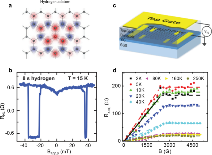
Mccreary et al., Phys.의 허가를 받아 복제했습니다. 레트 목사 109, 186,604(2012). 저작권 2012 미국 화학 학회[23]. (c) 및 (d) Wang et al., Phys. 레트 목사 114, 016,603(2015). Copyright 2015 미국화학회[25]
그래핀의 유도 자기 모멘트. 아 수소로 인한 그래핀의 자기 모멘트의 이론적 예측. ㄴ 15K에서 스핀 수송 측정에 의해 감지된 수소 도핑으로 인한 자기 모멘트. 장치는 8초 수소 도핑 후에 측정되었습니다. ㄷ 원자적으로 평평한 이트륨 철 가넷(YIG) 강자성 박막에 결합된 그래핀 교환의 개략도. d 다양한 온도에서 자기 그래핀에 대한 비정상적인 홀 저항 측정. 아 , b
2D 재료는 수분 및 산소와 같은 환경 조건에 취약합니다. TI 표면 영역의 전도성 표면 상태는 보다 안정적인 2D 재료로 간주됩니다[30]. 또한 TI의 표면 상태는 전하 전류 방향을 통해 스핀 신호를 조작하는 방법을 제공하는 스핀 모멘텀 잠금 특성을 나타냅니다. 더 흥미롭게도, 자기 원자의 도핑 또는 자기 근접 효과에 의한 시간 역전 대칭을 깨면 양자 비정상 홀 효과(QAHE)와 같은 일부 이국적인 현상이 발생할 수 있습니다[18, 31]. Chang et al. [24] Cr 도핑된 자기 TI, Cr0.15에서 처음으로 관찰된 QAHE (Bi0.1 Sb0.9 )1.85 테3 . 그림 2a에서 볼 수 있듯이 자기 유도 TI 밴드의 페르미 레벨을 조정하여 e 홀 컨덕턴스의 고원을 관찰할 수 있습니다. 2 /어 . 측정된 결과는 게이트 조정 가능한 비정상적인 홀 저항이 h의 양자화된 값에 도달함을 보여줍니다. /이 2 자기장이 0일 때(그림 2b). 그러나 도핑된 자기 원자의 스핀 산란 효과는 TI 표면에서 강력한 장거리 자기 질서를 달성하기 위해 제한됩니다. TI와 자성 재료 사이의 자기적 근접성은 도핑 원자 또는 결함의 도입을 방지할 수 있으며, 계면 교환 결합에 의해 장거리 자기 질서를 얻을 수 있습니다. Bi2의 이종 구조에서 계면 자기를 연구하기 위해 스핀 편극 중성자 반사율(PNR)을 사용했습니다. Se3 /EuS(그림 2c) [32]. PNR 결과는 Bi2 Se3 /EuS 이중층은 계면에서 강자성 질서를 가지며, 이 위상적으로 강화된 계면 강자성은 실온까지 지속될 수 있습니다(그림 2d). TI에서 강자성 표면 상태를 구현하면 계면 자기전 효과[33] 및 전기장 유도 이미지 자기 모노폴[34]과 같은 몇 가지 두드러진 현상이 나타날 것으로 예상됩니다.
<그림>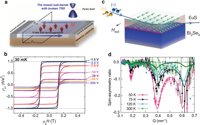
Chang et al., Science 340, 167(2013)의 허가를 받아 재생산 ). Copyright 2013 미국과학진흥협회[24]. c, d Katmis et al., Nature 553, 513(2016)의 허가를 받아 복제했습니다. Copyright 2016 네이처 퍼블리싱 그룹 [32]
TI의 유도 자기 모멘트. 아 자기 TI 박막의 QAHE 개략도. 자화 방향(M)은 빨간색 화살표로 표시됩니다. 필름의 화학 전위는 유전체 기판의 뒷면에 인가되는 게이트 전압에 의해 제어될 수 있습니다. ㄴ Cr0.15의 다른 게이트 전압에서 QAHE의 자기장 의존성 (Bi0.1 Sb0.9 )1.85 테3 영화. ㄷ Bi2에 대한 편광 중성자 반사율(PNR) 실험의 개략도 Se3 /EuS 이중층 필름. d Bi2의 강자성 질서 관찰 Se3 PNR 측정에 의해 측정된 EuS에 대한 자기 근접 결합을 통한 /EuS 이중층 샘플. 아 , b
그래핀 및 TI 외에도 포스포렌[35], 실리신[36, 37], GaSe[38], GaN[39], ZnO[40] 등을 포함한 다른 2D 재료의 고유 결함 및 도펀트에 의해 유도된 자기도 조사되었습니다. 제 1 원리 계산 결과는 공극과 외부 변형 사이의 상호 작용이 포스포린에서 자기를 일으킬 수 있음을 보여주었습니다. 변형이 포스포렌의 지그재그 방향을 따르고 P 공석이 4%에 도달하면 시스템은 자기 모멘트가 ~ 1 μ인 스핀 분극 상태를 나타냅니다. 나 공실당 [35]. 첫 번째 원칙 계산은 또한 정공 도핑이 가전자대 상단에서 전자 상태의 교환 분할로 인해 GaSe 및 GaS에서 강자성 상전이를 유도할 수 있다고 예측했습니다. 자기 모멘트는 1.0 μ만큼 클 수 있습니다. 나 캐리어 당 [38, 39]. 그러나 이러한 조사의 대부분은 이론적 계산에 국한됩니다. 자기 거동을 이해하고 실제 적용을 위한 견고한 2D 실온 강자성 반도체를 탐색하려면 추가 연구, 특히 실험 작업이 필요합니다.
최근에 2D vdW 계열의 또 다른 구성원인 2D 자석이 실험적으로 얻어졌습니다[19, 41]. 이 돌파구는 즉시 2D 자기 분야를 탐구하는 광범위한 관심을 끌었습니다. Xu의 그룹은 처음 보고한 CrI3 단층까지의 단일층은 MOKE(magneto-optical Kerr effect) 기술에 의해 강한 면외 자기 이방성을 갖는 Ising 강자성을 나타냅니다(그림 3a)[42]. 또한 CrI3 단층 및 삼중층 CrI3 이중층은 반강자성이고 이중층은 강자성입니다. Gong et al. 보고된 또 다른 2D 재료, Cr2 Ge2 테6 , 원자층에서 고유한 장거리 강자성 질서를 가지고 있습니다[43]. CrI3와 다름 , Cr2 Ge2 테6 자기 이방성이 작은 2차원 Heisenberg 강자성체로 보고되었다. 그림 3b와 같이 Cr2의 강자성 전이 온도는 Ge2 테6 레이어 수와 관련이 있습니다. 또 다른 인기 있는 2D 강자성체는 Fe3입니다. 게테2 는 두 개의 Te 원자 층 사이에 끼워진 Fe/FeGe/Fe의 층으로 구성된 vdW 강자성 금속입니다[44]. Fe3의 자성을 연구하기 위해 변칙적인 홀 효과가 사용되었습니다. 게테2 , 그리고 결과는 Fe3를 보여줍니다. 게테2 C축에 평행한 쉬운 자화 방향과 230K의 퀴리 온도로 강한 자기 이방성을 갖는다(그림 3c)[45]. 그러나 이들 물질의 퀴리 온도는 상온보다 낮아 소자 적용에 큰 걸림돌이다. 상온 이상의 퀴리 온도를 갖는 것은 2차원 자성 재료의 실제 적용을 위한 전제 조건입니다. 연구원들은 실온 강자성 단층 1 T-VSe2를 준비했습니다. 분자빔 에피택시(MBE)에 의해 [41]. 최근 보고된 소수층 1 T-CrTe2 316K의 높은 퀴리 온도[46]를 나타내어 향후 2D 스핀트로닉 장치의 응용 가능성을 제공합니다. 2D 강자성 물질 외에도 FePS3와 같은 2D 반강자성 물질이 널리 보고되고 있습니다. [47], MnPS3 [48] 및 CrCl3 [49]. 더욱 놀랍게도 Zhang Yuanbo 팀은 최근 고유 자기 위상 절연체 MnBi2에서 자기장 유도 QAHE를 보고했습니다. 테4 [50]. MnBi2 테4 층간 강자성 및 층간 반강자성을 갖는 반강자성체입니다. 양자 전송을 조사하여 깨끗한 5층 MnBi2에서 비정상적인 홀 효과의 정확한 양자화 테4 플레이크는 μ 이상의 적당한 자기장에서 관찰되었습니다. 0 안 저온에서 ~ 6T(그림 3d).
<그림>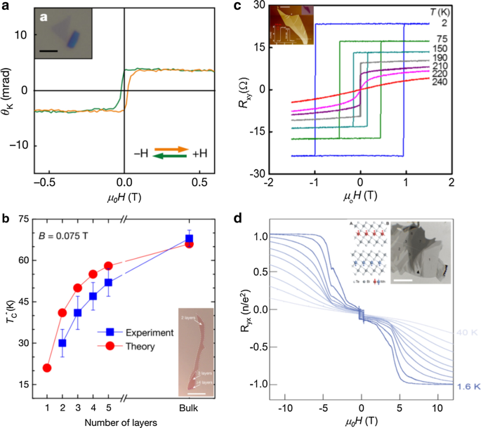
Huang et al.의 허가를 받아 복제, Nature 546, 271(2017) ). Copyright 2017 네이처 퍼블리싱 그룹[42]. ㄴ Gong et al., Nature 546, 265(2017)의 허가를 받아 재생산. Copyright 2017 네이처 퍼블리싱 그룹[43]. ㄷ Fei et al., Nat.의 허가를 받아 복제했습니다. 메이터. 17, 778(2018). Copyright 2018 네이처 퍼블리싱 그룹[44]. d Deng et al., Science 367, 895(2020)의 허가를 받아 복제했습니다. Copyright 2020 미국과학진흥협회[50]
고유한 2D 자석. 아 CrI3에 대한 극자기-광학 커 효과(MOKE) 신호 단층. 삽입된 그림은 분리된 단층 CrI의 광학 이미지를 보여줍니다.3 . ㄴ 전이 온도 TC* Cr2 Ge2 테6 두께가 다른 경우 Kerr 측정에서 얻은 파란색 사각형이 있는 플롯과 이론적 계산에서 얻은 빨간색 원으로 된 플롯이 있습니다. 삽입된 사진은 박리된 Cr2의 광학 이미지를 보여줍니다. Ge2 테6 SiO2의 원자층 /시. ㄷ 12nm 두께의 Fe3에서 측정된 홀 저항의 온도 종속 자기장 스윕 게테2 장치. 삽입된 그림은 SiO2에 있는 대표적인 얇은 FGT 플레이크의 원자력 현미경 이미지를 보여줍니다. . d 5층 MnBi2에서 자기장 유도 QAHE 테4 견본. 자기장 의존 R yx 다양한 온도에서. 삽입은 MnBi2의 결정 구조를 보여줍니다. 테4 및 MnBi2의 소수층 플레이크의 광학 이미지 테4 Al2로 쪼개짐 O3 - 보조 각질 제거 방법. 아
최근 부상하는 2D 재료의 발전과 일부 고급 특성화 기술로 2D 스핀트로닉스 분야가 빠르게 발전할 수 있었습니다[51,52,53]. 스핀트로닉 소자의 구현을 위한 주요 문제는 스핀 전하 변환, 스핀 수송 및 스핀 조작을 포함합니다. 스핀 전류의 효율적인 생성 및 감지는 전기 장치를 대체하는 2D 스핀트로닉 장치 개발의 주요 과제입니다. 스핀 수송은 긴 스핀 수명과 장거리 스핀 전파를 가진 적절한 수송 채널을 원합니다. 스핀 전류를 제어하고 장치 기능을 달성하려면 스핀 조작이 필요합니다.
전기 스핀 주입/검출 또는 SOC에서 비롯된 스핀 홀 효과 및 에델슈타인 효과 활용과 같은 스핀-전하 변환을 달성하기 위해 많은 방법이 제안되었습니다[54,55,56]. 그러나 스핀 홀 효과는 일반적으로 벌크 재료에서 발생하는 반면 에델슈타인 효과는 일반적으로 계면 효과로 간주됩니다[55].
"nonlocal" 및 "local" 측정은 일반적으로 채널 재료에 전기 스핀 주입/검출을 수행하는 데 사용됩니다[14]. 비국소 측정의 경우(그림 4a), 전극 E2는 스핀 인젝터로서의 강자성 금속이고, E3은 스핀 검출기로서의 강자성 전극입니다. 인가된 전류는 전극 E1에서 E2까지 흐르고 E3과 E4는 확산된 순수 스핀 전류 신호를 감지하는 데 사용됩니다. E3와 E4 사이에서 측정된 전압의 극성은 전극 E2와 E3의 자화 구성에 따라 달라집니다. 이 방법은 충전 전류 없이 순수한 스핀 전류를 얻을 수 있는 반면 "로컬" 측정은 스핀 전류와 충전 전류의 혼합 신호를 얻습니다(그림 4b). 전극 E2와 E3의 평행 자화 정렬과 역평행 자화 정렬 사이의 전압 차이는 스핀 전달 신호로 간주됩니다.
<그림>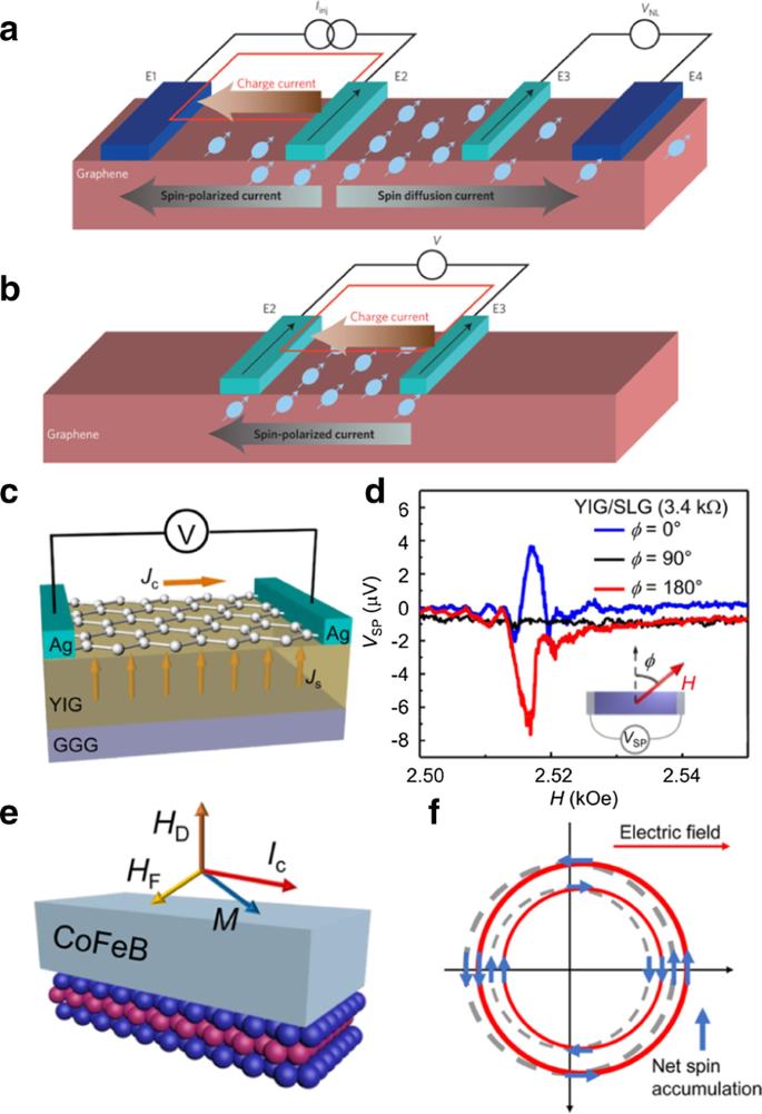
Han et al., Nat. 나노기술. 9, 794(2014). Copyright 2018 네이처 퍼블리싱 그룹[14]. ㄷ , d Mendes et al., Phys.의 허가를 받아 복제했습니다. 레트 목사 115, 226601(2015). 저작권 2015 미국 화학 학회[68]. 이 , f Shao et al., Nano Lett의 허가를 받아 복제했습니다. 16, 7514(2016). Copyright 2016 미국화학회[71]
2D 재료의 스핀 및 전하 변환. 아 비국소 측정 형상을 사용한 전기 스핀 주입 및 감지. ㄴ 로컬 측정 형상을 사용한 전기 스핀 주입 및 감지. ㄷ 강자성 절연체인 YIG에서 그래핀의 스핀-전하 변환. 스핀 전류는 YIG에서 스핀 펌핑에서 생성되고 그래핀에서 전하 전류로 변환됩니다. d YIG/Graphene e에서 측정된 스핀 펌핑 전압의 자기장 의존성 MX2에 대한 SOT 측정 /CoFeB 이중층. MX2 MoS2를 나타냅니다. 및 WSe2 . 에 MX2 경계면에서 Rashba-Edelstein 효과(REE)에 의한 유도된 스핀 축적의 그림 /CoFeB 외부 전기장에서. 아 , b
Hillet al. 연자성 NiFe 전극을 사용하여 그래핀에 스핀을 주입하는 것을 처음 보고했습니다[57]. 그러나 스핀 주입 효율은 약 10% 정도로 상대적으로 낮은 것으로 추정되며, 이는 강자성 금속과 그래핀 간의 전도도 불일치에 기인할 수 있습니다. 그런 다음 일부 연구자들은 Al2와 같은 절연 장벽을 사용할 것을 제안했습니다. O3 또는 계면 스핀 의존 저항을 조정하고 스핀 주입 효율을 향상시키기 위한 층으로서 MgO[58,59,60], 그러나 고품질 산화물 층을 성장시키는 것은 주요 도전과제입니다. 일부 방법은 산화물 층 성장 기술을 개선하거나 TiO2 층과 같은 다른 계면 산화물 층으로 변경하는 데 사용되었습니다. 또는 HfO2 [61, 62]. 그러나 계면 스핀 의존 저항은 여전히 근본적인 문제로 스핀 주입 효율이 낮다. 육각형 질화붕소(h-BN)라는 2차원 절연 물질 중 하나는 그래핀과 유사한 결정 구조를 갖고 있다. 이론 및 실험 연구에 따르면 h-BN을 터널 장벽으로 사용하면 고품질 인터페이스를 생성하고 그래핀의 스핀 주입 효율을 크게 향상시킬 수 있습니다. 소수층 h-BN은 단층 h-BN보다 더 나은 스핀 주입 성능을 나타냅니다[63, 64]. 그럼에도 불구하고 이러한 연구 결과는 실제 적용이 가능하기까지 여전히 큰 공백을 남겨 둡니다. 궁극적으로 완벽한(100%) 스핀 주입을 달성하려면 많은 연구가 필요하며 2D 강자성 재료로 구성된 2D 이종 구조, 2D 터널 장벽 및 2D 전송 채널과 같은 2D 재료는 유망한 방향을 제시합니다.
(역) Rashba-Edelstein 효과는 강력한 SOC에서 비롯되는 계면 효과로, 스핀 전하 변환을 달성하는 데 사용할 수 있습니다[65]. 진성 그래핀은 SOC가 다소 약하지만 근접 효과를 통해 인접 물질의 강한 SOC를 이용하여 효율적인 스핀-전하 변환을 달성할 수 있다[66, 67]. 도 4c에 도시된 바와 같이 그래핀이 강자성 절연체 YIG에 인접해 있을 때 스핀 펌핑을 통해 YIG 층에 스핀 전류가 생성되고 역 에델슈타인 효과에 의해 그래핀 내 전하 전류로 변환된다[68]. 그림 4d는 YIG/그래핀 장치에서 필드의 함수로 스핀 펌핑 전압 곡선을 보여줍니다. 스핀 펌핑 전압은 그래핀 채널에 수직인 자기장에서 감지할 수 있습니다. 또한 그래핀 채널을 따라 외부 자기장이 회전하면 스핀 펌핑 전압이 없습니다. 또한 그래핀 표면에 적용된 이온성 액체 게이팅은 그래핀의 특성을 분명히 조절하여 YIG/그래핀의 스핀-전하 변환 효율을 변경할 수 있습니다[56].
그래핀과 달리 SOC가 강한 TMDC는 스핀-전하 변환을 달성하기 위한 유망한 재료로 간주됩니다[69, 70]. 단층 TMDC(MoS2)에서 큰 스핀-궤도 토크(SOT) 또는 WSe2 )/CoFeB 이중층 구조는 Rashba-Edelstein 효과로 인한 전류 유도 스핀 축적을 통해 생성되었습니다(그림 4e, f) [71]. 자기장과 유사한 토크와 감쇠와 같은 토크는 2차 고조파 측정을 통해 결정되었으며, 결과는 대면적 단층 TMDC가 자화 반전 효율이 높기 때문에 잠재적으로 응용할 수 있음을 보여줍니다. 또한, 스핀-토크 강자성 공명(ST-FMR) 기술은 TMDC의 스핀 및 전하 변환을 조사하는 데 사용되었습니다. 예를 들어, 흥미로운 ST-FMR 결과는 SOT가 Wte2의 결정 대칭을 통해 제어될 수 있음을 보여줍니다. Wte2에서 / 퍼멀로이 이중층. Wte2의 낮은 대칭 축을 따라 전류가 인가될 때 , 면외 반감쇠 토크가 생성될 수 있습니다[72]. TI 표면 상태에서 스핀 모멘텀 잠금 속성은 SOT를 통해 인접한 재료로 스핀 전류 주입을 달성하는 데 유용합니다. 스핀 분극 방향과 충전 전류 방향 사이의 강한 상관 관계로 인해 스핀 방향은 TI의 충전 전류에 의해 조작될 수 있습니다. 2차 고조파 측정, 스핀 펌핑 및 ST-FMR을 포함하여 스핀 전하 변환을 조사하기 위해 다양한 측정 기술이 사용되었습니다. 이러한 측정 결과는 TMDC 및 TI와 같은 2D 재료에서 효율적인 SOT를 생성할 수 있음을 보여줍니다.
스핀 수송의 핵심은 스핀 확산 길이와 스핀 완화 시간이 긴 유리한 스핀 수송 채널을 얻는 것입니다. 스핀 이완은 운동량 산란에 의해 발생하므로 SOC가 약한 그래핀은 스핀 수송에 이상적인 재료로 간주된다[14, 73]. Tombros et al. [74] 2007년 상온에서 측방 단일 그래핀 스핀 밸브에서 전자적 스핀 수송 및 스핀 세차를 비국소 측정에 의해 실현하였다. 얇은 Al2 O3 산화물 층을 장벽으로, 그래핀 시트를 스핀 수송 채널로 사용합니다. 그림 5c의 측정 신호는 스핀 주입 및 스핀 검출용 강자성 전극이 평행한 자화를 가질 경우 접점 1과 2에서 측정한 비국부 저항이 양의 값을 가짐을 보여줍니다. 스핀 주입 및 스핀 검출용 강자성 전극이 역평행 자화를 갖는 경우 비국부 저항은 음의 값을 나타냅니다. Hanle 스핀 세차 운동은 스핀 확산 길이와 스핀 수명을 결정하는 데 사용할 수 있습니다. 그림 5d와 같이 스핀 수명(τ sf ) 및 스핀 이완 길이(λ sf )은 실온에서 측면 단일 그래핀 스핀 밸브에서 각각 125ps 및 1.3μm입니다. 또한, 게이트는 스핀 이완 길이와 스핀 수명을 향상시키는 데 사용할 수 있습니다[75, 76]. 이론은 순수한 그래핀의 스핀 수명이 1μs에 도달할 수 있는 반면 보고된 실험 값은 피코초에서 수 나노초 범위라고 예측했습니다.
<그림>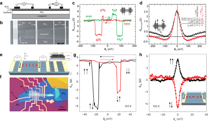
Tombros et al., Nature 448, 571(2007)의 허가를 받아 복제 ). Copyright 2007 네이처 퍼블리싱 그룹[74]. 이 –h Avser et al., Nat.의 허가를 받아 복제했습니다. 물리. 13, 888(2017). Copyright 2017 네이처 퍼블리싱 그룹 [84]
측면 스핀 밸브에서의 스핀 수송. 아 비국소 스핀 수송 측정 기하학. 전극 3에서 Al2를 통해 전류가 주입됩니다. O3 그래핀으로 장벽을 만들고 접촉 4에서 추출됩니다. b 단층 그래핀을 스핀 수송 채널로, Co를 4개의 강자성 전극으로 사용하는 4단자 스핀 밸브의 주사 전자 현미경 사진. ㄷ 4.2K에서 비국소 스핀 밸브 신호. 전극의 자기 구성은 두 스윕 방향에 대해 설명됩니다. d 수직 자기장 B의 함수로 측정된 비국소 기하학의 Hanle 스핀 세차 운동 z 병렬 구성의 경우. 이 흑색 인 스핀 밸브의 개략도. 삽입된 그림은 이종 구조의 개략도를 보여줍니다. 에 장치의 광학 이미지입니다. 지 면내 자기장의 함수로서의 비국소 스핀 밸브 신호. 주입기와 검출기 전극의 상대적인 자화는 수직 화살표로 표시되고 수평 화살표는 자기장의 스위핑 방향을 나타냅니다. 아 수직 자기장 B의 함수로 측정된 비국소 기하학의 Hanle 스핀 세차 운동 z 병렬 및 역병렬 구성용. 삽입 된 그림은 적용된 자기장 아래에서 회전 세차를 보여줍니다. 아 –d
많은 개선된 방법이 스핀 확산 길이와 스핀 수명을 늘리는 데 사용되며 일부 장치는 이미 마이크로미터 범위에서 긴 스핀 확산 길이를 나타냅니다[13, 77, 78]. 예를 들어, SiC에서 에피택셜 성장한 그래핀은 이동도가 높아 최대 75%의 스핀 수송 효율과 100μm를 초과하는 스핀 확산 길이를 나타냅니다[79]. h-BN/graphene/h-BN 이종구조는 상온에서 스핀 확산 길이가 30.5μm에 도달할 수 있는 장거리 스핀 수송 성능을 나타냅니다[13]. 2D 재료의 스핀 전송은 전기장을 적용하여 변조될 수 있는 확산/드리프트의 영향을 받을 수 있습니다. Ingla-Aynés et al. [80]은 캐리어 드리프트를 사용하여 h-BN 캡슐화된 이중층 그래핀에서 최대 90μm의 스핀 이완 길이를 보고했습니다. 그러나 고유 그래핀의 약한 SOC와 제로 밴드갭은 반도체 스핀 장치에 대한 전망을 제한합니다. 흑린은 상당한 직접 밴드갭과 1000cm의 실온 이동성을 가지고 있습니다. 2 V −1 s −1 , 이는 이상적인 반도체 스핀트로닉 재료를 만듭니다[81,82,83]. Avsar et al. [84]는 초박형 흑색 인 시트를 기반으로 측면 스핀 밸브를 구성하고 비국소 기하학을 통해 실온에서 스핀 수송 특성을 측정했습니다(그림 5e, f). 그림 5g의 전자 스핀 수송은 강자성체의 자화 방향이 전환됨에 따라 비국부 저항이 ΔR의 변화를 가짐을 보여줍니다. ≈ 15Ω. 이 외에도 Hanle 스핀 세차 운동은 최대 4ns의 스핀 이완 시간과 6μm를 초과하는 스핀 이완 길이를 보여줍니다(그림 5h). 흑린의 스핀 수송은 전하 캐리어 농도와 밀접한 관련이 있으므로 전기장을 인가하여 스핀 신호를 제어할 수 있습니다.
스핀 조작을 실현하는 것이 효과적인 장치 기능화의 핵심입니다. 게이트 전압을 적용하면 물질의 캐리어 농도를 제어할 수 있으며, 이는 스핀 신호를 조작하는 데 사용할 수 있습니다[85, 86]. 게이트 전압을 인가함으로써 스핀 수송 매개변수의 조정을 실현하기 위해 스핀 수송 채널로서 다양한 2D 재료가 조사되었습니다. 예를 들어 바이어스 유도 그래핀은 강자성체/이중층 h-BN/그래핀/h-BN 이종구조에서 최대 100%까지 스핀 주입 및 검출 분극을 얻을 수 있습니다[64]. A gate-tunable spin valve based on black phosphorus can reach a spin relaxation time in the nanosecond range and a long spin relaxation length [84]. For a semiconducting MoS2 channel, applying a gate voltage can still get a relatively long spin-diffusion length, larger than 200 nm [70]. However, a suitable spin field-effect device requires a clear switching ratio, which is a challenge for graphene and even for semiconducting 2D materials [87, 88].
To solve this issue, a vdW heterostructure based on atomically thin graphene and semiconducting MoS2 has been developed to achieve a spin field-effect switch via applying a gate voltage (Fig. 6a) [89]. In this structure, the superior spin transport properties of graphene and the strong SOC of MoS2 are combined. The applied gate voltage can change the conductivity of MoS2 and spin absorption during the spin transport, which results in switching of the spin current between ON and OFF states in the graphene channel (Fig. 6b). Another research effort produced a similar report about the graphene/MoS2 vdW heterostructure. In this report, an electric gate control of the spin current and spin lifetime in the graphene/MoS2 heterostructure was achieved at room temperature [90]. Moreover, that report pointed out that the mechanism of gate tunable spin parameters stemmed from gate tuning of the Schottky barrier at the MoS2 /graphene interface and MoS2 channel conductivity.

source contact. ㄴ Effective B SO V의 함수로 g . The inset shows the surface carrier distribution in the Cr-TI layer under V g = − 10 V, + 3 V, and + 10 V. a –ㄷ Reproduced with permission from Yan et al., Nat. Commun. 7, 1 (2016). Copyright 2016 Nature Publishing Group [89]. d , e Reproduced with permission from Fan et al., Nat. Mater. 13, 699 (2014). Copyright 2014 Nature Publishing Group [95]. 에 , 지 Reproduced with permission from Fan et al., Nat. Nanotechnol. 11, 352 (2016). Copyright 2016 Nature Publishing Group [96]
Spin manipulation. 아 Schematic illustration of a 2D spin field-effect switch based on a vdW heterostructure of graphene/MoS2 with a typical nonlocal magnetoresistance measurement. ㄴ The nonlocal resistance R nl switches between R P 및 R AP for parallel and antiparallel magnetization orientations of the Co electrodes. The spin signal is calculated as ΔR nl =R P − R AP . ㄷ The plot with blue circles shows the gate modulation of the spin signal ΔR nl . The solid black line represents the sheet conductivity of the MoS2 V의 함수로 g . The insets show the spin current path in the OFF and ON states of MoS2 . d Schematic illustration of SOT-induced magnetization switching in a Cr-doped TI bilayer heterostructure. The inset shows illustrations of the Hall bar device and the measurement setting. 이 Experimental results of SOT-induced magnetization switching by an in-plane direct current at 1.9 K while applying a constant in-plane external magnetic field B y during the measurement. The inset shows an enlarged version of the circled part in the figure. 에 3D schematic of the Hall bar structure of the Al2 O3 /Cr-TI/GaAs stack with a top Au gate electrode. A gate voltage of V g can be applied between the top gate and the
Current-induced SOT is regarded as another efficient strategy to manipulate spin. The spin current, generated by the spin Hall effect within the heavy metals or the Rashba effect at the interfaces, can exert a spin torque to ferromagnets and thereby realize magnetization switching [91,92,93]. Efficient current-induced magnetization switching via SOT may lead to innovative spintronic applications. Due to strong SOC and time-inversion symmetry breaking, magnetically doped TIs are being considered as a promising material to manipulate spin signals via SOT [94]. Wang’s group first experimentally demonstrated a magnetization switching induced by an in-plane current in an epitaxial Cr-doped TI (Bi0.5 Sb0. 5)2 테3 /(Cr0.08 Bi0.54 Sb0.38 )2 테3 bilayer film (Fig. 6c) [95]. The spin Hall angle in the Cr-doped TI film, ranging from 140 to 425, is almost three orders of magnitude larger than that in heavy metal/ferromagnetic heterostructures, and the critical switching current density is below 8.9 × 10⁴ A cm −2 at 1.9 K (Fig. 6d). Furthermore, this team also reported an effective electric field control of SOT in a Cr-doped (Bi0.5 Sb0.42 )2 테3 thin film epitaxially grown on GaAs substrate (Fig. 6e) [96]. The gate effect on the magnetization switching was investigated by scanning gate voltage under a constant current and an applied in-plane magnetic field in the film (Fig. 6f). The SOT intensity depends strongly on the spin-polarized surface current in the thin film, and it can be modulated within a suitable gate voltage range. The effective electric field control of SOT in the TI-based magnetic structures has potential applications in magnetic memory and logic devices.
In addition, electrical control of emerged 2D magnets has also been investigated. For example, utilizing electric fields or electrostatic doping can achieve the magnetic conversion of bilayer CrI3 antiferromagnetic to ferromagnetic [97]. The coercivity and saturation field of few-layer Cr2 Ge2 Te6 can be modulated via ionic liquid gating [98]. In contrast to magnetic semiconductor, electrostatic doping can be used to control the carrier concentrations of the ferromagnetic metal, and the ferromagnetic transition temperature of Fe3 GeTe2 can be dramatically raised to room temperature via an ionic gate [99]. The emergence and research of 2D magnets provide a new platform for engineering next-generation 2D spintronic devices.
2D materials exhibit great potential for the engineering of next-generation 2D spintronic devices. Graphene with high electron/hole mobility, long spin lifetimes, and long diffusion lengths is a promising candidate for a spin channel. Moreover, graphene can gain magnetism by introducing adatoms, or magnetic proximity effect [23, 25]. The carrier density in proximity-induced ferromagnetic graphene can be modulated by gating, allowing to observe Fermi energy dependence of the anomalous Hall effect conductivity. This result can help understand the physical origin of anomalous Hall effect in 2D Dirac fermion systems. Realizing a ferromagnetic surface state in a TI is predicted to allow several prominent phenomena to emerge, such as the interfacial magnetoelectric effect [33], and the electric field-induced image magnetic monopole [34]. However, the current technology of inducing magnetism in TI is confined to low temperatures, which restrict its potential for applications. A key requirement for useful applications is the generation of room temperature ferromagnetism in the TI. The PNR result shows that the Bi2 Se3 /EuS bilayer has a ferromagnetic order at the interface, and this topologically enhanced interfacial ferromagnetism can persist up to room temperature [32]. The topological magnetoelectric response in such an engineered TI could allow efficient manipulation of the magnetization dynamics by an electric field, providing an energy-efficient topological control mechanism for future spin-based technologies.
The STT, and tunnel magnetoresistance (TMR) effects offer alternative approaches for write and read-out operations. The STT effect refers to the reorientation of the magnetization of ferromagnetic materials via the transfer of spin angular momenta. Efficient current-induced magnetization switching via SOT may lead to innovative spintronic applications [71, 100]. Due to strong SOC and time-inversion symmetry breaking, magnetically doped TIs are being considered as a promising material to manipulate spin signals via SOT [93]. TMR refers to magnetization-dependent magnetoresistance behavior. A high TMR ratio is the key to achieve spintronic devices with higher sensitivity, lower energy consumption. 2D materials with high-quality crystal and sharp interfaces can achieve some new functionalities such as spin filtering. The 2D vdW MTJ consists of a 2D magnetic CrI3 layer as a spin filtering tunnel barrier, which reaches a value of TMR up 19,000% [101]. Progress in the fabrication of graphene-based and other 2D heterostructures has led to the optimization of long-distance spin diffusion (up to tens of micrometres), as well as directional guiding of the spin current [13, 64]. Spin manipulation, electrical gating [56], electrical field induced drift [80], SOT-induced switching [95, 96], and the magnetic proximity effect [25, 32] have been explored to develop next-generation MRAM.
Great efforts have been made to search for new 2D spintronic devices. According to the function, 2D spintronic devices can be classified as memory storage or logic devices. Here we focus on several important 2D spintronic devices, including the 2D magnetic tunnel junction (MTJ), 2D spin field-effect transistor (sFET), and 2D spin logic gate.
The discovery of the GMR opens the door for 2D spintronics. However, TMR has a stronger magnetoresistance ratio than GMR, so TMR holds greater potential in magnetic storage applications. The TMR structure consists of two ferromagnetic layers and an intermediate insulating layer, which is called the MTJ. The tunneling probability is related to the density of states near the Fermi energy in the ferromagnetic layers. When the two magnetic layers are parallel, the similar density of states for each spin-state can provide more available states for tunneling, resulting in a low resistance state. On the other hand, when the layers are antiparallel, a mismatch between spin channels of the source and sink will result in a high resistance state. Some issues in traditional thin-film MTJs limit the achievement of a high TMR ratio, such as the quality of the insulation barrier and the thermal stability [102]. 2D materials with high-quality crystal and sharp interfaces may offer promising routes to address these issues and even achieve some new functionalities such as spin filtering.
Karpan et al. first explored graphene layers as the barrier in vertical MTJ by computational means in 2007 [103]. They proposed a match between the band structure of graphene and that of nickel, predicting a large spin polarization close to 100%, which can result in a large TMR up to 500%. However, the subsequent experimental results show that the MTJs based on graphene exhibit a very low TMR. Compared to monolayer or bilayer graphene, the few-layer MTJ holds the highest recorded TMR signal of up to 31% in graphene-based MTJs [11, 15]. In addition to graphene, some other 2D materials have been explored as tunneling barrier layers, including insulating h-BN and semiconducting TMDCs [104, 105]. Piquemal-Banci et al. [63] fabricated Fe/h-BN/Co junctions where the h-BN monolayer was directly grown on Fe by using the chemical vapor deposition (CVD) method, observing large spin signals of TMR and the spin polarization of P ~ 17%. MTJs based on MoS2 or WSe2 were reported to have only a few percent of the TMR signal; further exploration is needed to achieve a high TMR ratio.
Emerging 2D magnetic materials exhibit many surprising properties. When the magnetizations in bilayer CrI3 are switched to different magnetic configurations (Fig. 7a), the MTJ based on CrI3 exhibits a giant TMR produced by the spin-filtering effect [101, 106, 107]. As demonstrated in Fig. 7b, the 2D vdW MTJ consists of a 2D magnetic CrI3 layer as a spin filtering tunnel barrier, graphene as a contact electrode, and h-BN as an encapsulation layer to prevent device degradation. The transport result shows that the TMR is enhanced as the CrI3 layer thickness increases, and it reaches a value of 19,000% in four-layer CrI3 based MTJ at low temperature (Fig. 7c) [101]. Subsequently, Xu’s group also reported gate-tunable TMR in a dual-gated MTJ structure based on four-layer CrI3 . The TMR can be modulated from 17,000 to 57,000% by varying the gate voltages in a fixed magnetic field [108, 109]. Moreover, with few-layer Fe3 GeTe2 serving as ferromagnetic electrodes, the TMR in Fe3 GeTe2 /h-BN/Fe3 GeTe2 heterostructures can reach 160% at low temperature [110]. More interestingly, Zhou et al. reported a theoretical investigation of a VSe2 /MoS2 /VSe2 heterojunction, where the VSe2 monolayer acts as a room-temperature ferromagnet, and the large TMR can reach 846% at 300 K [111]. On the other hand, the strong spin Hall conductivity of MoS2 holds potential to switch the magnetization of the VSe2 free layer by SOT. Therefore, they put forward the concept of SOT vdW MTJ with faster reading and writing operations, which offers new opportunities for 2D spintronic devices.

Reproduced with permission from Song et al., Science (2018). Copyright 2018 The American Association for the Advancement of Science [101]. ㄷ , d Reproduced with permission from Wen et al., Phys. Rev. Appl. 5, 044003 (2016). Copyright 2016 American Chemical Society [118]
2D spintronic Devices. 아 Magnetic states of bilayer CrI3 with different external magnetic fields. ㄴ Schematic illustration of a 2D spin-filter MTJ with bilayer CrI3 sandwiched between graphene contact. ㄷ Tunneling current of a bilayer CrI3 sf-MTJ at selected magnetic fields. The top inset shows an optical image of the device, and the bottom inset shows the schematic of the magnetic configuration in different magnetic fields. d Diagram of a proposed 2D XOR spin logic gate, where A, B, and M are ferromagnetic electrodes on top of a spin transport channel. 나 s 그리고 나 밖 denote the injection and detection currents, respectively. The magnetizations of the electrodes are input logic 1 and 0. The detected current I 밖 serves as the logic output. 이 나 밖 measured as a function of H . Vertical arrows indicate the magnetization states of A and B. The top-left inset shows the table of XOR logic operation. 아 , b
Datta and Das first proposed the idea of the sFET in 1990 [112]. The sFET consists of the source and sink ferromagnetic electrodes, and a two-dimensional electron gas (2DEG) channel which can be controlled by an electrical gate. The gate voltage can result in a spin precession and, consequently, a change in the spin polarization of the current on the channel. Since switching the current through the device requires only little energy and a short time, sFET is expected to be a 2D spintronic device with low power consumption and high computing speed.
As mentioned in the previous section, graphene with high carrier concentration and weak SOC is considered to be a promising candidate as a spin transport channel [113]. Michetti et al. [76] designed a double-gate field-effect transistor structure, where bilayer graphene acts as the transport channel. Theoretical analysis shows that the spin precession of carriers in the graphene channel can be turned on and off by the application of a differential gate voltage. Experimentally, Avsar et al. first reported a dual-gated bilayer graphene structure with h-BN as a dielectric layer, where the spin current propagation in bilayer graphene channel can be controlled by exerting a vertical electric field [114]. The transport results show that the spin-relaxation time decreases monotonically as the carrier concentration increases, and the spin signal exhibits a rapid decrease, eventually becoming undetectable close to the charge neutrality point. A suitable spin field-effect device requires a clear switching ratio, which is a challenge for graphene.
To solve this issue, a graphene/MoS2 heterostructure has been developed to achieve a spin field-effect switch via applying a gate voltage. Two independent groups demonstrated that the applied gate voltage can change the conductivity of MoS2 and result in spin absorption during the spin transport, which gives rise to switching the spin current between ON and OFF states in the graphene channel [89]. Due to the low spin injection efficiency and rapid spin relaxation in channels, it is a challenge to achieve a large high-to-low conductance ratio in 2D sFET device. However, the discovery of 2D magnetic crystals provides new opportunities to explore new 2D spintronic devices. Kin Fai Mak’s group reported a spin tunnel field-effect transistor (sTFET) based on a dual-gated graphene/CrI3 /graphene heterostructure [115]. By using bilayer CrI3 as a magnetic tunnel barrier, the applied gate voltage can switch magnetization configurations of bilayer CrI3 from interlayer antiferromagnetic to ferromagnetic states under a constant magnetic field near the spin-flip transition. Distinct from conventional spin transistors, these devices rely on electrically controlling the magnetization configuration switching rather than the signal of spin current in the channel. This technique allows the sTFET devices to achieve a large high–low conductance ratio approaching 400%, which provides a new approach for exploring memory applications.
Dery and Sham first reported a spin logic device based on an “exclusive or” (XOR) gate [116]. The XOR logic gate structure includes a semiconductor channel and three ferromagnetic terminals. An XOR logic operation can be implemented by different spin accumulations, which is caused by different magnetization configurations of the input terminals [117]. Experimentally, the proposed three-terminal XOR logic gate achieved logical operations in a graphene spintronic device at room temperature [117,118,119]. As shown in Fig. 7c, the device includes single-layer graphene as the channel, and three ferromagnetic terminals composed of A, B, and M Co electrodes with MgO tunnel barriers. The magnetization of the electrodes A and B represents the input states 0 or 1, and the current of the electrode M acts as the output state. The magnetizations of input electrodes A and B will be switched by varying an applied external magnetic field, which results in a different spin accumulation in the M electrode, corresponding to a different output current. If the input A and B electrodes have identical contributions to the output M electrode, then the current in the output ferromagnetic terminal has a detectable value only when the magnetization of input ferromagnetic terminals are antiparallel (01 or 10). When the magnetizations of the input ferromagnetic terminals are parallel (00 or 11), the output current is almost zero. Therefore, the XOR logic operation can be achieved (Fig. 7d).
Dery et al. further designed a reconfigurable magnetologic gate with five-terminal structure combining two XOR gates-XOR (A, X) and XOR (B, Y) with a shared output terminal, M [119]. Similar to the three-terminal XOR logic gate, the different magnetic configurations of input electrodes give rise to the different spin accumulation in the output terminal M, which results in different output signals. By analogy, a finite number of these XOR gates can be used to implement any binary logic function. Subsequently, other groups extended this theoretical design to experimental studies by constructing graphene spin logic gates [120,121,122]. Various modeling, simulation, and experimental explorations of 2D spin logic gates have helped to accelerate the progress toward building practical spin logic applications. However, two key issues remain in the research of graphene spin logic gates. The first one is to balance the contributions of two input terminals to the output one. The other one is to eliminate the influence of background signals on the output.
As discussed above, much theoretical and experimental research has been carried out to explore spintronics based on 2D materials, and considerable progress has been achieved [15, 123, 124]. However, great challenges still need to be addressed for the practical application of 2D memory and logic applications. We now discuss three of these:physical mechanisms, materials science, and device engineering.
Due to the complexity of the experiments, the proposed theoretical research and experimental results usually have large discrepancies. For example, based on the mechanism of spin relaxation, theory predicted that the spin lifetime for pristine graphene would be up to 1 μs, whereas experimental values range from tens of picoseconds to a few nanoseconds [14, 57, 103]. Furthermore, the spin injection efficiency of graphene measured experimentally ranges from a few percent to 10%, which is far smaller than the theoretical prediction value of 60–80% [125]. These differences indicate that more in-depth physical mechanisms and accurate theoretical models need to be proposed and developed to better guide the research direction and analyze the experimental results.
2D materials provide an ideal platform to construct various heterostructures for spintronic applications. However, there are still many major problems in 2D materials. For example, stability is a great challenge for 2D materials. Most 2D materials of thickness close to the atomic level are susceptible to moisture, oxygenation, and temperature, especially the recently emerging 2D magnetic materials, which must be peeled off in a glove box with ultra-low water and oxygen content. Besides this, most currently available 2D magnets rely on mechanical exfoliation, and their low magnetic transition temperature is far below room temperature. These are significant limitations because stability in air, convenient wafer-scale synthesis, and operation above room temperature are prerequisites for 2D materials used in practical applications.
Breakthroughs have been made in the fundamental study of 2D spintronics, such as enhanced spin injection efficiency by using 2D tunnel barriers h-BN, long spin diffusion length up to 30 μm at room temperature in graphene-based 2D heterostructures [13], and high TMR up to 19,000% by using 2D magnets as spin filter barriers [101]. Based on the study of 2D spintronic devices, it is promising to develop the low-power device applications, including advanced magnetic memories and spin logic circuits, which are compatible with the existing complementary metal-oxide semiconductor (CMOS) electronics. However, the design and application of functional 2D spintronic devices are still in the early theoretical prediction and proof-of-concept stage.
2D spintronics is an important scientific research field with many potential applications for future technologies. As mentioned above, considerable challenges currently remain, but there are also many opportunities. Spin valves based on graphene as the spin transport channel can exhibit a long spin diffusion length up to 30 mm at room temperature [13]. Magnetic tunnel junctions with four-layer CrI3 as spin filter tunneling barriers show giant TMR up to 19,000% at low temperatures [101]. The magnetic transition temperature of Fe3 GeTe2 can reach above room temperature via an ionic liquid gate or when tailored by a TI [99, 126]. Spin-polarized current can be injected from WTe2 into magnetic substrates by SOT switching [127]. New concepts of spin tunneling field-effect transistors based on 2D magnets CrI3 have been proposed as well. The demonstration of giant TMR, the efficient voltage control of 2D magnetism, and the magnetization switching in 2D magnets by STT or SOT all open up opportunities for potential next-generation spintronic devices based on atomically thin vdW crystals [21, 100].
The study about the magnetic properties of 2D materials is of great significance to the development of 2D spintronics. The magnetic interaction in graphene and TIs has scarcely been explored, and recently discovered 2D magnets also provide an ideal platform to study 2D magnetism. Great progress has been made in 2D spintronics in recent decades, especially in graphene spintronics. However, the origin of spin relaxation in graphene is still a major open question, and further improvement in the spin lifetime and spin diffusion length remains an important research direction for graphene-based spintronic devices. The practical application of 2D spintronic devices still requires meeting great challenges, including related physical mechanisms, materials science, and device engineering. The development of technology, the improvement of theoretical models, and the exploration of new materials all provide more opportunities for new-generation 2D spintronic device applications in the future.
해당 없음.
2차원
Giant magnetoresistance effect
Spin-transfer-torque magnetoresistive random-access memory
Van der Waals
Spin–orbit coupling
전이금속 디칼코게나이드
Topological insulators
초전도 양자 간섭 소자
Yttrium iron garnet
Quantum anomalous Hall effect
Spin-polarized neutron reflectivity
Magneto-optical Kerr effect
분자빔 에피택시
Hexagonal boron nitride
Spin–orbit torque
Spin-torque ferromagnetic resonance
Magnetic tunnel junction
Spin field-effect transistor
Tunneling magnetoresistance
화학 기상 증착
2차원 전자 가스
Spin tunnel field-effect transistor
Exclusive or
상보성 금속 산화물 반도체
나노물질
Advanced Strength of Materials 책(도버 토목 및 기계 공학) 재료의 고급 강도 도서(도버 토목 및 기계 공학)의 PDF를 구입하거나 다운로드하시겠습니까? 책 구매 링크는 아래와 같습니다. 제품 설명 40년 전, 당시 매사추세츠 공과 대학의 기계 공학 교수인 J.P. Den Hartog는 전 세계 공과 대학에서 여전히 큰 인기를 누리고 있는 기초 교재인 Strength of Materials를 저술했습니다. 학급 보조 자료로 널리 사용되는 이 책은 전 세계의 엔지니어들 사이에서 가장 좋아하는 안내서
접합은 특히 제품 또는 하위 구성 요소가 둘 이상의 재료 사이에 단단히 고정되어야 하는 경우 제조에서 중요한 프로세스입니다. 고려해야 할 몇 가지 결합 방법이 있지만 화학적 결합 공정은 일반적으로 훨씬 더 강화된 강화, 설계 유연성 및 전반적으로 향상된 성능을 제공합니다. 이 게시물에서는 열경화성 폴리우레탄으로 접착할 때의 이점에 대해 설명하고 제품 설계 프로세스에 도움이 되는 통찰력을 제공합니다. 열경화성 폴리우레탄을 다른 재료에 접착하는 방법 캐스트 또는 반응 사출 성형(RIM) 제품과 관련하여 열경화성 폴리우레탄은 일반적