우리는 나노다이아몬드에 질소-공석-질소 중심을 형성하는 고압, 고온 소결 기술을 시연합니다. 평균 크기가 25nm인 다결정 다이아몬드 나노입자 전구체는 폭발 충격파에 의해 생성됩니다. 이 나노 입자는 7GPa의 압력과 1300°C의 온도에서 에탄올이 있는 상태에서 소결되어 실질적으로 더 큰(3-4배) 다이아몬드 결정자를 생성합니다. 기록된 스펙트럼 특성은 개선된 결정질 품질을 보여줍니다. 존재하는 결함의 유형도 변화하는 것으로 관찰됩니다. 전구체 물질에 대해 존재하는 질소-공석 및 실리콘-공석 중심의 특징적인 스펙트럼 특징은 사라진다. 두 가지 새로운 특징이 나타납니다. (1) I로 인한 전자 상자성 공명 특성 삼중항 초미세 구조를 갖는 상자성 치환 질소(P1 중심에 스핀 1/2) =1 질소 핵 스핀의 자기 모멘트 및 (2) 질소-공석-질소 중심의 녹색 스펙트럼 광발광 서명. 이 생산 방법은 기존의 고에너지 입자 빔 조사에 대한 강력한 대안입니다. 광학 생체 표지 응용 프로그램에 유리한 특성을 가진 순수한 녹색 형광 나노다이아몬드를 쉽게 생산하는 데 사용할 수 있습니다.
소개
질소 불순물과 공석은 대부분의 천연 및 합성 다이아몬드의 주된 결함입니다. 개별 결함은 집합적으로 최대 6개의 소단위가 있는 결함 복합체를 형성할 수 있습니다[1, 2]. 이러한 결함 복합체 중 질소 결손(NV
−
) 및 그보다 적지만 NVN(nitrogen-vacancy-nitrogen) 중심은 각각 깜박이지 않는 적색 및 녹색 광발광으로 인해 상당한 관심을 끌고 있습니다[3, 4]. NV
−
NVN은 나노다이아몬드에서 제어 가능하게 생성될 수 있습니다. 나노다이아몬드는 무독성 나노입자로 널리 알려져 있으므로 생물의학 분야에서 장기간 추적 가능한 표지로 사용될 수 있습니다[5]. NV가 있는 나노결정
−
컬러 센터는 양자 감지에도 사용됩니다[3].
기존의 전이 금속 용매 촉매를 사용한 고압, 고온(HPHT) 다이아몬드 합성은 표준 산업 기술입니다. 고급 격자 매개변수로 다이아몬드 결정을 성장시키기 위해 많은 실험실에서 이용됩니다. 그러나 최근 들어 다양한 비전통 금속 촉매가 널리 사용되기 시작하였다[6]. 이러한 방법을 사용하면 질소 함유 유기 첨가제와 금속 게터를 사용하여 높은 질소 함량(최대 ~ 1000ppm)에서 훨씬 낮은 수준(~ 50ppm)까지 다이아몬드를 제어 가능하게 도핑할 수 있습니다. [7, 8] . HPHT는 또한 다이아몬드 결정을 어닐링하고 결정 품질을 개선하고 변색하고 나노 결정을 더 큰 다결정으로 소결하는 데 사용됩니다.
온도(및 압력)의 영향으로 개별 질소 결함을 다이아몬드의 더 큰 복합체로 그룹화하는 것이 광범위하게 연구되었습니다. 이러한 복합체는 완료된 결정화 과정의 온도 이력을 기록하는 특정 마커 역할을 할 수 있습니다[1]. NVN 및 NV
−
중심은 순수한 질소 함유 다이아몬드에 고에너지(2–14meV) 전자 또는 양성자 또는 ~ 40keV 중이온을 조사하여 만들 수 있습니다. 조사는 다이아몬드 격자에 공석을 생성합니다. 500–2000°C 범위의 온도에서 샘플을 후속적으로 어닐링하면 결함이 그룹화됩니다[3, 9, 10]. 현재 NV
–
양산 중 또는 NVN 함유 나노다이아몬드는 일반적으로 고에너지 전자 조사에 의해 실현된다. 그러나 이 프로세스는 비용이 많이 들고 시간이 많이 걸리며 특정 샘플 준비가 필요합니다. 따라서 입자 조사가 필요하지 않은 나노다이아몬드의 색상 중심 생성을 위한 대체 방법을 개발할 가치가 있습니다.
C-H-O 액체 첨가제가 있는 상태에서 5nm 폭발 나노다이아몬드(DND)를 소결하여 서브미크론 크기의 다이아몬드 결정을 제조하는 새로운 방법이 최근 도입되었습니다[11, 12]. HPHT 소결 조건에서 첨가된 C-H-O 유기물은 빠른 다이아몬드 재결정을 유도하는 초임계 유체로 작용합니다. 빠른 재결정화는 더 높은 밀도의 공석을 동반합니다[13]. 그러나 이 방법은 전구체 5nm DND에 존재하는 깨끗한 색상 중심을 억제합니다[14]. 따라서 HPHT 소결 과정에서 이러한 결함을 보존하거나 다른 유형을 생성할 수 있는 대체 접근 방식이 바람직합니다.
이 연구에서 우리는 소위 DuPont 충격파 합성 기술을 사용하여 폭발 보조 방법에 의해 생성된 전구체 다결정 나노다이아몬드를 사용합니다[15,16,17]. 우리는 기존의 특허 절차[18](그림 1)와 동일한 방식으로 C-H-O 첨가제의 존재 하에 이러한 나노다이아몬드를 소결하여 전구체에는 존재하지 않는 NVN 색상 중심만 포함하는 거친 서브미크론 다이아몬드를 얻습니다. 나노 입자. 또한 모든 NV
−
의 진화를 추적합니다. , P1 및 SiV는 소결 전후에 입자의 중심에 있으며, 존재하는 전체 범위의 결함에 대한 소결 효과를 입증하기 위해 전자 상자성 공명(EPR) 및 형광을 사용합니다.
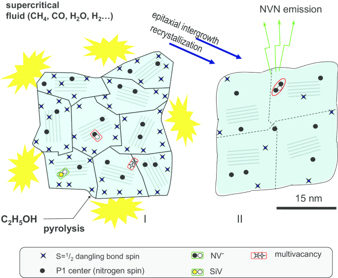
<사진>
약 30nm 크기의 서브마이크론 다이아몬드 나노결정을 생성하기 위해 고압 및 고온 조건에서 다결정 다이아몬드 입자를 소결하는 개략도. HPHT 소결 후 다결정(I)과 나노결정 모두에서 다양한 결함과 색상 중심이 관찰됩니다.
방법
샘플 제작
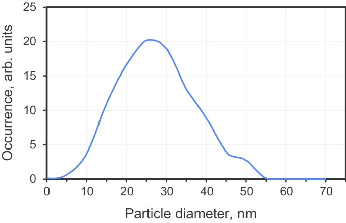
서브마이크론 다이아몬드 결정은 평균 크기가 25nm인 상업적으로 이용 가능한 전구체 다결정질 나노다이아몬드를 소결하여 제조되었습니다(제품 DP 0–0.05, Microdiamant, Switzerland). 전구체 입자는 충격파에 의해 유도된 흑연에서 다이아몬드로의 빠른 전환이 일어나는 폭발 보조 기술에 의해 얻어집니다(T에서 100마이크로초 이내에 ≈ 950°C, P ≈ 50 GPa). 폭발로 인한 제품은 다이아몬드 나노 입자 상을 정제하기 위해 화학적으로 처리되어 잔류 금속과 비정질 탄소를 제거합니다. 분말은 크기가> 10 mμ인 큰 다결정으로 구성되었습니다. 이러한 다결정은 이전에 설명된 방법[19]에 따라 결정립계를 따라 밀링 및 분해에 의해 쉽게 분획될 수 있습니다. DP 0-0.05 다결정을 형성하는 작은 크기 분획을 추출하기 위해 크기 분류가 수행되었습니다. 가장 작은 부분에 대한 결과 크기 분포(그림 2)는 최대값이 27nm이고 전체 너비 반값 최대값(FWHM) ≈ 25nm입니다(크기가 3–50nm 범위인 입자의 95% 포함). 선택된 전구체 입자는 소결을 위해 환상형 고압 챔버의 내부 흑연 실린더로 이송됩니다. 고압 챔버 내부의 일반적인 크기(즉, 위에서 언급한 두 개의 흑연 캡이 있는 중공 흑연 실린더)는 내경 4.0mm 및 높이 5.5mm입니다. 소결 전에 입자간 공간(약 30-50wt%)을 완전히 채울 때까지 건조 나노다이아몬드 분말에 에탄올을 적가했습니다[18]. 그런 다음 소결은 고압(7 GPa) 및 고온 조건(1300 ± 50 °C)에서 10초 동안 진행되었습니다. 원 프레스 실행 동안 약 ~ 120mg의 전구체 다이아몬드 분말을 처리할 수 있습니다. 고압 챔버의 구조는 Ref. [11].
<그림>
차동 원심 침강 장치(CPS 디스크 원심 분리기, CPS Instruments Inc., USA)로 측정한 평균 크기가 ~ 27 nm인 DP 0–0.05 다결정 다이아몬드 분획의 크기 분포
이 소결 과정의 효과는 그림 1에 나와 있습니다. HPHT 조건에서 소결할 때 에탄올은 초임계 상태입니다. 따라서 다결정 입자 경계에 쉽게 침투하여 다이아몬드 재결정화 및 새로운 다이아몬드 상 성장을 촉진할 수 있습니다. 소결 후, ~ 90–100 mg의 허용 가능한 품질의 백색 다이아몬드 분말(흑연 용기의 오염 없음)이 고압 챔버(여기서 D19로 표시됨)에서 추출되었습니다. 소결 후 전구체의 회색/검정색에서 흰색으로의 분말 색상 변화는 다결정 표면의 변화와 이에 상응하는 성장을 나타냅니다[11].
소결 전후 재료의 구조적 특성
다결정 나노다이아몬드 전구체의 구조적 특성화
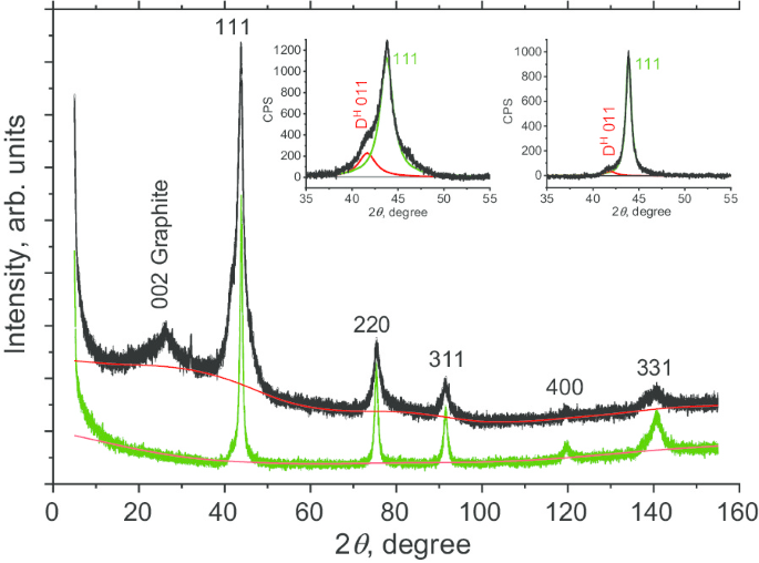
우리는 먼저 소결 전에 DP 0-0.05의 구조를 특성화했습니다. X선 회절(XRD) 측정은 CuKα 방사선(λ =1.54178 Å). 40kV 전압, 30mA 전류 및 0.1도/분의 스캔 속도가 사용되었습니다. DP 0–0.05의 XRD 패턴은 2θ에 대한 그림 3(검정색)에 나와 있습니다. 6°에서 155° 범위에서. 우리는 6개의 피크를 관찰하며 그 중 5개(111, 220, 311, 400 및 331)는 탄소의 다이아몬드 상의 특징입니다. 가장 강하게 관찰된 피크는 큐빅 다이아몬드(D
c
) 2θ에서 111 ≈ 43.7°. 이 피크는 대칭이 아니며 왼쪽 어깨를 나타냅니다. 두 개의 Lorentzian으로 패턴을 맞추면 2θ를 중심으로 한 첫 번째 피크가 생성됩니다. =43.76° 및 2θ에서 1초 =41.64°. 첫 번째 피크는 (111) 다이아몬드 평면의 반사에 해당하는 반면 두 번째 피크는 D
H
로 표시됩니다. 011) 잠정적으로:(a) 육각형 6H 다형 다이아몬드 상의 평면으로부터의 반사[20] 또는 (b) 높은 응력 하에서 결정자 사이의 다중 적층 결함, 쌍 및 관련 입자 경계에 기인합니다. D
H
의 적분을 비교하여 011 및 D
c
111개의 피크에서 DP 0–0.05 전구체에서 확인되지 않은 "상"(육각형 또는 구조적 결함으로 구성됨)이 ≈ 20wt%를 나타내는 것으로 추정됩니다. 002 Graphite로 표시된 피크(2θ에서 ≈ 26°)는 나노그라파이트 상으로 인한 것입니다. 이 불순물 상은 쉽게 제거할 수 있지만 이 연구에서는 의도적으로 산으로 에칭하지 않았습니다. 002 및 111 피크의 면적을 비교함으로써, 이 비정질 상은 ~ 4 wt% 기여하는 것으로 평가되었습니다. 그런 다음 간섭성 산란 영역 길이(LCSR ) Scherer 방법을 사용합니다. 우리는 FWHM β를 고려했습니다. sec θ의 함수로 5개의 다이아몬드 피크 중 . Β 회절계 응답 함수의 디콘볼루션 후에 결정됩니다.
각주 1엘CSR DP 0–0.05 샘플의 경우 6.7nm로 확인되었습니다.
<사진>
다결정 다이아몬드 입자의 DP 0–0.05 분획(검은색 곡선)과 소결로 얻은 D19 나노다이아몬드(녹색 곡선)의 분말 XRD 프로파일. 삽입:41.5°(D
H
)를 중심으로 하는 두 개의(빨간색 및 녹색) 로렌츠 곡선이 있는 평면(111)의 가장 강렬한 반사 피팅 011) 및 43.8
o
(D
c
111) 샘플의 경우(왼쪽 삽입) 및 소결 후(오른쪽 삽입)
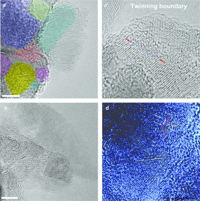
복잡한 전구체 DP 0-0.05 다이아몬드 다결정 구조에 대한 추가 통찰력을 얻기 위해 고해상도 투과 전자 현미경(HRTEM, CEOS Cs 교정기가 장착된 JEOL JEM-2100F, Shinshu University)을 사용했습니다. HRTEM은 조사 손상을 최소화하기 위해 80kV에서 작동되었습니다. HRTEM 이미지(그림 4)는 다결정이 특성이 1.93Å d인 단단히 결합된 입방형 나노다이아몬드 결정자로 구성되어 있음을 보여줍니다. - 간격 프린지. 그림 4a에서 이미지화된 다결정은 크기가 5~12nm인 결정자로 구성되어 있으며 다른 색상으로 표시된 방향이 다릅니다. 또한, HRTEM은 DP 0–0.05 분말을 구성하는 개별 다결정의 크기가 5–50 nm 범위에서 광범위하게 분포되어 있음을 보여줍니다. HRTEM 이미지는 육각형 다이아몬드 나노상(론스달라이트와 같은)의 흔적을 나타내지 않았습니다. 그러나 우리는 많은 짧은 쌍정 경계(그림 4c, d)를 관찰하며, 그 중 일부는 그림 4d와 같이 아코디언 모양의 주름진 격자 평면을 나타냅니다. 이러한 관찰은 이전에 논의된 111 XRD 피크 숄더(그림 3)가 육각형 다이아몬드 상의 존재보다는 다중 쌍정 관련 결정립계와 관련된 적층 결함으로 인한 것일 가능성이 가장 높다는 것을 나타냅니다[16].
<사진>
DP 0–0.05 분말(a , b ) 및 샘플에서 가끔 발견되는 길이가 수 나노미터인 단순 쌍정 경계의 일반적인 이미지(c , d ). 패널(a , b ):스케일 바 - 4nm. 다른 결정은 (a ). 패널의 화살표(c ) 및 (d ) 선택한 명확하게 구별되는 자매결연 경계를 표시합니다.
DP 0–0.05의 원소 조성은 유기 원소 분석 시스템(JM10, J-Science Lab Co., Ltd, Kyoto, Japan)을 사용하는 Pregl-Dumas 방법으로 분석되었으며, 이 시스템에서는 시료가 1007 °C의 온도에서 연소되었습니다. 산소 흐름(30ml/분). 산소 분율은 저울에 의해 결정되었습니다. 분석 결과(중량%)는 C-90.45, N-2.47, H-0.76, O-6.32입니다. 질소 농도가 상대적으로 높다는 것은 거의 모든 질소가 다결정 내부에 응집된 형태로, 아마도 A-센터(NN-이량체) 형태로 존재한다는 것을 의미합니다. X선 형광에 의한 추가 분석은 DP 0–0.05에서 Fe(~ 300ppm), Cu(35ppm), Si(120ppm), Cr(~ 150ppm), Ca(~ 45)의 다른 미량 원소의 존재를 보여주었습니다. ppm), Mn(45ppm), P(30ppm), Al(18ppm), Ti(13ppm), Mg(6ppm), Ni(2ppm), Zn(2ppm), Co(1ppm) .
후속 자기 공명 연구에 사용된 DP 0–0.05 샘플은 강자성 금속(주로 철 및 크롬)의 존재를 ~ 10ppm 수준으로 줄이기 위해 끓는 염산에서 추가로 처리되었습니다.
소결 다이아몬드의 구조적 특성
우리는 또한 DP 0-0.05를 소결하여 얻은 샘플 D19를 유사하게 특성화했습니다. D19 XRD 패턴은 DP 0-0.05 분말과 동일한 방법으로 얻었다. 111, 220, 311, 400 및 331 평면에 해당하는 입방 다이아몬드 상의 특징인 5개의 Lorentzian 피크(그림 3, 녹색 선)만 표시하는 것으로 나타났습니다. 전구체 물질에 흑연 상이 존재한다는 증거는 없습니다. 111 피크 비대칭도 크게 감소했습니다(그림 3, 오른쪽 삽입). 이는 적층 결함의 상당한 감소를 의미합니다. 또한 LCSR 간섭성 길이는 10.8nm인 것으로 밝혀졌으며, 이는 소결 중 다이아몬드 나노결정의 확대를 나타냅니다. 이러한 관찰을 고려하여 흑연 및 비입방 다이아몬드 상이 소결 과정에서 입방 다이아몬드 상으로 전환된다고 가정합니다. 이것은 아마도 다결정의 결정자 사이의 틈새 공간 내에서 입방형 다이아몬드 상의 성장이 뒤따르는 이 상의 용해로 인한 결과일 것입니다. 이러한 과정은 폭발 나노다이아몬드에 대해 이전에 관찰되었습니다[14].
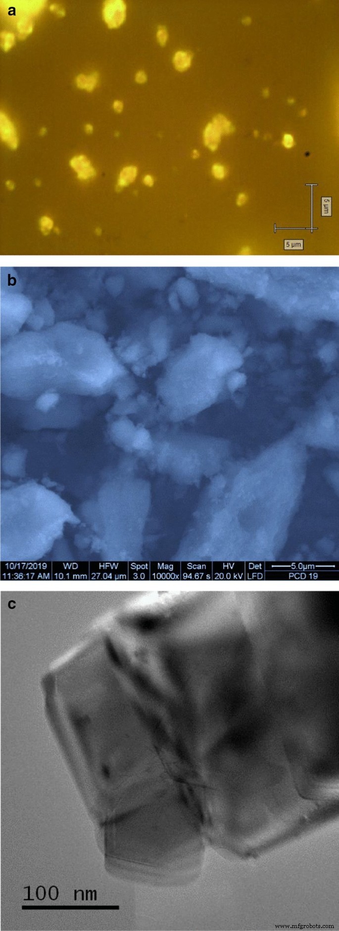
D19 샘플의 광학 및 주사 전자 현미경 이미지는 각각 그림 5a, b에 나와 있습니다. 여기에서 크기가 ~ ~ ~ 5 미크론인 임의의 모양의 입자를 볼 수 있습니다. 그들은 실제로 공유 결합이나 약한 반 데르 발스 결합으로 결합된 훨씬 더 작은 다이아몬드 결정의 조밀한 서브미크론 및 매우 느슨한 미크론 크기의 집합체입니다. 이러한 결합은 일반적으로 인접한 다이아몬드 입자의 표면 작용기의 상호작용으로 인해 발생합니다. 이러한 느슨한 집합체를 구성하는 개별 다이아몬드 입자는 투과 전자 현미경으로 볼 수 있습니다. 약 ~ 100 nm 크기의 D19 다이아몬드 결정자의 TEM 이미지가 그림 5c에 나와 있습니다. 이 이미지는 200kV의 가속 전압에서 JEOL JEM-2100F 투과 전자 현미경(Hosei University)을 사용하여 촬영되었습니다. 샘플은 탄소 기질이 없는 구리 그리드에 고정되었습니다.
<그림>
광학(a ), 주사 전자 현미경(b ) 및 투과 전자 현미경(c ) 합성된 D19 다이아몬드 입자의 이미지. 광학 이미지는 100배 현미경 대물렌즈로 촬영되었습니다. 전자 SEM 이미지를 촬영하는 데 사용되는 해당 매개변수는 패널 하단에 표시됩니다(b )
소결 전 및 후 나노다이아몬드의 결함 내용 분석 방법
두 다이아몬드 샘플 모두 EPR, 라만 및 형광 분광법으로 분석되었습니다. EPR 스펙트럼은 EPR 분광계(JES-FA 300, JEOL, Japan)를 사용하여 9.444GHz의 마이크로파 주파수에서 실온에서 기록되었습니다. 직경 4mm의 석영 EPR 튜브에 20mg의 분말 덩어리를 도입했습니다. 튜브의 분말 기둥 높이는 10mm를 초과하지 않았습니다. 튜브의 열린 끝은 습기에 대해 밀봉되었습니다.
g가 있는 EPR 스펙트럼 - g 범위의 요소 =4.00–4.30은 P의 마이크로파 전력으로 기록되었습니다. MW =10mW, 자기장 변조 진폭 Am =1mT 및 주파수 ν =100kHz, 증폭기 이득 G ≈ 10
3
, 및 N =16 신호 축적 사이클. 이러한 매개변수는 최적의 신호 대 잡음비를 얻기 위해 선택되었습니다. 시간 상수는 0.03초이고 130~200mT 간격에 걸쳐 자기장 스위프의 총 기록 시간은 120초였습니다. g가 있는 EPR 스펙트럼 -요소 g ≈ 2는 P의 마이크로파 전력으로 327~347mT의 간격으로 기록되었습니다. MW =0.03mW, 자기장 변조 진폭 Am =0.035mT, 증폭기 이득 G ≈ 10
2
, 및 N =4 신호 축적 사이클. 일반적으로 광범위한 주요 EPR 신호(g ≈ 2) 선폭> 0.5 mT, 피크 대 피크 EPR 신호 강도(Ipp ) MW 전력 의존성을 따릅니다. Ipp ~ (피MW )
1/2
최대 PMW ≈ 100mW. 반면에 좁은 EPR 신호(저전력에서 선폭 <0.15mT)의 경우 IppP에서 포화 MW> 0.05mW이고 더 높은 값(> 4mW)에서 강한 모양 왜곡이 있습니다. 이러한 포화 경향은 다결정 전구체와 이후 소결된 다이아몬드 모두에서 관찰되었습니다.
우리는 50배 대물렌즈(NA =0.78) 및 CCD를 사용하는 광학 현미경(독일 라이카)과 함께 마이크로 라만 분광계("inVia", Renishaw, UK)를 사용하여 광발광(PL) 및 라만 스펙트럼을 획득했습니다. 후방 산란 기하학에서 -70°C로 냉각된 검출기 스펙트럼은 ~ 2cm
–1
의 스펙트럼 분해능으로 기록되었습니다. . 강도가 20Wcm
−2
미만인 488nm 및 457nm 파장에서 아르곤 이온 레이저의 두 레이저 라인을 사용했습니다. 샘플의 초점에서. 마이크론 크기의 원에 대한 표준 초점과 비교하여 2 × 30 mμ 스트라이프에 초점을 맞추기 때문에 샘플 평면에서 더 낮은 여기 레이저 강도를 사용하는 StreamLine™ Plus(Renishaw, UK) 모드에서 스펙트럼 이미지를 기록했습니다. 이 전략은 주변 대기에서 과열 및 산화를 통한 레이저 유도 샘플 손상 및 국부 기상 에칭을 제한했습니다. 이 기술과 직경 2mm의 실린더에서 다이아몬드 분말 압축에 대한 자세한 내용은 이전에 설명되었습니다[19].
분리된 D19 입자의 형광 이미지는 100X 대물렌즈를 사용하여 공초점 광시야 형광 현미경으로 얻었다. 스핀 코팅을 통해 D19 분말의 희석된 수성 현탁액의 상층액 분획으로부터 입자를 유리 커버슬립에 침착시켰다. 커버슬립은 잔류 유기물로부터의 기생 형광을 방지하고 커버 유리에 D19 입자의 더 나은 부착을 촉진하기 위해 산소 플라즈마에서 미리 처리되었습니다. 형광은 488nm 레이저(여기 전력 ≈ 40mW)로 여기되고 525/40 간섭 필터로 수집되었습니다. 특별히 냉각된 2D 어레이 CCD 검출기(카메라 온도 =− 79.9 °C)를 사용하여 이미지를 기록했습니다. 이미지(크기 ~ 80 × 80μm, 80.00nm/픽셀)는 60ms 노출 시간으로 기록되었습니다. 이미지 프레젠테이션에는 그레이스케일 팔레트가 사용되었습니다. 이미지는 피지 소프트웨어를 사용하여 분석되었습니다.
<섹션 데이터-제목="결과">
결과
소결 전후의 다결정 및 다이아몬드 결정의 EPR
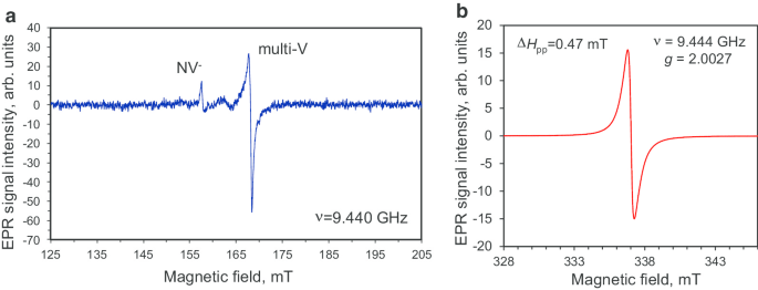
반자계 범위와 높은 자기장 범위 모두에서 DP 0–0.05 다결정 다이아몬드 분말의 EPR 스펙트럼이 그림 6에 나와 있습니다. 이러한 별개의 범위에 등록된 EPR 스펙트럼은 높고 낮은 마이크로파에서 측정되었습니다. 힘 PMW =10mW 및 PMW =0.03 mW, 각각. 여기에서 하이필드 영역은 일반적으로 메인 마이크로파 유도 플립플롭 ΔM과 관련된 흡수선 부근에서 선택되었습니다. s =1 회전 전환 S =½인 반면 확장된 반장 범위는 ΔM의 신호를 검색하기 위해 특별히 선택되었습니다. s =가능한 삼중항 S의 2 전환 =1 센터. 하프필드 EPR 스펙트럼은 강도가 매우 낮고 삼중항 NV
-
의 존재를 보여줍니다. 센터(g로 신호 =4.27 at Hres =158 mT [10, 16]) 및 삼중항 다중 공석(g이 있는 신호 =4.00, Hres =168 mT[16]) 다결정 다이아몬드 전구체에서. 이 두 가지 결함 유형은 모두 매우 작은 농도(<1 ppm)로 존재합니다. 따라서 그러한 희귀한 중심을 탐지하기 위해 높은 마이크로파 전력을 사용할 필요가 있었습니다. 더욱이, 고장 영역에서 우리는 또한 스핀-하프 센터의 특징적인 서명을 관찰했습니다(g =2.0027 at Hres =337 mT [10, 16, 21]), 그러나 폭이 넓음(ΔHpp =0.47 mT), 미세 구조가 없는 단일 Lorentzian 파생 모양[16]. 이러한 스핀이 독립적인 중심에서 나온다는 가정을 감안할 때, 이 광범위하고 강렬한 신호는 잠정적으로 C–C 댕글링 본드 스핀과 결합된 상자성 질소 스핀을 해결되지 않은 초미세 구조(HFS)로 교환하기 때문일 수 있습니다.
각주 2
스핀 S로 모든 상자성 종의 농도를 추정했습니다. =1/2은 ~ 4 × 10
19
입니다. 스핀/g(800ppm), 이는 이전에 5nm 폭발 나노다이아몬드에 대해 보고된 값보다 ~ 1.5배 작습니다[22].
<그림>
반 자기장 범위에서 다이아몬드 입자의 DP 0–0.05 분율의 EPR 스펙트럼(a ) 및 g에서 강한 신호를 갖는 단일항의 공진 자기장 주변 -요소 g ≈ 2.0027(b ). 전자레인지 PMW :10mW(a ) 및 0.03mW(b ). 마이크로파 주파수 ν =9.44GHz. 두 스펙트럼 모두 포화에서 멀리 떨어진 영역에 등록됩니다.
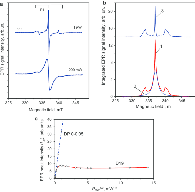
그림 7a는 D19 샘플의 EPR 스펙트럼이 매우 낮음(PMW =1μW) 및 매우 높은(200mW) 마이크로웨이브 전력, i.e. 포화 상태보다 훨씬 낮은 영역 또는 포화 상태(확대에 의해 입증됨)에서 각각. P 스펙트럼 MW =1 Wμ는 전구체 입자에 비해 0.14mT의 좁은 선폭을 갖는 중심선을 갖는다. 그림 7b(곡선 1)는 이중 통합된 낮은 마이크로파 전력 EPR 신호를 표시합니다. 이 신호는 다음과 같이 분해될 수 있습니다. 가장 풍부한 S와 관련된 넓은(FWHM ≈ 1.7 mT) 로렌츠 모양 신호(그림 7b, 곡선 2) =~ 6 mT로 분리된 두 개의 대칭 위성 라인이 있는 매우 좁은 중심선과 ~ 6 mT(그림 7b, 곡선 3). 중심선에 대한 두 위성선의 적분강도비는 각각 0.90과 1.09이다. 따라서 ± 10% 실험 측정 정확도 내에서 동일한 통합 강도를 갖습니다. 위성 라인은 중성 상자성 치환 질소의 EPR 신호의 초미세 구조와 관련이 있습니다(
14
N, S =1/2, 나 =1), P1 중심[23, 24]으로 알려져 있습니다. P1 중심은 전구체 다결정 나노다이아몬드에서 관찰되지 않았지만 소결 후에 다이아몬드에서 명확하게 검출되었다. 이전 연구에서는 P1 중심과 관련된 이 특징적인 삼중항 HFS 구조가 50–80 nm를 초과하는 크기를 가진 거친 다이아몬드 결정에서만 나타나는 것으로 나타났습니다[25]. 더욱이, 에탄올 존재하에서 폭발 나노다이아몬드의 소결은 다이아몬드 재결정화 및 새로운 다이아몬드 상 성장에 기초한 결정자 확대를 촉진하는 것으로 입증되었다[26]. 따라서 현재 EPR 데이터는 크기가 ~ -10nm인 다결정 입자의 개별 결정자에서 개별 크기가 40-50nm인 새로운 결정자까지 여기에서 발생하는 유사한 확대와 일치합니다.
각주 3
<그림>
낮고 높은 마이크로파 전력에서 D19 다이아몬드 결정의 주요 첫 번째 파생 EPR 신호(a ), 통합된 EPR 신호를 두 그룹의 스핀과 관련된 구성 요소로 분해(b ) 및 최대 200mW 범위에서 이 EPR 신호의 피크 강도 대 마이크로파 전력의 제곱근의 해당 포화 추세(c ). P1 중심의 EPR 신호(치환 질소)의 삼중항 HFS 구조는 (a ). (b에서 ):삼중항 구조를 갖는 곡선 3은 P1 중심의 EPR 스펙트럼에만 해당합니다. (c에서 ):파선 직선은 Ipp 대 (PMW )
1/2
참조용으로 제공된 DP 0–0.05 다결정에 대한 의존성. P에서 4개의 실험 지점 MW =0.5, 1, 2, 4 mW가 플로팅에 사용되었습니다(그 중 2개는 여기에 표시되지 않음). 마이크로파 주파수 ν =9.44GHz
이 가설은 좁은 EPR 신호의 관찰에 의해서만 확인되는 것이 아닙니다
각주 4
(지 =2.0024) HFS 특성을 갖는 P1 센터의 [26] 뿐만 아니라 I의 검출에 의해 ppP 이상의 채도 MW =D19 샘플의 경우 0.7 mW. 전구체 다결정 나노다이아몬드 DP 0–0.05의 경우 높은 수준의 마이크로파 전력(P)에서도 주요 EPR 신호의 피크 강도가 포화되지 않습니다. MW =20mW). 전력 의존 나pp ~ (피MW )
1/2
마이크로파 전력의 전체 범위에서 잘 유지됩니다(PMW =0–20mW). 나pp ~ (피MW )
1/2
DP 0–0.05 샘플에 대한 의존성은 최대 ~ 16mW 마이크로파 전력까지 점선으로 그림 7c에 표시됩니다. 포화가 없는 이러한 선형 의존성은 다결정 나노다이아몬드 내의 상자성 중심의 높은 농도와 매우 짧은 스핀-격자 및 스핀-스핀 이완 시간으로 인한 것입니다. D19 샘플 g의 포화 거동 =2.0024 EPR 신호는 0–200mW 범위의 그림 7c에도 표시됩니다.
각주 5
우리는 나를 관찰합니다. pp ~ (피MW )
1/2
~ 15 Wμ 미만의 마이크로파 전력에만 의존합니다. 이 경우, 나pp 1 mW 미만 범위에서 포화를 나타내고 ~ 1 mW에서 최대값에 도달합니다. 나pp 그런 다음 사용된 최대 전력(200mW)까지 천천히 다시 증가하기 전에 1–25mW 범위에서 상당히 감소합니다. I에서 이러한 포화 경향의 존재 pp (피MW ) 및 P 위의 드롭 MW =1 mW는 다른 결함과 입자 가장자리에서 멀리 떨어진 상대적으로 큰 스핀-스핀 및 스핀-격자 이완 시간을 갖는 P1 중심의 특성입니다[27]. 이러한 조건은 크기가 60~80nm를 초과하는 Ib형 HPHT 나노다이아몬드에서 200ppm보다 작은 P1 중심 농도에 대해 충족됩니다. 그러나 EPR의 관점에서만 볼 때 개별 D19 다이아몬드 결정자(원소 입자)의 실제 평균 크기는 미해결 문제입니다. D19의 실제 EPR 스펙트럼을 평균 크기가 18~390nm인 밀링된 Ib HPHT 다이아몬드의 일련의 분말 EPR 스펙트럼과 비교하여 대략적으로 해결할 수 있습니다[28]. Ref. [28], 이러한 EPR 스펙트럼이 발표된 곳에서 치환 질소와 관련된 P1 HFS 서명은 평균 크기가 ≤ 30 nm인 분말 다이아몬드에는 완전히 존재하지 않지만 중간 크기(85–130 nm)의 샘플에는 여전히 존재합니다. 이 비교는 합성된 D19 다이아몬드 결정자의 평균 크기가 10,030 ± nm 영역에 있음을 나타냅니다. This estimation coincides well with the representative size observed in the TEM image shown in Fig. 5c. It is notable that the EPR spectrum of D19 recorded at the high power of PMW = 200 mW (Fig. 7a) shows a lack of definition of the HFS structure of the P1 signal. The broad central line suggests the presence, at the nanoscale, of dense clusters of paramagnetic spin-half that strongly couple to each other.
Altogether, the decrease in the linewidth of the main EPR signal (g = 2.0024), the appearance of well-defined HFS characteristics in the P1 centre spectrum after sintering, and the Ipp saturation for PMW > 0.7 mW (Fig. 7c) are suggestive of an increase in size by up to one order of magnitude (crystal size > 50 nm). It also indicates a better crystallinity of the nanodiamond in the D19 sample. From van Wyk measurements [29], a smaller amount of paramagnetic defects (< 200 ppm) are expected, based on the narrow linewidth (0.14 mT) of the g = 2.0024 main paramagnetic signal in the D19 sample.
Fluorescence and Raman Scattering of Diamond Crystals
The photoluminescence (PL) spectrum of the DP 0–0.05 precursor together with the PL spectra of some much coarser fractions of polycrystalline diamond particles (DP 0–0.2 and DP 0–0.35) produced by Microdiamant
TM
is shown in Fig. 8. The spectrum of DP 0–0.05 under the 488 nm excitation wavelength has two features of note:the prominent narrow PL line at 738 nm, associated with the zero-phonon line of negatively charged SiV
−
centres, and a broad spectrum background with PL bands centred at 525, 600, 660 and 740 nm, associated with various light-emitting centres in diamond, including NV centres. For polycrystals with mean size 25 nm (DP 0–0.05), the intensities of these bands are smaller than that for polycrystals with mean sizes of 100 and 175 nm (DP 0–0.2 and DP 0–0.35, respectively). A more detailed analysis of the PL spectra of polycrystalline DP 0–0.05 particles has been previously undertaken [19].
PL spectra of various submicron fractions of Microdiamant™ polycrystalline diamond particles:blue—DP 0–0.05 (mean size 25 nm), green—DP 0–0.2 (mean size 100 nm), red—DP 0–0.35 (mean size 175 nm). Excitation wavelength λ = 488 nm. The prominent peak at 738 nm marked by the vertical dashed line is the zero-phonon line of negatively charged SiV
−
centres, which can be observed in all polycrystalline diamond fractions. For better comparison, the spectra are specially normalized for PL intensity at λ = 590 nm. Normalising coefficients are indicated in the figure
Figure 9a shows the PL spectrum of sintered diamond sample D19 (blue curve) at room temperature (RT) together with the PL spectrum of the DP 0–0.05 precursor (red curve). The D19 spectrum displays a green fluorescence characteristic, with a sharp maximum at 525 nm, and a subsequent decrease at larger wavelengths. Note that the single-phonon, sharp Raman line of diamond, which is expected at 522 nm, was too weak to be detected on the ascending slope of the PL signal under 488 nm excitation wavelength.
Footnote 6
As previously reported [9, 30], such spectra—with a continuous higher wavelength band of “triangular” shape—are characteristic of optical emission from NVN centres (also known as H3 centres) in submicron (< 140 nm) diamonds at RT. In the PL spectrum of sample D19, at least four broad bands (“bumps”) centred at 538, 569, 601 and 710 nm can be additionally distinguished. We do not believe that they are related to phonon sidebands of the NVN (H3) centres. The origin of the 525 nm sharp peak and “bumps” is still unclear, but it is probably due to an impurity-related complex; the precursor material contains a large number of residual contaminants as mentioned before (see “Structural Characterisation of the Materials Before and After the Sintering” section), some of which are present at significant concentrations (~ 100 ppm). The zero-phonon emission line of NVN at ~ 503 nm wavelength is barely detectable and cannot be distinguished from the two small shoulders (at 500 and 505 nm) in the same region. By comparing the D19 and DP 0–0.05 spectra (Fig. 9a), one can see that they superimpose well for λ > 750 nm. However, the spectra differ significantly in the 480–650 nm range due to the appearance after sintering of NVN centres, which were not present in the precursor material. In order to verify our interpretation of the main optical emission of D19 (in the range 500–650 nm) as originating from NVN centres, we compared the PL spectrum of D19 with the PL spectra of two reference samples (HPHT diamonds, Columbus NanoWorks Inc., US) of two very different sizes and both known to contain NVNs (Fig. 9b). The D19 PL spectrum (dashed line) coincides very well with those of the PL spectra of the HPHT microdiamonds containing NVNs. The emission spectrum of the 100-µm sized reference sample shows a sharp single-phonon diamond Raman line (487.4 nm) and the zero-phonon line (504 nm) of NVN under 457 nm laser excitation at room temperature (Fig. 9b, violet spectrum). The 150-nm sized HPHT nanodiamonds were excited at 488 nm, and it displayed a very similar global photoluminescence spectrum shape as that of the 100-µm sized sample, with a Raman single-phonon line at 522 nm. However, it did not exhibit the NVN zero-phonon line, behaving in that sense exactly like the D19 sample. The “bumps” present in the D19 sample spectrum are absent from both reference PL spectra, indicating that these features are not related to the NVN emission.
PL spectrum of submicron powder D19 sample at T = 293 K (blue line) compared with that of its DP 0–0.05 polycrystalline precursor (red line) under the same conditions with laser excitation at λ = 488 nm (a ), emission spectra, under 457 nm and 488 nm excitation, of two reference synthetic HPHT samples (size ~ 100 μm and < 150 nm) containing NVN centres (b ) and the Raman spectrum of D19 sample recorded using the 457 nm excitation laser radiation (c ). Arrows in (b ):lines at 487.4 nm and 522 nm are single-phonon diamond Raman lines at 457 nm and 488 nm excitation, respectively, and the line at 504 nm is the ZPL of the NVN centres. In (b):dashed line—PL spectrum of D19 at λ = 488 nm excitation (for comparison). In (c ):the diamond Raman line is centred at 1331.4 cm
−1
. δ = 7.3 cm
−1
is a FWHM of diamond Raman line having the Lorentzian shape
We also measured Raman scattering from D19, in the range 1000–1600 cm
−1
, under excitation by 457 nm laser radiation. Figure 9c displays the Raman spectrum, corrected to remove the autofluorescence background. The spectrum consists primarily of a narrow characteristic diamond Raman line centred at 1331.4 cm
−1
and an exceptionally broad (width ≈ 100 cm
−1
) band centred at 1450 cm
−1
. The latter could be due to non-diamond amorphous carbon phase and/or some transpolyacetylene (TPA) species located at diamond crystals surface [1,2,3]. A further, ill-defined, band at ~ 1090 cm
−1
of lower intensity is probably related to TPA species. The broad band at ~ 1450–1480 cm
−1
could also be related to multivacancy chains in the diamond lattice and sp
2
- rehybridisation within these chains [6].
Footnote 7
Furthermore, we did not observe the characteristic G-band (centred at 1570–1590 cm
−1
) associated with an sp2
graphitic nanophase. These observations are indicative that the diamond sample D19 being graphite free, which is also in agreement with its white colour under daylight illumination.
Moreover, the width of the Raman diamond line (7.3 cm
−1
) in the D19 sample is smaller than that for the DP 0–0.05 polycrystalline particles (10.6 cm
−1
). Table 1 contains Raman diamond line data for bead-milled synthetic Ib HPHT diamonds with mean size varying from 25 to 1000 nm (Microdiamant AG, Switzerland). The linewidth decreases from 9.12 to 5.24 cm
−1
with increasing size. This can be explained by the lower prevalence of structural defects in larger crystals. Using data as a calibration curve to infer the crystal size from the diamond Raman linewidth of δ ≈ 7.3 cm
−1
yields an estimation for the D19 crystal size of ~ 80 nm. This value coincides reasonably with the estimation in “EPR of Polycrystals and Diamond Crystallites Before and After the Sintering” section on the basis of EPR data. Moreover, this value is very similar to our previous published results where diamonds were obtained by HPHT sintering of 5-nm DND in the presence of ethanol [31]. However, the precursor material used for sintered DND and the one used in this work using the smallest (~ 25 nm) fraction of milled Du Pont shock-wave polycrystalline diamonds are considerably different from the viewpoint of crystal types and elementary crystallite sizes. This obtained size is about 8 times larger than the coherent scattering region length of LCSR ≈ 11 nm extracted from XRD earlier, but it is consistent with crystallite having a low density of structural defects, in agreement with the EPR studies.
We also studied the fluorescence from very fine individual D19 particles. For this purpose, the supernatant fraction of diluted and ultrasonicated water suspension of D19 particles obtained after centrifugation at 4500 × g for a 30 min was used. Coarse particles and large loose aggregates with size exceeding ~ 0.2–0.3 micron were absent in such supernatant. Fine D19 particles were spin-coated onto a thin glass coverslip from the diluted supernatant of D19 particles. A typical image of fine fluorescent D19 particles is shown in Fig. 10a in greyscale (mono 14-bit images). It consists of many spots with different brightness. Some spots, such as that marked by the yellow circle, have sizes close to the diffraction limit. The intensity profile of this spot has a Gaussian shape in its central core and a FWHM of about 5–6 pixel corresponding to ~ 440 nm (Fig. 10b). Such spots come from at least quarter-micron particles and particles of smaller size. A greater number of brighter spots correspond to the larger reassembled aggregates of D19 particles having more NVN colour centres and hence the overall emission intensity increasing.
Wide-field fluorescent image of isolated D19 particles obtained by confocal epifluorescence microscopy (a ), and the intensity profile of the selected nanoparticle marked by the yellow circle (b ). Image size: ~ 80 × 80 mμ. One pixel corresponds to 80 nm
Discussion
We showed that under HPHT conditions, and in the presence of ethanol, we can convert polycrystalline diamond particles (composed of tightly cemented nanometre-sized cubic diamond crystallites separated by a non-cubic diamond phase) into larger cubic diamond crystallites. The process probably occurs through recrystallisation of the cubic diamond phase and transformation of non-cubic diamond phases including multiple twin boundaries into diamond. During this process, vacancies appear and can form NVN complexes with nitrogen atom pairs. These complexes have a characteristic photoluminescence in the green. While the EPR spectra of the precursor polycrystalline diamonds show NV
−
triplet centres, triplet multivacancies, and SiV
−
centres, none of these were present after the sintering. The disappearance of NV
−
centres and multivacancies has previously been observed [31] after sintering detonation nanodiamonds at HPHT conditions (P = 7 GPa and T ≥ 1350 °C) with ethanol.
Footnote 8
The presence of multivacancies is a characteristic feature of damaged diamond lattices, with defects mainly located in a thin layer of ~ 2 nm at the surface. The absence of the paramagnetic triplet and SiV colour centres is strong evidence that substantial recrystallisation took place, accompanied with the appearance of new defect types (NVN). The saturation trend of the substitutional nitrogen (P1 centre) EPR signal with increasing microwave power indicates long spin–spin and spin–lattice relaxation times. These are signatures of improvement of the quality of diamond crystal lattice after sintering. We can assume that during HPHT sintering, vacancies from empty spaces within or between polycrystals join with A-centres to form the new NVN entities.
결론
Sintering of diamond polycrystals, with size varying from 3 to 50 nm, in the presence of ethanol, lead to the substantial enlargement of elementary diamond nanocrystals and improved their crystalline quality. During this process, SiV
−
and NV
−
colour centres present in the precursor nanodiamond disappeared, while the EPR signature of P1 substitutional nitrogen paramagnetic centres appeared. We also observed the green photoluminescence of NVN colour centres. The comparison of the FWHM of diamond Raman line (~ 1332 cm
−1
) of the synthesised selected microcrystals under study with those of a series of reference samples revealed that the mean size of diamond crystals after sintering is approximately 80 nm. The analysis of the EPR spectrum dependence upon microwave power demonstrated the good crystalline quality of the synthesised sintered diamond with a concentration of P1 centres smaller than 200 ppm. Hence, our technique of HPHT sintering is a strong alternative to conventional high-energy particle beam irradiation [9] to form NVN centres in nanodiamond. It can be used to produce purely “green” fluorescing nanodiamonds with no (or very limited) crosstalk with the “red” fluorescing nanodiamonds (containing NV
0
and NV
−
centres), as required in biolabelling for cathodoluminescence integrated correlation electron-light microscopy [32].
데이터 및 자료의 가용성
The data underpinning this manuscript is available from the corresponding author on request.
Notes
1.
The apparatus response function of the XRD diffractometer was determined from a LaB6 reference sample.
2.
One mechanism explaining the lack of HFS in the EPR signal of paramagnetic nitrogen in size < 50 nm diamond nanoparticles is described in detail elsewhere [21]. Alternative mechanisms are also not excluded [33, 34].
3.
X-ray diffraction CSR size is ~ 4 times smaller in this case.
4.
This narrow EPR signal is slightly asymmetrical and consists of at least two components related to P1 centres and to defects having C–C dangling bond spins S = 1/2. The intensity of the second component represents at least 30% of the intensity of the main peak.
5.
Here we assume the sequence of untreated first-derivative experimental EPR spectra measured at different PMW , two of which are shown in Fig. 7a.
6.
However, the Raman line was detected at 457 nm excitation.
7.
The Raman band centred at ~ 1480 cm
−1
was found for HPHT diamonds grown with magnesium-based catalysts [6]. Such diamond crystals may contain SiV and GeV colour centres.
8.
Instead of a multivacancy g = 4.00 singlet EPR signal, a new EPR signal with a quintet hyperfine structure related to N⋯N pairs separated by no more than 0.7 nm was observed in this case.