

나노물질

산업 제조
AZO 전도층의 저항률이 MCP 저항 요구 사항 이내일 때 Zn 함량의 간격은 매우 좁고(70-73%) 제어하기 어렵습니다. 마이크로채널 플레이트 상의 AZO 전도층의 특성을 고려하여 전도성 물질인 ZnO와 고저항 물질인 Al2O3의 비율을 조절하는 알고리즘을 설계하였다. 우리는 MCP의 작동 저항(즉, 마이크로 채널에서 전자 눈사태 동안의 저항)의 개념을 제시합니다. AZO-ALD-MCP(Al2O3/ZnO 원자층 증착 마이크로 채널 플레이트)의 작동 저항은 MCP 저항 테스트 시스템에 의해 처음으로 측정되었습니다. 기존 MCP와 비교하여 AZO-ALD-MCP의 작동 상태와 비 작동 상태의 저항이 매우 다르며 전압이 증가함에 따라 작동 저항이 크게 감소 함을 발견했습니다. 따라서 우리는 전도층에 대한 일련의 분석 방법을 제안했습니다. 우리는 또한 작동 저항 조건에서 ALD-MCP 전도층의 전도성 물질과 고저항 물질의 비율을 조정하는 것을 제안하고 고이득 AZO-ALD-MCP를 성공적으로 준비했습니다. 이 디자인은 MCP의 성능을 향상시키기 위해 ALD-MCP의 전도층을 위한 더 나은 재료를 찾는 길을 열어줍니다.
마이크로채널 플레이트(MCP)는 얇은 유리판 형태 통합에 의한 2차원 기공 어레이로 구성된 전자 증배기입니다. 길이는 0.5~5mm, 직경은 4~40μm이며 바이어스 각도는 일반적으로 법선에 대해 5°~13°입니다. 판 표면의; 판의 개방 면적 비율은 최대 60%이며, 각 기공의 높은 길이 대 지름 비율은 약 20:1 ~ 100:1입니다[1].
그림 1과 같이 마이크로채널로 입사한 입사전자가 벽과 충돌하여 마이크로채널 벽 표면에 2차 전자가 생성된다. 마이크로 채널 벽과의 다중 충돌은 2차 전자의 수를 증가시켜 마이크로 채널 내부에 전자 사태를 일으키고 마이크로 채널의 출력에서 전자 구름을 방출합니다. 2차 전자 전자는 바이어스 전압에 의해 마이크로 채널을 따라 더 가속됩니다. MCP 이득은 10 3 입니다. –10 4 작동 전압 700–900V에서 [2,3,4,5,6,7,8,9].
<그림>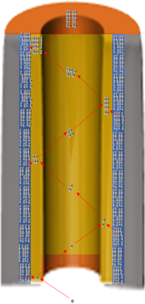
MCP 작동 상태 다이어그램
각 마이크로 채널은 검출기 및 전자 증배기 역할을 합니다. 수백만 개의 마이크로 채널이 독립적으로 작동함으로써 MCP는 광자, 전자, 중성자 및 이온을 식별하는 데 사용되는 높은 공간 분해능, 높은 타이밍 분해능 및 넓은 범위의 이득 특성을 갖습니다. MCP는 광전 검출기, 광전자 증배관(PMT), 자외선 분광계, 음극선관, 주사 전자 현미경, 전계 방출 디스플레이, 잔류 가스 분석기, 의료 영상, 비행 시간 질량 분석기, 야간을 포함한 다양한 종류의 기기에 통합할 수 있습니다. - 시력 고글 등 [1, 4, 7,8,9]. 전통적인 공정의 수소 연소는 마이크로 채널을 적절한 전도도 및 2차 전자 방출 계수로 만듭니다.
마이크로 채널을 준비하는 일반적인 수소 소성 공정에는 많은 단점이 있습니다. 첫째, 수소 소성 공정은 전도층과 발광층을 독립적으로 조정할 수 없습니다[10, 11]. 둘째, 중금속 원소(Pb, Bi)는 납 유리 제련 공정에서 환경 오염을 유발합니다. 셋째, 고온으로 인해 MCP의 넓은 영역이 뒤틀릴 것입니다[8]. 넷째, 수소 환원 반응에 사용되는 납 유리에는 K, Rb 및 기타 방사성 원소가 포함되어 배경 소음이 발생합니다[8]. 마지막으로 기공에 잔류하는 수소는 바이어스 전압에 의해 이온이 되어 전자의 반대 방향으로 날아가 기기의 음극을 파괴한다[8, 12].
초기 과학자들은 수소 연소 공정을 대체하기 위해 마이크로 채널 벽에 전도층과 발광층을 성장시키는 솔루션을 제안했습니다[3]. 많은 박막 증착 방법은 길이 대 직경 비율이 높은 마이크로 채널에서 균일한 막을 성장시킬 수 없습니다. Argonne 국립 연구소는 마이크로채널 벽에 온전하고 균일한 막을 형성하기 위해 MCP에서 전도층과 방출층을 성장시키기 위해 원자층 증착(ALD)을 사용할 것을 제안했습니다[4, 13]. 또한 ALD-MCP는 앞서 언급한 단점을 해결합니다. 많은 연구 기관은 MCP의 성능을 향상시킬 수 있는 경쟁력 있는 재료를 찾는 것을 목표로 하고 있습니다.
Argonne 국립 연구소는 MCP 저항 요구 사항을 고려하여 ALD-MCP 전도층에 AZO 재료를 선택합니다. 저항이 너무 높으면 전도층이 적시에 발광층에 전자를 보충할 수 없으며 지속적으로 MCP 게인이 낮거나 작동하지 않을 수도 있습니다. 반면에 저항이 너무 낮으면 MCP가 과열되어 결국 고장으로 이어집니다[4, 9, 14, 15]. 따라서 ALD-MCP에서는 전도층의 설계가 중요합니다.
그림 2에서 볼 수 있듯이 AZO 전도층의 저항이 MCP 저항 요구 사항 이내일 때 허용되는 Zn 함량은 매우 좁은 범위(70~73%)에 있습니다[16]. 따라서 MCP 이득이 불안정하고 MCP가 쉽게 파손될 수 있습니다. Zn 대신 W 및 Mo와 같은 대체 전도성 재료가 연구되었습니다[3, 4, 17, 18, 19]. \({\text{WF}}_{6}\) (\({\text{MoF}}_{6}\)) 및 \({\text{H}}_{2}의 화학 반응 {\text{O}}\)는 ALD에 의해 W(Mo)를 성장시키는 데 사용됩니다. 그러나 \({\text{WF}}_{6}\) 또는 \({\text{MoF}}_{6}\)를 사용하면 두 가지 심각한 단점이 있습니다. 즉, 부식성이 강하고 불순물이 포함되어 있습니다. 생산 과정에서 제거하기 어렵습니다. 이러한 이유로 이러한 재료를 사용한 ALD-MCP는 비용이 많이 듭니다.
<그림>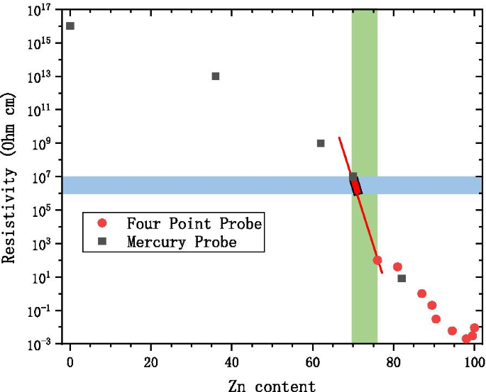
Zn 함량, Zn/(Zn + A)*100(%), 파란색 영역은 MCP 저항 영역, 녹색 영역은 AZO 변경 영역, 빨간색 영역은 제어가 필요한 영역
우리 연구에서 ZnO 및 \({\text{Al}}_{2} {\text{O}}_{3}\)를 사용한 합리적인 설계가 문제 없이 MCP 전도층에 대해 실현될 수 있음을 발견했습니다. W 또는 Mo를 사용하면 직면하고 가격 경쟁력이 있습니다. 여기에서는 AZO 전도층이 있는 ALD-MCP를 AZO-ALD-MCP로 명명합니다.
우리는 원하는 AZO 전도층 특성을 얻기 위해 전도성 물질 ZnO와 고저항 물질 \({\text{Al}}_{2} {\text{O}}_{3}\)의 비율을 조정하는 알고리즘을 제안합니다.
우리는 MCP의 작동 저항(즉, 마이크로 채널에서 전자 눈사태 동안의 저항)의 개념을 제시합니다. 우리는 AZO-ALD-MCP의 작동 저항을 테스트했으며 AZO-ALD-MCP와 기존 MCP 간의 두 가지 차이점을 발견했습니다. 우리는 AZO-ALD-MCP와 기존 MCP의 작동 및 비 작동 저항이 크게 다르다는 것을 관찰했습니다. 또한 AZO-ALD-MLP의 저항은 전압과 음의 상관 관계가 있습니다. 도전성 재료와 고저항 재료의 비율 조정에 대한 우리의 제안(작업 저항 참조)은 ALD-MCP 도전층의 성능 향상에 사용할 새로운 재료를 찾는 데 도움이 되는 지침을 제공합니다. 미래의 MCP.
ALD(Atomic Layer Deposition)는 제어된 속도로 물리적 또는 화학적 흡착 또는 표면 포화 반응을 위해 기판 표면에 전구체와 반응성 가스를 교대로 적용하는 기술입니다. 재료는 단원자 필름 표면의 형태로 기판에 증착됩니다. ALD는 pinhole이 없는 연속막을 형성할 수 있고, Coverage가 우수하며, 원자막의 두께와 조성을 조절할 수 있다[1, 2, 4, 11, 13, 19, 20].
다음은 ALD를 사용하여 Al2을 성장시키는 화학 반응식입니다. O3 :
$$\begin{정렬} &{\text{A}}:{\text{기판}} - {\text{OH}}^{*} + {\text{Al}}\left( {{\text {CH}}_{3} } \right)_{3} \\ &\quad \to {\text{기판}} - {\text{O}} - {\text{Al}}\left( { {\text{CH}}_{3} } \right)_{2}^{*} + {\text{CH}}_{4} \uparrow \\ &{\text{B}}:{\ text{기판}} - {\text{O}} - {\text{Al}}\left( {{\text{CH}}_{3} } \right)_{2}^{*} + 2 {\text{H}}_{2} {\text{O}} \\ &\quad \to {\text{기판}} - {\text{O}} - {\text{Al}}\left ( {{\text{OH}}} \right)_{2}^{*} + 2{\text{CH}}_{4} \uparrow \\ &{\text{C}}:{\text {알}} - {\text{OH}}^{*} + {\text{알}}\left( {{\text{CH}}_{3} } \right)_{3} \\ { } &\quad \to {\text{Al}} - {\text{O}} - {\text{Al}}\left( {{\text{CH}}_{3} } \right)_{ 2}^{*} + {\text{CH}}_{4} \uparrow \\ &{\text{D}}:{\text{Al}} - {\text{CH}}_{3} ^{*} + {\text{H}}_{2} {\text{O}} \to {\text{Al}} - {\text{OH}}^{*} + 2{\text{ CH}}_{4} \uparrow \\ \end{정렬}$$반응 온도는 60–150°C입니다. 그림 3과 같이 Al2의 층을 성장시키는 시간과 순서는 O3 원자는:
<그림>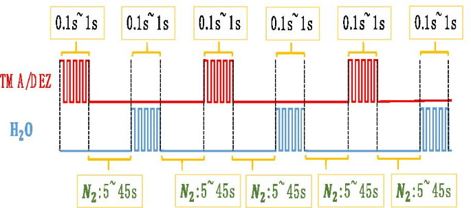
성장하는 Al2 O3 및 ZnO 다이어그램
\({\text{TMA}}/{\text{N}}_{2} /{\text{H}}_{2} {\text{O}}/{\text{N}}_{ 2} =0.1\sim1{\text{s}}/5\sim45{\text{s}}/0.1\sim1{\text{s}}/5\sim45{\text{s}}\).
다음은 ALD를 사용하여 ZnO를 성장시키는 화학 반응식입니다.
$$\begin{정렬} &{\text{E}}:{\text{기판}} - {\text{OH}}^{*} + {\text{Zn}}\left( {{\text {CH}}_{2} {\text{CH}}_{3} } \right)_{2} \\ &\quad \to {\text{기판}} - {\text{O}} - {\text{ZnCH}}_{2} {\text{CH}}_{3}^{*} + {\text{CH}}_{3} {\text{CH}}_{3} \ 위쪽 화살표 \\ &{\text{F}}:{\text{기판}} - {\text{O}} - {\text{ZnCH}}_{2} {\text{CH}}_{3} ^{*} + {\text{H}}_{2} {\text{O}} \\ &\quad \to {\text{기판}} - {\text{O}} - {\text{ ZnOH}}^{*} + {\text{CH}}_{3} {\text{CH}}_{3} \uparrow \\ &{\text{G}}:{\text{Zn}} - {\text{OH}}^{*} + {\text{Zn}}\left( {{\text{CH}}_{2} {\text{CH}}_{3} } \right) _{2} \\ &\quad \to {\text{Zn}} - {\text{O}} - {\text{ZnCH}}_{2} {\text{CH}}_{3}^ {*} + {\text{CH}}_{3} {\text{CH}}_{3} \uparrow \\ &{\text{H}}:{\text{Zn}} - {\text {CH}}_{2} {\text{CH}}_{3}^{*} + {\text{H}}_{2} {\text{O}} \to {\text{Zn} } - {\text{OH}}^{*} + {\text{CH}}_{3} {\text{CH}}_{3} \uparrow \\ \end{정렬}$$반응 온도는 60–150°C입니다. 그림 3과 같이 ZnO 원자층을 성장시키는 시간과 순서는 다음과 같다.
$${\text{DEZ}}/{\text{N}}_{2} /{\text{H}}_{2} {\text{O}}/{\text{N}}_{ 2} =0.1\sim1{\text{s}}/5\sim45{\text{s}}/0.1\sim1{\text{s }}/5\sim45{\text{s}}{.}$ $AZO의 두께는 일반적으로 300~1000개의 원자층 범위입니다. 전도성 물질 ZnO와 고저항 물질 Al2O3의 비율을 조정하기 위해 Al2O3와 ZnO의 원자층 차수를 설계하는 새로운 수학적 연산 규칙을 정의합니다.
$$\left(\begin{array}{*{20}c} {{\text{mA}}} \\ {{\text{mB}}} \\ \vdots \\ \end{array} \right )={\text{m}}\left(\begin{array}{*{20}c} {\text{A}} \\ {\text{B}} \\ \vdots \\ \end{배열 }\right)$$ (1) $$\begin{정렬} &{\text{A}}\left(\begin{array}{*{20}c} {\text{a}} \\ {\ text{b}} \\ \vdots \\ \end{array}\right) + {\text{B}}\left(\begin{array}{*{20}c} {\text{c}} \ \ {\text{d}} \\ \vdots \\ \end{array}\right) + {\text{C}}\left(\begin{array}{*{20}c} {\text{e }} \\ {\text{f}} \\ \vdots \\ \end{배열}\right) \ldots \\ &\quad =\left(\begin{배열}{*{20}c} {\ text{A}} \\ {\text{B}} \\ \vdots \\ \end{array}\right) \left[ \left(\begin{array}{*{20}c} {\text{ a}} \\ {\text{b}} \\ \vdots \\ \end{array}\right) \left(\begin{array}{*{20}c} {\text{c}} \\ {\text{d}} \\ \vdots \\ \end{array}\right) \left(\begin{array}{*{20}c} {\text{e}} \\ {\text{f }} \\ \vdots \\ \end{배열}\right) \ldots \right] =\left(\begin{배열}{*{20}c} {{\text{Aa}} + {\text{ Bc}} + {\text{Ce}} + \ldots } \\ {{\text{Ab}} + {\text{Bd}} + {\text{Cf}} + \ldots } \\ \vdots \\ \end{array}\right) \\ \end{정렬}$$ (2)수학적 연산은 WYM 연산으로 명명되었습니다. WYM 작업에는 두 가지 속성과 공식이 있습니다.
WYM 속성 1:
$$\begin{정렬} &\left( {\begin{array}{*{20}c} {\text{m}} \\ {\text{n}} \\ \end{array} } \right )\left[ {\left( {\begin{array}{*{20}c} {\text{a}} \\ {\text{b}} \\ \end{array} } \right)\left ( {\begin{array}{*{20}c} {\text{c}} \\ {\text{d}} \\ \end{array} } \right)} \right]\left[ {\ 왼쪽( {\begin{배열}{*{20}c} {\text{e}} \\ {\text{f}} \\ \end{배열} } \right)\left( {\begin{배열 }{*{20}c} {\text{g}} \\ {\text{h}} \\ \end{배열} } \right)} \right]\left[ {\left( {\begin{ array}{*{20}c} {\text{i}} \\ {\text{j}} \\ \end{array} } \right)\left( {\begin{array}{*{20} c} {\text{k}} \\ {\text{l}} \\ \end{array} } \right)} \right] \ldots \\ &\quad =\left( {\begin{array} {*{20}c} {\text{m}} \\ {\text{n}} \\ \end{array} } \right)\left\{ {\left( {\begin{array}{* {20}c} {\text{a}} \\ {\text{b}} \\ \end{array} } \right)\left[ {\left( {\begin{array}{*{20} c} {\text{e}} \\ {\text{f}} \\ \end{array} } \right)\left( {\begin{array}{*{20}c} {\text{g }} \\ {\text{h}} \\ \end{배열} } \right)} \right],\left( {\beg in{array}{*{20}c} {\text{c}} \\ {\text{d}} \\ \end{array} } \right)\left[ {\left( {\begin{array }{*{20}c} {\text{e}} \\ {\text{f}} \\ \end{배열} } \right)\left( {\begin{배열}{*{20}c } {\text{g}} \\ {\text{h}} \\ \end{배열} } \right)} \right]} \right\}\left[ {\left( {\begin{array} {*{20}c} {\text{i}} \\ {\text{j}} \\ \end{array} } \right)\left( {\begin{array}{*{20}c} {\text{k}} \\ {\text{l}} \\ \end{array} } \right)} \right] \ldots \\ &\quad =\left( {\begin{array}{* {20}c} {\text{m}} \\ {\text{n}} \\ \end{array} } \right)\left[ {\left( {\begin{array}{*{20} c} {\text{a}} \\ {\text{b}} \\ \end{array} } \right)\left( {\begin{array}{*{20}c} {\text{c }} \\ {\text{d}} \\ \end{배열} } \right)} \right]\left\{ {\left( {\begin{array}{*{20}c} {\text {e}} \\ {\text{f}} \\ \end{배열} } \right)\left[ {\left( {\begin{array}{*{20}c} {\text{i} } \\ {\text{j}} \\ \end{배열} } \right)\left( {\begin{배열}{*{20}c} {\text{k}} \\ {\text{ l}} \\ \end{배열} } \right)} \right],\left( {\begin{배열}{*{20}c} {\te xt{g}} \\ {\text{h}} \\ \end{배열} } \right)\left[ {\left( {\begin{array}{*{20}c} {\text{i }} \\ {\text{j}} \\ \end{배열} } \right)\left( {\begin{array}{*{20}c} {\text{k}} \\ {\text {l}} \\ \end{array} } \right)} \right]} \right\} \ldots \\ \end{정렬}$$WYM 속성 2:
$$\begin{정렬} &{\text{A}}\left( {\begin{array}{*{20}c} {\text{m}} \\ {\text{n}} \\ \ 끝{배열} } \right)\left[ {\left( {\begin{array}{*{20}c} {\text{a}} \\ {\text{b}} \\ \end{배열 } } \right)\left( {\begin{array}{*{20}c} {\text{c}} \\ {\text{d}} \\ \end{array} } \right)} \ right]\left[ {\left( {\begin{array}{*{20}c} {\text{e}} \\ {\text{f}} \\ \end{array} } \right)\ 왼쪽( {\begin{배열}{*{20}c} {\text{g}} \\ {\text{h}} \\ \end{배열} } \right)} \right] \ldots \\ &\quad =\left( {\begin{array}{*{20}c} {{\text{Am}}} \\ {{\text{An}}} \\ \end{array} } \right )\left[ {\left( {\begin{array}{*{20}c} {\text{a}} \\ {\text{b}} \\ \end{array} } \right)\left ( {\begin{array}{*{20}c} {\text{c}} \\ {\text{d}} \\ \end{array} } \right)} \right]\left[ {\ 왼쪽( {\begin{배열}{*{20}c} {\text{e}} \\ {\text{f}} \\ \end{배열} } \right)\left( {\begin{배열 }{*{20}c} {\text{g}} \\ {\text{h}} \\ \end{array} } \right)} \right] \ldots \\ &\quad =\left( {\begin{array}{*{20}c} {\text{m}} \\ {\text{n}} \\ \end{a 배열} } \right)\left[ {{\text{A}}\left( {\begin{array}{*{20}c} {\text{a}} \\ {\text{b}} \ \ \end{array} } \right),{\text{A}}\left( {\begin{array}{*{20}c} {\text{c}} \\ {\text{d}} \\ \end{array} } \right)} \right]\left[ {\left( {\begin{array}{*{20}c} {\text{e}} \\ {\text{f} } \\ \end{배열} } \right)\left( {\begin{배열}{*{20}c} {\text{g}} \\ {\text{h}} \\ \end{배열 } } \right)} \right] \ldots \\ &\quad =\left( {\begin{array}{*{20}c} {\text{m}} \\ {\text{n}} \ \ \end{array} } \right)\left[ {\left( {\begin{array}{*{20}c} {\text{a}} \\ {\text{b}} \\ \end {배열} } \right)\left( {\begin{array}{*{20}c} {\text{c}} \\ {\text{d}} \\ \end{배열} } \right) } \right]\left[ {{\text{A}}\left( {\begin{array}{*{20}c} {\text{e}} \\ {\text{f}} \\ \ 끝{배열} } \right),{\text{A}}\left( {\begin{array}{*{20}c} {\text{g}} \\ {\text{h}} \\ \end{array} } \right)} \right] \ldots \\ \end{정렬}$$WYM 공식:
$$\begin{정렬} &\left(\begin{array}{*{20}c} {\text{a}} \\ {\text{b}} \\ \vdots \\ \end{array} \right) =\left(\begin{array}{*{20}c} {{\text{A}} + \frac{{\text{X}}}{{\text{Y}}}} \ \ {\text{b}} \\ \vdots \\ \end{array}\right) \propto {\text{Y}}\left(\begin{array}{*{20}c} {{\text {A}} + \frac{{\text{X}}}{{\text{Y}}}} \\ {\text{b}} \\ \vdots \\ \end{array}\right) =\left( {\begin{array}{*{20}c} {{\text{Y}} - {\text{X}}} \\ {\text{X}} \\ \end{array} } \right)\left[ \left(\begin{array}{*{20}c} {\text{A}} \\ {\text{b}} \\ \vdots \\ \end{array}\right ) \left(\begin{array}{*{20}c} {{\text{A}} + 1} \\ {\text{b}} \\ \vdots \\ \end{array} \right) \right] \\ &\left(\begin{array}{*{20}c} {\text{a}} \\ {\text{b}} \\ \vdots \\ \end{array}\right ) =\left(\begin{array}{*{20}c} {\text{a}} \\ {{\text{B}} + \frac{{\text{X}}}{{\text {Y}}}} \\ \vdots \\ \end{array}\right) \propto {\text{Y}}\left(\begin{array}{*{20}c} {\text{a} } \\ {{\text{B}} + \frac{{\text{X}}}{{\text{Y}}}} \\ \vdots \\ \end{배열}\right) =\left( {\begin{array}{*{20}c} {{\text{Y}} - {\text{X}}} \\ {\text{X}} \\ \end{array} } \right)\left[ \left(\begin{array}{*{20}c} {\text{a}} \\ {\text{B}} \\ \vdots \\ \end{array}\right ) \left(\begin{array}{*{20}c} {\text{a}} \\ {{\text{B}} + 1} \\ \vdots \\ \end{array}\right) \right] \\ \end{정렬}$$소문자는 실수를 나타내고 대문자는 정수를 나타냅니다. 예제 1과 2에서는 작업 실행을 보여줍니다.
예시 1
$$\left( {\begin{array}{*{20}c} {{\text{ZnO}}} \\ {{\text{Al}}_{2} {\text{O}}_{ 3} } \\ \end{배열} } \right) =\left( {\begin{array}{*{20}c} {4 + \frac{1}{2}} \\ 1 \\ \end {배열} } \right) \propto \left( {\begin{array}{*{20}c} 1 \\ 1 \\ \end{배열} } \right)\left[ {\left( {\begin {배열}{*{20}c} 4 \\ 1 \\ \end{배열} } \right)\left( {\begin{배열}{*{20}c} 5 \\ 1 \\ \end{ 배열} } \right)} \right] =\left( {\begin{array}{*{20}c} 4 \\ 1 \\ \end{array} } \right) + \left( {\begin{ 배열}{*{20}c} 5 \\ 1 \\ \end{배열} } \right)$$연산은 \(\left( {\begin{array}{*{20}c} 4 \\ 1 \\ \end{array} } \right)\) 및 \(\left( {\begin{array}{*{20}c} 5 \\ 1 \\ \end{array} } \right)\). 첫 번째 방식의 경우 4배 ZnO 원자층과 하나의 Al2O3 원자층을 성장시킵니다. 두 번째 방식의 경우 ZnO 원자층의 5배와 Al2O3 원자층 1개를 성장시킵니다. 이 두 방식을 두 번 반복하면 그림 4와 같은 구조가 됩니다.
<그림>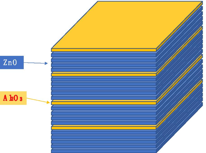
ZnO 및 Al2의 개략도 O3 성장 순서
작업 규칙의 더 복잡한 사용법은 다음과 같이 예제 2에 나와 있습니다.
$$\begin{정렬} &\left( {\begin{array}{*{20}c} {{\text{ZnO}}} \\ {{\text{Al}}_{2} {\text {O}}_{3} } \\ \end{array} } \right) =\left( {\begin{array}{*{20}c} {4.71} \\ 1 \\ \end{array} } \right) =\left( {\begin{array}{*{20}c} {4 + 0.71} \\ 1 \\ \end{array} } \right) \\ &\frac{2}{3 } =0.666 <0.71 <\frac{3}{4} =0.75 \\ &\left( {\begin{array}{*{20}c} E \\ F \\ \end{array} } \right) \left[ {\left( {\begin{array}{*{20}c} {4 + \frac{2}{3}} \\ 1 \\ \end{array} } \right)\left( { \begin{array}{*{20}c} {4 + \frac{3}{4}} \\ 1 \\ \end{array} } \right)} \right] \\ &\quad =E\ left( {\begin{array}{*{20}c} {4 + \frac{2}{3}} \\ 1 \\ \end{array} } \right) + F\left( {\begin{ array}{*{20}c} {4 + \frac{3}{4}} \\ 1 \\ \end{array} } \right) =\left( {\begin{array}{*{20} c} {4E + 4F + \frac{2}{3}E + \frac{3}{4}F} \\ {E + F} \\ \end{array} } \right) \\ &\quad =E + F\left( {\begin{array}{*{20}c} {4 + \frac{{\frac{2}{3}E + \frac{3}{4}F}}{E + F}} \\ 1 \\ \end{배열} } \right) \propto \left( {\begin{배열}{* {20}c} {4 + \frac{{\frac{2}{3}E + \frac{3}{4}F}}{E + F}} \\ 1 \\ \end{배열} } \right) =\left( {\begin{array}{*{20}c} {4.71} \\ 1 \\ \end{array} } \right) \\ &\frac{{\frac{2}{ 3}E + \frac{3}{4}F}}{E + F} =0.71 \Rightarrow {\text{E}} =12,{\text{F}} =13 \\ &\left( { \begin{array}{*{20}c} E \\ F \\ \end{array} } \right) =\left( {\begin{array}{*{20}c} {12} \\ { 13} \\ \end{배열} } \right) =12\left( {\begin{배열}{*{20}c} 1 \\ {1\frac{1}{12}} \\ \end{ 배열} } \right) =\left( {\begin{array}{*{20}c} {11} \\ 1 \\ \end{array} } \right)\left[ {\left( {\begin {배열}{*{20}c} 1 \\ 1 \\ \end{배열} } \right)\left( {\begin{배열}{*{20}c} 1 \\ 2 \\ \end{ 배열} } \right)} \right] \\ &\left( {\begin{array}{*{20}c} E \\ F \\ \end{array} } \right)\left[ {\left ( {\begin{array}{*{20}c} {4 + \frac{2}{3}} \\ 1 \\ \end{array} } \right),\left( {\begin{array} {*{20}c} {4 + \frac{3}{4}} \\ 1 \\ \end{array} } \right)} \right] \\ &\quad =\left( {\begin{ array}{*{20}c} E \\ F \\ \end{배열} } \right)\left[ { \left( {\begin{array}{*{20}c} 1 \\ 2 \\ \end{array} } \right)\left[ {\left( {\begin{array}{*{20}c } 4 \\ 1 \\ \end{배열} } \right)\left( {\begin{array}{*{20}c} 5 \\ 1 \\ \end{배열} } \right)} \right ],\left( {\begin{array}{*{20}c} 1 \\ 3 \\ \end{array} } \right)\left[ {\left( {\begin{array}{*{20 }c} 4 \\ 1 \\ \end{배열} } \right)\left( {\begin{배열}{*{20}c} 5 \\ 1 \\ \end{배열} } \right)} \right]} \right] \\ &\left( {\begin{array}{*{20}c} {4.71} \\ 1 \\ \end{array} } \right) \propto \left( {\ 시작{배열}{*{20}c} {12} \\ {13} \\ \end{배열} } \right)\left[ {\left( {\begin{array}{*{20}c} 1 \\ 2 \\ \end{배열} } \right)\left( {\begin{array}{*{20}c} 1 \\ 3 \\ \end{배열} } \right)} \right] \left[ {\left( {\begin{array}{*{20}c} 4 \\ 1 \\ \end{array} } \right)\left( {\begin{array}{*{20}c } 5 \\ 1 \\ \end{배열} } \right)} \right] =\left( {\begin{배열}{*{20}c} {11} \\ 1 \\ \end{배열} } \right)\left[ {\left( {\begin{array}{*{20}c} 1 \\ 1 \\ \end{array} } \right)\left( {\begin{array}{* {20}ㄷ } 1 \\ 2 \\ \end{배열} } \right)} \right]\left[ {\left( {\begin{array}{*{20}c} 1 \\ 2 \\ \end{배열 } } \right)\left( {\begin{array}{*{20}c} 1 \\ 3 \\ \end{array} } \right)} \right]\left[ {\left( {\begin {배열}{*{20}c} 4 \\ 1 \\ \end{배열} } \right)\left( {\begin{배열}{*{20}c} 5 \\ 1 \\ \end{ 배열} } \right)} \right] \\ \end{정렬}$$계획 1 :\(\left( {\begin{array}{*{20}c} {4.71} \\ 1 \\ \end{array} } \right) \propto 12\left[ {\left( {\begin{ array}{*{20}c} 4 \\ 1 \\ \end{array} } \right) + 2\left( {\begin{array}{*{20}c} 5 \\ 1 \\ \end {배열} } \right)} \right] + 13\left[ {\left( {\begin{array}{*{20}c} 4 \\ 1 \\ \end{배열} } \right) + 3 \left( {\begin{array}{*{20}c} 5 \\ 1 \\ \end{array} } \right)} \right]\).
플랜 2 \(\left( {\begin{array}{*{20}c} {4.71} \\ 1 \\ \end{array} } \right) \propto 11\left[ {\left[ {\left( { \begin{array}{*{20}c} 4 \\ 1 \\ \end{array} } \right) + 2\left( {\begin{array}{*{20}c} 5 \\ 1 \ \ \end{array} } \right)} \right] + \left[ {\left( {\begin{array}{*{20}c} 4 \\ 1 \\ \end{array} } \right) + 3\left( {\begin{array}{*{20}c} 5 \\ 1 \\ \end{array} } \right)} \right]} \right] + \left[ {\left[ { \left( {\begin{array}{*{20}c} 4 \\ 1 \\ \end{array} } \right) + 2\left( {\begin{array}{*{20}c} 5 \\ 1 \\ \end{배열} } \right)} \right] + 2\left[ {\left( {\begin{array}{*{20}c} 4 \\ 1 \\ \end{배열 } } \right) + 3\left( {\begin{array}{*{20}c} 5 \\ 1 \\ \end{array} } \right)} \right]} \right]\).
예제 2에서 계획 1의 작업은 다음과 같이 해석될 수 있습니다.
도식 1 ALD는 4배 ZnO 원자층 성장 과정과 한 번의 \({\text{Al}}_{2} {\text{O}}_{3}\) 원자층 성장 과정을 성장시킵니다. ALD는 ZnO 원자층 성장 과정 5회와 \({\text{Al}}_{2} {\text{O}}_{3}\) 원자층 성장 과정을 5번 반복하고 두 번 반복합니다.
도식 2 ALD는 4배 ZnO 원자층 성장 과정과 한 번의 \({\text{Al}}_{2} {\text{O}}_{3}\) 원자층 성장 과정을 성장시킵니다. ALD는 ZnO 원자층 성장 과정을 5번, \({\text{Al}}_{2} {\text{O}}_{3}\) 원자층 성장 과정을 3번 반복합니다.
방식 1을 12회, 방식 2를 13회 반복합니다.
플랜 2의 작업 해석은 플랜 1과 동일합니다.
그림 5a와 같이 원자층 증착 기술을 사용하여 AZO 전도층과 \({\text{Al}}_{2} {\text{O}}_{3}\) 발광층을 성장시킵니다. 2차원 기공 어레이의 마이크로채널 벽. 그런 다음 열 증착 기술을 사용하여 MCP의 양면에 Ni-Cr 전극층을 성장시키고[2, 4] MCP의 양면에 전극 링을 배치합니다. 위의 사항을 대비하여 ALD-MCP 저항성을 직접 테스트합니다. 이 조건에서 해당 MCP 저항을 MCP의 작동하지 않는 저항으로 정의합니다. Keithley 모델 6517B 전위계를 사용하여 10 −3 에서 MCP의 비작동 저항을 측정합니다. –10 −5 Pa 진공 [1, 4, 13].
<그림>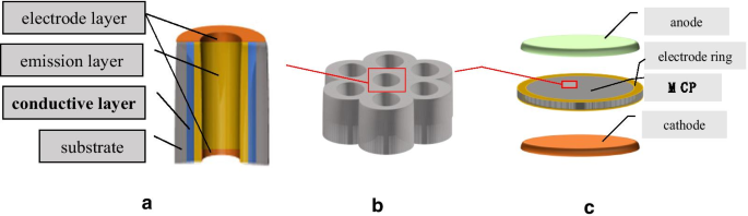
ALD-MCP 저항 테스트 개략도
그림 5c와 같이 전자총을 음극으로 사용하고 형광체 스크린을 양극으로 사용합니다. 전자총은 MCP에 입사 전자를 제공하고 형광체 스크린은 MCP에서 출력된 전자를 수신합니다. 또한 MCP가 작동 중일 때 고전압 형광체 스크린은 MCP의 균일성을 감지하기 위해 녹색 빛을 방출합니다[1, 21].
그림 1과 같이 전류를 측정하기 위해 MCP의 입력으로 100pA를 제공하는 전자총을 사용합니다. 2차 전자의 수가 증가함에 따라 발광층이 많은 양의 전하를 잃고 전도층이 발광층에 전하의 흐름을 연속적으로 제공하는 조건이 있을 것이다. 이 조건에서 해당 MCP 저항을 MCP의 작동 저항으로 정의합니다. 작동 저항의 진공 환경은 10 −3 입니다. –10 −5 파.
AZO-ALD-MCP 샘플의 단면 SEM 사진은 그림 6에 나와 있습니다. 우리는 표 1에 표시된 일련의 AZO 전도층과 그림 7에 해당 작동 및 비 작동 저항을 설계했습니다. 같은 그림에서 우리는 또한 기존 MCP의 작동 및 비 작동 저항을 보여줍니다. AZO-ALD-MCP의 비 작동 저항과 비교하여 AZO-ALD-MCP의 작동 저항은 크게 감소합니다. 그러나 기존 MCP의 작동 저항과 비 작동 저항 사이에는 큰 차이가 없습니다. 전압이 증가함에 따라 AZO-ALD-MCP의 작동 저항은 기존 MCP보다 현저히 낮아집니다. 동일한 전압 조건에서 AZO-ALD-MCP의 작동 및 비 작동 저항은 안정적입니다. 앞서 언급한 특성에는 크게 두 가지 이유가 있다고 생각합니다.
<그림>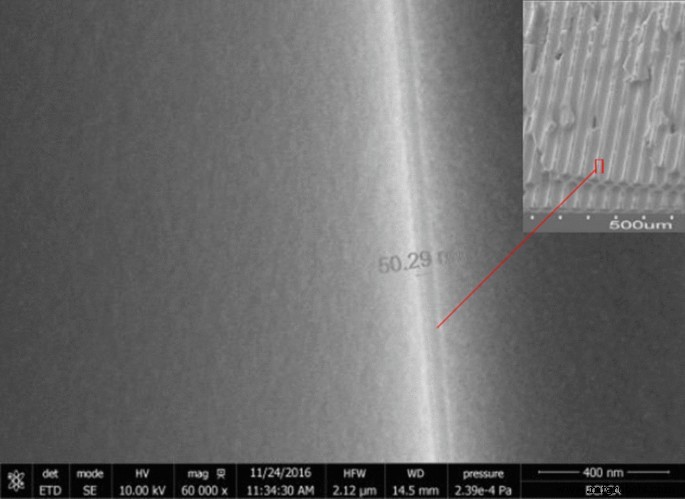
AZO-ALD-MCP의 단면 SEM 사진
<그림>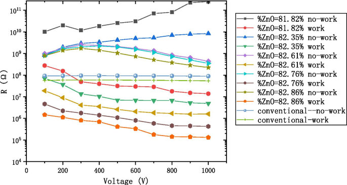
다른 비율의 AZO-ALD-MCP와 기존 MCP의 전압 다이어그램을 사용한 작동 저항 및 비 작동 저항
공식 [21]에 따르면,
$$R_{{{\text{MCP}}}} =R_{0} \exp \left[ { - \beta_{T} \left( {T_{{{\text{MCP}}}} - T_{ 0} } \오른쪽)} \오른쪽]$$AZO는 납유리에 비해 NTC(음의 온도 계수)가 높은 재료이므로 동일한 온도와 초기 저항에서 저항이 낮아집니다. 게인을 생성하는 과정에서 AZO는 고전압에서 입사 전자에 의해 충격을 받아 더 많은 전자-정공 쌍을 생성하여 전류를 증가시킵니다.
재료 저항의 안정성을 설명하기 위해 작동 저항에 대한 비 작동 저항의 비율을 정의합니다.
$$\카파_{R} =\frac{{R_{n} }}{{R_{w} }}$$그림 8은 AZO-ALD-MCP의 \(\kappa_{R}\)가 약 10 2 임을 보여줍니다. –10 3 배이며, 기존 MCP의 \(\kappa_{R}\)는 약 2-3배입니다. 이것은 AZO-ALD-MCP의 저항 변화가 더 분명하다는 것을 보여줍니다. 따라서 MCP 저항에 대한 정의로 작동하지 않는 저항이라는 기존 개념을 작동 저항으로 대체해야 합니다.
<그림>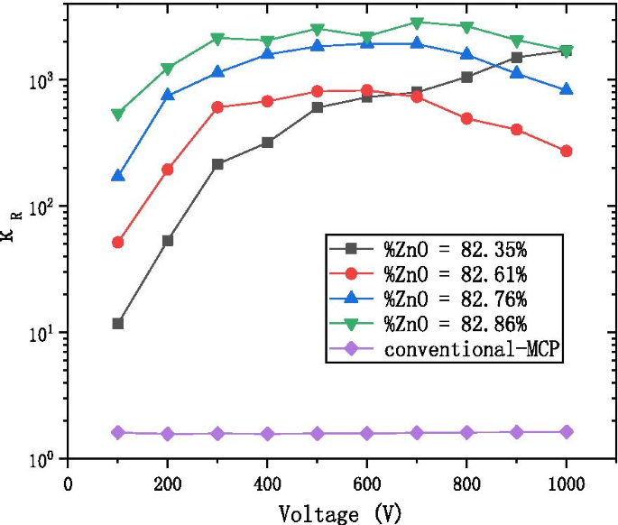
케이 R AZO-ALD-MCP의 다른 비율에서 전압 다이어그램으로
그림 9는 작동 전압에 대한 '인접한' 재료 설계의 저항 비율 \(L_{R}\)을 보여줍니다. 비율 \(L_{R}\)은 다음과 같이 정의됩니다.
$$L_{R} =\frac{{R\left( {4 + \frac{N - 1}{N}} \right)}}{{R\left( {4 + \frac{N}{N + 1}} \right)}}$$ <그림>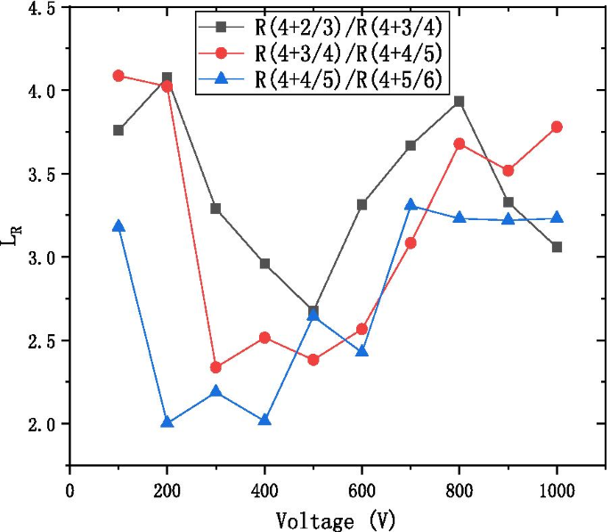
The resistance of the step length LR with the voltage diagram at the different ratio of the working resistance of neighbor formula
where
$$\left( {\begin{array}{*{20}c} {{\text{ZnO}}} \\ {{\text{Al}}_{2} {\text{O}}_{3} } \\ \end{array} } \right) =\left( {\begin{array}{*{20}c} {4 + \frac{N - 1}{N}} \\ 1 \\ \end{array} } \right) =\left( {\begin{array}{*{20}c} 1 \\ {N - 1} \\ \end{array} } \right)\left[ {\left( {\begin{array}{*{20}c} 4 \\ 1 \\ \end{array} } \right)\left( {\begin{array}{*{20}c} 5 \\ 1 \\ \end{array} } \right)} \right]$$그리고
$$\left( {\begin{array}{*{20}c} {{\text{ZnO}}} \\ {{\text{Al}}_{2} {\text{O}}_{3} } \\ \end{array} } \right) =\left( {\begin{array}{*{20}c} {4 + \frac{N}{N + 1}} \\ 1 \\ \end{array} } \right) =\left( {\begin{array}{*{20}c} 1 \\ N \\ \end{array} } \right)\left[ {\left( {\begin{array}{*{20}c} 4 \\ 1 \\ \end{array} } \right)\left( {\begin{array}{*{20}c} 5 \\ 1 \\ \end{array} } \right)} \right]$$As can be observed from Fig. 9, the LR value ranges from 2 to 4.5 to adjust ratio of conductive material ZnO and high resistance material \({\text{Al}}_{2} {\text{O}}_{3}\). And it proves the feasibility of WYM operation to design laminated materials.
Figure 10 shows the working resistance with respect to the percentage of ZnO cycles (%ZnO), where %ZnO is defined to be:
$${\text{\% ZnO}} =\frac{{{\text{ZnO}}}}{{{\text{ZnO}} + {\text{Al}}_{2} {\text{O}}_{3} }}{*}100\left( {\text{\% }} \right)$$
The working resistance with the percentage of ZnO cycles diagram at the different voltage
under various voltage conditions, ranging from 100 to 1000 V. It decreases that the working resistance under the same voltage with the increase in the percentage of ZnO cycles. It can be the same that the working resistance under different the percentage of ZnO cycles and under the different condition of voltage. Therefore, the AZO-ALD-MCP of different formulations works under its specific voltage to meet the MCP resistance index.
We define the ratio of the resistance difference under the different condition of voltage and the voltage difference to describe the effect of the voltage on the resistance of MCP:
$$r =\left| {\frac{{R_{U} - R_{V} }}{U - V}} \right| =\left| {\frac{{R_{1000v} - R_{100v} }}{1000 - 100}} \right|$$Figure 11 shows that the effect of the voltage on the resistance of AZO-ALD-MCP decreased and gradually stabilized with the increase in the percentage of ZnO cycles. Therefore, the preparation of AZO-ALD-MCP should try to choose a formula with a large percentage of ZnO cycles.

The r with the percentage of ZnO cycles diagram at the working state
Based on the above analysis, we have put forward the reference to the working resistance for the conductive layer of ALD-MCP. As shown in Fig. 5a, we design the AZO conductive layer of AZO-MCP by using the WYM operation and temperature adjustment based on the working resistance. We use atomic layer deposition technology to grow the \({\text{Al}}_{2} {\text{O}}_{3}\) emission layer on microchannel wall of the two-dimensional pore arrays [3, 11, 22]. In Fig. 12a, the gain from our AZO-ALD-MCP is compared to that of a conventional MCP under different voltages. As can be observed, our preparation method of the AZO-ALD-MCP provides a larger gain than that of a conventional MCP. Figure 12b shows the phosphor screen with uniform green light under high pressure, thus proving the uniformity of the material deposited on the wall of each microchannel and the uniformity of the AZO-ALD-MCP field of view.

The gain with the voltage diagram at the AZO-ALD-MCP and conventional-MCP
We defined the working and non-working resistance of the microchannel plate. Aiming at the required resistivity of the microchannel plate in the region with extremely narrow zinc content requirement (70–73%), an algorithm for growing the AZO conductive layer is proposed. Compared with the conventional MCP, we found a large difference between the working and non-working resistance and there is also a huge difference under different voltages. Therefore, we analyze the data by defining \(\kappa_{R} ,L_{R} ,\% {\text{ZnO}},r\). MCP should try to choose a formula with a large percentage of ZnO cycles. We recommend using the working resistance as an ALD-MCP resistance indicator in industrial production. Building on our results as described in this work, our studies will help to find even better materials as the conductive layer for the ALD-MCP.
나노물질
로봇은 다양한 목적을 위해 설계되었습니다. 로봇이 사용되는 특정 목적에 따라 적절한 기능을 위해서는 고유한 디자인이 필수적입니다. 로봇 설계 프로세스는 로봇이 사용될 문제 또는 작업을 정의하는 것으로 시작됩니다. 설계를 생성하기 전에 특정 요구 사항과 구성 목적을 해결해야 합니다. 다음으로, 로봇이 어떻게 움직이고, 물체를 조작하고, 감지하고, 지능을 얻는지와 같은 작업 및 실제 기능의 세부 사항을 식별하기 위한 연구가 진행됩니다. 이 시점에서 프로토타입을 생성하여 설계를 테스트하고 문제를 해결할 수 있습니다. 그런 다음 로봇 구
FDM 3D 프린터의 기능적 부분에 대해 이야기할 때 레이어 팬은 가장 중요한 구성 요소 중 하나입니다 찾을 수 있습니다. 3D 프린터에는 일반적으로 HotEnd 영역에 두 개의 팬이 있습니다. 하나는 HotEnd 디퓨저 냉각을 담당하고 다른 하나는 노즐에서 나오는 재료를 냉각합니다. 이 기사에서는 후자인 레이어 팬에 대해 이야기하겠습니다. 필요한 경우 모든 사용자는 노즐이 동일한 영역에서 지속적으로 움직이는 작은 영역 영역으로 일부 부품을 인쇄하려고 시도했으며, 이는 부품을 연화시키는 과도한 온도를 유발하는 프로세스입니다. 같