

나노물질

산업 제조
대표적인 와이드 밴드갭 반도체 재료로서 질화갈륨(GaN)은 우수한 재료 특성(예:높은 전자 이동도, 높은 전자 포화 속도 및 임계 전기장)으로 인해 점점 더 많은 관심을 받고 있습니다. 수직 GaN 장치가 조사되었으며 전력 전자 응용 분야에서 가장 유망한 후보 중 하나로 간주되며 고전압, 고전류 및 높은 항복 전압에 대한 용량이 특징입니다. 그 중 수직 GaN 기반 PN 접합 다이오드(PND)는 높은 에피택시 품질과 소자 구조 설계를 기반으로 상당한 성능 향상을 보여주고 있습니다. 그러나 장치 에피택시 품질은 추가 개선이 필요합니다. 소자의 전기적 성능 측면에서 소자 에지에서의 전기장 밀집 효과는 조기 고장을 초래하고 GaN 재료의 방출 우수성을 제한하는 긴급한 문제이지만 현재는 에지 종단에 의해 완화됩니다. 이 검토에서는 재료 에피택시 성장 및 에지 터미널 기술의 발전을 강조하고 재료 및 장치에 대한 현재 GaN 개발 및 실리콘 탄소(SiC)에 대한 잠재적 이점, GaN 쇼트키 장벽 다이오드(SBD)와 PND 간의 차이점을 다음과 같이 탐색합니다. 메커니즘과 기능, 측면 장치에 비해 수직 장치의 장점에 대해 설명합니다. 그런 다음 검토에서는 초기 수직 GaN PND를 포함하여 전력 시스템에 사용되는 수직 GaN PND의 전망과 설계 추세를 보여줍니다.
세계 에너지 소비는 산업과 경제의 급속한 성장으로 인해 지난 수십 년보다 훨씬 더 빠르게 증가하고 있습니다. 따라서 에너지 소비 증가 문제를 완화하기 위해서는 고도의 에너지 절약 기술이 필요합니다.
실리콘 기반 장치는 현재 전력 장치 중 지배적인 유형입니다[1]. 이들 전력소자 중 IGBT(Insulated Gate Bipolar Transistor) 구조가 중요한 역할을 하며, 발명 이후 전력 바이폴라 접합 트랜지스터(BJT) 및 금속 산화물 반도체 전계 효과 트랜지스터(MOSFET)를 대체하는 추세를 보이고 있습니다. 1982년 IGBT[2]. 현재 IGBT는 변환 및 전송을 위한 전력 전자 분야의 필수 요소입니다[3]. 그러나 실리콘 기반 전력 장치는 현재까지 기본적인 재료 한계에 도달했으며 전기 에너지 응용 분야에서 널리 활용되고 있습니다.
뛰어난 특성을 감안할 때 GaN은 와이드 밴드갭 반도체 재료 중 하나입니다(SiC, GaN, Ga2 O3 및 다이아몬드) Si 기반 장치에 대해 지정된 항복 전압에 대해 낮은 커패시턴스와 저항을 갖는 전력 장치를 제조할 수 있습니다. 따라서 전력 전자 시스템을 위한 낮은 에너지 소비, 높은 전력 밀도 및 높은 변환 효율을 갖는 GaN 기반 장치가 기대됩니다.
표 1에서 볼 수 있듯이 GaN은 더 높은 전자 포화 속도와 더 높은 임계 전기장에 기인하는 특성인 SiC(상업화됨)보다 훨씬 더 높은 BFOM(Baliga's Figure of Merit)을 가지고 있습니다. 그러나 SiC는 열전도율이 더 좋습니다. 또한 GaN은 더 높은 캐리어 이동도 µ를 가지고 있습니다. 더 높은 열전도율과 p - 및 n -Ga2에 비해 유형 도핑 O3 . 한편, 궁극적인 와이드 밴드갭 반도체인 다이아몬드는 실용화 단계에 이르기까지 상당한 진전이 있어야 한다. 지금까지 3단자 소자(HFET(Heterostructure Field-Effect Transistor) 및 MOSFET)와 2단자 소자(SBD 및 PND)와 같은 GaN 기반 소자가 주요 연구 주제가 되었으며 그 분야에서 큰 진전을 이룩했습니다. 전력 정류 및 전력 변환의 애플리케이션.
고유한 재료 특성에서 GaN은 더 넓은 에너지 밴드갭, 더 높은 임계 전기장, 더 높은 전자 포화 속도 및 전력 장치에 대해 3-4배 더 나은 BFOM을 포함하여 SiC보다 약간 우수한 이점을 가지고 있습니다[6]. 따라서 뛰어난 기능을 고려할 때 GaN 기반 장치는 SiC 기반 장치를 능가해야 합니다. 실제 적용에서 수직 GaN 기반 장치는 우수한 재료 특성으로 인해 고전력 밀도와 높은 작동 주파수(그림 1)에 필수적입니다.
<그림>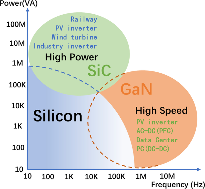
GaN 및 SiC 전력 스위칭 트랜지스터의 잠재적 응용 [7]
가장 성숙한 와이드 갭 반도체인 SiC 장치는 지난 10년 동안 눈부신 발전을 이루었으며 고전압, 낮은 특정 온 저항 및 빠른 스위칭 속도 측면에서 유망한 성능을 보여줍니다[8]. 1980년 이후의 심오한 연구 기반과 낮은 결함(<10 4 cm −2 ), SiC SBD 및 접합 전계 효과 트랜지스터(JFET)는 2001년 이후 최초로 상용화된 SiC 기반 장치였습니다. MOSFET 및 BJT를 포함한 기타 SiC 기반 전력 장치는 고전압 및 전력 응용 분야에서 성공적으로 개발되었으며 인상적인 성능을 보여주었습니다. 성능 [9].
SiC와 비교하여 GaN 장치는 매우 느리게 개발되었습니다. 그들의 불만족스러운 재료 품질은 이론적으로 우수한 특성의 일부 실현을 방해합니다. GaN 기판의 부족을 감안할 때 GaN 장치에 대한 대부분의 연구는 주로 이 단계에서 측면 구조(예:AlGaN/GaN 이종 구조)를 기반으로 합니다. 2000cm 2 의 더 높은 전자 이동도 /V s(AlGaN/GaN의 2차원 전자 가스(2DEG)), 1000cm 2 /V s(대량 GaN) 및 2.5 × 10 7 의 더 높은 포화 속도 SiC에 비해 cm/s인 AlGaN/GaN 장치는 고주파 응용 분야에 선호되며 SiC 장치에 비해 전력 와트가 낮습니다[10]. 고주파장에서 AlGaN/GaN SBD는 우수한 전기 전송 성능을 달성하고 와트 수준에서 마이크로파 및 밀리미터파 응용 분야에 더 적합합니다[11, 12]. AlGaN/GaN SBD는 GaN SBD의 대표적인 소자이다. 2DEG의 높은 이동성은 AlGaN/GaN SBD가 수직 SBD에 비해 고주파 애플리케이션에서 엄청난 성능 이점을 보여주고 낮은 턴온 전압도 유지한다는 것을 의미합니다. 최근 AlGaN/GaN SBD는 6.4W의 입력 전력과 0.38V의 턴온 전압과 항복 전압(BV ) 3000V [13, 14]. 최대 차단 주파수는 70nm의 양극-음극 거리에서 0V에서 1THz에 가깝습니다[15].
GaN 기반 전력 장치의 경우 GaN 기판(벌크 GaN)은 불일치를 제거하기 위해 호모 에피택시 기술을 사용할 수 있는 에피택시 성장에 이상적입니다. 높은 전위 밀도가 BV와 같은 성능 특성에 영향을 줄 수 있기 때문에 벌크 GaN의 낮은 전위 밀도는 에피택셜 기판에 필수적입니다. , 역 누설 전류, 생산량 및 신뢰성 [16]. 수직 GaN 기반 장치의 개발은 최근 몇 년 동안 GaN 기판의 발전에 의해 주도되었습니다. 그러나 수직 3극관에 대한 상대적으로 미숙한 기술을 고려할 때 수직 GaN 다이오드는 이 초기 단계에서 뜨거운 연구 주제가 되었습니다. AlGaN/GaN SBD와 비교하여 수직 GaN SBD는 낮은 역 회복 시간 및 낮은 전도 손실과 같은 높은 스위칭 속도와 같은 주파수 필드에서 유사한 이점을 가지고 있습니다. 그럼에도 불구하고 후자는 전자보다 전류 밀도가 크고 누설 경로가 적습니다[17, 18].
GaN 기판에 대해 몇 가지 문제가 발생했습니다. 첫째, GaN 기판은 현재 10 4 전위 밀도로 사용할 수 있습니다. –10 6 cm −2 그러나 이러한 전위 밀도는 여전히 Si 및 SiC 기판의 전위 밀도보다 훨씬 높습니다[19]. 둘째, 4~6인치 웨이퍼 크기와 합리적인 비용(10유로/cm 2 ) SiC, 2~3인치 크기 및 상대적으로 높은 비용(100유로/cm 2 ) GaN 기판의 GaN 상용화와 대규모 생산성을 저해한다[20]. 공급 업체를 늘리는 것 외에도 외부 기판(Si, 사파이어 또는 SiC)에 대한 이종 에피택시는 GaN 기판 비용을 줄이는 대체 방법이지만 상대적으로 높은 불일치 및 결함 문제를 해결해야 합니다.
벌크 재료에서 앞서 언급한 문제 외에도 GaN 다이오드의 과제는 p의 고품질을 달성하는 것입니다. - 유형 재료. p를 형성하는 비교적 진보된 기술과 관련하여 - Al 이온 주입에 의한 유형 SiC, 미성숙 p -타입 이온 주입 기술 및 p에 대한 낮은 수용체 활성화 -형 GaN은 GaN 기반 장치의 구조 및 제조 개발을 제한하는 중요한 장애물입니다. 따라서 GaN 다이오드 성능을 개선하고 이 리뷰의 핵심 부분을 구성하기 위해 다양한 종류의 에지 종단 구조가 제안됩니다.
10년 전까지 SBD 및 PND를 포함한 대부분의 GaN 다이오드는 벌크 GaN 기판을 사용할 수 없기 때문에 측면 또는 준수직 소자 구조를 형성하는 외부 기판에 제조되었습니다. 횡형 또는 준수직형 다이오드는 우수한 전기적 특성을 나타내지만 여전히 소자 구조의 고유한 단점이 있습니다[21]. 첫째, 불일치와 결함이 불가피하다. 그런 다음 외부 기판 위의 GaN 장치의 경우 GaN 드리프트 층과 외부 기판 사이에 버퍼가 필수적입니다. 따라서 버퍼 층의 응력 완화는 웨이퍼 휘어짐을 유발하여 GaN 에피택시 층의 두께를 낮출 것입니다[22]. 또한, 큰 열 경계 저항(기판을 포함하는 GaN)은 높은 전력 밀도에서 작동하는 GaN 장치의 장치 성능에 심각한 영향을 미칩니다[23].
에피택시 기술의 발전에 따라 수직 GaN 장치에 채택된 낮은 전위 밀도를 가진 독립형 GaN(FS-GaN) 기판이 크게 발전했습니다. FS-GaN 기판의 호모에피택셜 GaN 재료 품질은 분명히 개선되었으며 전력 응용 분야에 대한 잠재력을 보여줍니다. 수직 GaN 장치는 측면 GaN 대응물의 단점을 완화할 수 있습니다. 첫째, 더 두꺼운 GaN 에피택셜 레이어는 버퍼 없이 성장할 수 있으며 더 높은 BV (측면 GaN 디바이스의 것을 초과함)은 드리프트 층의 두께에 의해 얻어지고 결정될 수 있다. 한편, 최대 전기장은 소자 내부에 위치하며 소자 표면에서 멀리 떨어져 있다(측면 소자에서 일반적으로 발생하는 전자 트래핑 효과 제거). FS-GaN 기판의 고품질을 감안할 때 수직 GaN 장치는 2011년부터 연구되었습니다[24]. 그 이후로 BV가 높은 수직 GaN PND 낮은 온 상태 저항이 제작되어 놀라운 성능을 달성했습니다.
실제 적용을 위해 다이오드는 전력 변환 및 반전을 위한 필수 구성 요소입니다[25]. GaN의 고유한 재료 특성으로 인해 GaN 기반 다이오드(SBD 및 PND)는 전력 애플리케이션의 요구 사항을 충족할 것으로 예상되는 주목할만한 성능을 나타냅니다. 그림 2에서 볼 수 있듯이 PND는 다양한 구조와 600~5000V의 내전압을 가진 GaN 장치 중 가장 넓은 범위를 가지며 이는 더 넓은 응용 시나리오를 나타내는 기능입니다.
<사진>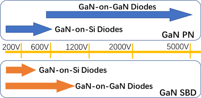
최근 몇 년 동안 보고된 주요 수직 GaN 전력 장치의 장치 유형, 보고서 및 전압 등급 개요[26]
소수 캐리어 저장 문제가 없고 SBD 장벽 높이가 낮은 PND와 비교하여 GaN SBD는 낮은 순방향 턴온 전압(V 켜기 ) 및 빠른 역회복, 그리고 이러한 특성은 SBD의 장점이 낮은 전도/스위칭 손실, 고주파수 동작에서 드러나지만 BV가 낮다는 것을 나타낸다. PND보다 값; 또한 높은 턴온 전압은 높은 전도 손실을 초래하고 회로 및 시스템의 효율성을 저하시킬 수 있습니다[27, 28].
고전력 필드에서 준 수직 또는 수직 SBD는 AlGaN/GaN SBD에 비해 탁월한 이점을 가지고 있습니다[29]. 또한 낮은 턴온 전압(<0.5V)은 낮은 일함수 금속으로 장벽 높이를 조정하여 달성됩니다. 그러나 낮은 배리어 높이는 쉽게 높은 역 누설 전류를 발생시키고 BV를 낮출 수 있습니다. . 따라서 성능 향상을 위해 다양한 에지 종단 구조가 제안됩니다. 다양한 에지 종단 기술[27, 28, 30, 31]의 지원을 통해 KA/cm 2 의 높은 전류 밀도 BV 등급 s 1kV 초과가 확인되었습니다. 한편, 수직형 SBD는 177~183GHz와 같은 고주파수 및 0V에서 최대 902GHz 차단 주파수와 같은 뛰어난 성능을 보여주며, 이는 테라헤르츠 무선 통신 시스템의 전원에 기대되는 기능입니다[12, 32].
n에 대해 -유형 GaN, p 금속 유기 화학 기상 증착(MOCVD) 및 분자 빔 에피택시(MBE)에 의해 성장된 -형 GaN은 Mg를 수용체로 사용하여 도입되었습니다[33]. GaN SBD와 비교할 때 GaN PND는 낮은 비저항(R 켜기 A ) 및 적절한 장치 안정성 및 서지 전류 억제 기능. 높은 턴온 전압(> 3 V)과 상대적으로 낮은 스위칭 속도에도 불구하고 높은 장벽 높이와 높은 BV로 인해 누설 전류가 매우 낮습니다. 얻어진다. 높은 BV 0.6~5kV는 GaN 기반 PND에서 가장 뛰어난 성능입니다. 따라서 GaN 기반 PND는 고효율 및 낮은 에너지 손실이 요구되는 고전력 애플리케이션을 위한 차세대 전력 시스템의 중요한 빌딩 블록으로 큰 잠재력을 가지고 있습니다[34]. 수직 GaN SBD와 유사하게 GaN PND의 에지 종단도 양극 주변의 전기장 밀집 현상을 완화하기 위해 제작되며, 이 기능은 이 기사 뒷부분에서 자세히 설명합니다.
파워 디바이스에서 PN 접합은 새로운 접합 구조로 취급될 수도 있습니다. 높은 BV 활용 PND의 낮은 역 누설 전류, 높은 스위칭 성능 및 SBD의 낮은 턴온 전압을 동시에 사용하는 JBS(접합 장벽 쇼트키) 및 병합된 PN 쇼트키(MPS)를 포함한 새로운 장치 구조는 다음을 통해 SBD와 PND의 조합을 생성합니다. p의 형성 -쇼트키 접촉 영역의 그리드 영역 유형. JBS 또는 MPS 장치는 SBD의 순방향 전도와 PND의 역차단 특성을 가지고 있으며 기존 PND 및 SBD보다 각각 더 나은 스위칭 성능과 더 높은 역전압을 가질 것으로 기대됩니다[35].
고출력 애플리케이션 외에도 GaN PND는 GaN 기반 PN 접합 포토다이오드에서 수 pA의 낮은 암전류 때문에 발광 다이오드(LED), 광검출기 및 화염 감지와 같은 광전자 장치에도 채택됩니다. , 37].
GaN의 우수한 재료 특성을 기반으로 GaN 기반 장치가 널리 연구되어 왔으며 가장 뜨거운 반도체 재료 중 하나로 전력 전자 응용 분야에 활용되었습니다. GaN 기반 소자 중에서 수직 GaN 기반 PND가 상당히 연구되어 왔으며 우수한 BFOM을 보여줍니다. 에지 단자 기술은 양극 패드 주변에 밀집된 전기장을 완화하는 데도 필수적입니다.
이 리뷰에서는 주요 강조점인 재료 에피택시 성장 및 에지 터미널 기술의 발전에 이어 현재 GaN 개발, 메커니즘 및 기능 측면에서 GaN SBD와 PND의 차이점, 측면 디바이스에 비해 수직 디바이스의 장점을 설명합니다. . 이 검토는 초기 수직 GaN PND를 포함하여 전력 시스템에 사용되는 수직 GaN PND의 전망을 제공하고 설계 추세를 보여줍니다. 수직 GaN PND의 다른 층에 해당하는 에피택셜 성장의 개발은 섹션에서 소개됩니다. 2. 에지 단말 기술은 Sect. 3. 섹션에서. 도 4에서, Si 기판 상의 수직 GaN PND가 대안적인 방법으로 설명된다. 마지막으로 수직 GaN PND의 향후 발전에 대한 결론과 전망이 제공됩니다.
주류 에피택시 공정으로서, 수직 디바이스 에피택셜 층은 현재 주로 수소화물 기상 에피택시(HVPE)에 의해 제조된 전도성 GaN 기판에서 MOCVD에 의해 성장됩니다. 이 구조에서 기판의 품질은 다음 에피택시 구조에 직접적인 영향을 미칩니다. 장치의 많은 고장 메커니즘은 기판 에피택시 품질에서 비롯됩니다[38]. 순방향 및 역방향 I를 더욱 향상시키려면 고품질의 전도성 GaN 기판을 얻어야 합니다. –V 성능, 특히 역 누설 전류 및 BV 능력.
HVPE에 의해 성장된 기판은 상대적으로 저렴한 비용과 재현성 때문에 대량 생산에 가장 편리한 방법으로 여겨져 왔다. 그러나 초기 단계에서 미성숙 성장 기술은 HVPE에 의해 성장된 GaN 기판이 높은 배경 캐리어 농도(> 10 19 cm −3 ) 및 불만족스러운 결정 품질. 따라서 HVPE는 소자 구조를 성장시키기 위해 채택되지 않았다[39]. 에피택시 성장 기술의 급속한 발전으로 HVPE에 의한 고품질 벌크 GaN 재료가 점차 가능해지고 있다[40, 41]. 기판 외에도 디바이스의 부분적 에피택셜 층은 이제 HVPE에 의해 성장될 수 있으며 HVPE와 MOCVD 에피택셜 프로세스를 탄소가 없는 기술과 결합하여 성장된 디바이스에 비해 더 높은 전류 균일성과 GaN 표면의 매크로스텝을 제거할 수 있습니다. MOCVD에 의해서만 [42].
현재 최소 전위 밀도가 10 4 미만인 상용 GaN 기판 cm −2 사용할 수 있습니다. 낮은 결함 밀도 GaN 기판의 GaN 수직 PND가 처리되었습니다. 그러나 웨이퍼 보잉은 여전히 문제입니다. 유망한 솔루션으로, 암모노열 방법은 더 나은 에피택시 품질을 가진 GaN 기판을 얻을 수 있습니다. 고압 오토클레이브와 초임계 암모니아를 사용하면 나사 전위를 10 4 까지 크게 줄일 수 있습니다. –10 5 cm −2 [43]. 암모니아 열법을 사용하여 0.001 Ω cm 2 의 낮은 저항 고도로 도핑된 n을 갖는 GaN 기판에서 -유형(1 × 10 19 –1 × 10 20 cm −3 ) 및 BV가 보고되었습니다. 3kV [44]. 그러나 암모노열법의 단점은 80~90μm/day 정도의 낮은 성장률로 실제 생산에 불리한 특성입니다. 성장률을 높이고 높은 재료 품질을 유지하는 것도 후속 연구를 위한 수익성 있는 방향입니다.
상용 GaN 기판 외에도 비-Ga 평면(c -평면) 기판. 일반적으로 Ga-polar(즉, c -평면) 기판은 GaN 수직 장치에 사용됩니다. 그러면 다음 에피택시 레이어는 급격한 편광 효과를 보입니다. 그러나, Ga-polar 대응물의 반대 방향에서, 호모에피택셜 층은 N -극성 방향은 더 높은 분해 온도와 극성 종속 특성으로 인해 고유한 장치 특성을 나타냅니다[45, 46]. N -극성 단결정 FS-GaN 기판, 가장자리 종단 없이 2.2MV/cm의 전기장 및 BV 달성 N2에서 2.4kV의 O 표면 플라즈마 처리 및 필드 플레이트(FP) [46, 47]. 또 다른 특수 GaN 기판으로 m -평면은 또한 m에서 Ga:N이 1:1인 비극성 특성을 감안할 때 폭넓은 관심을 받습니다. - c에서 Ga에 대한 평면 -극성 및 N만 N -극성 기질. 이 비극성 GaN 기판을 사용하여 FP 또는 에지 종단이 없는 2.0MV/cm의 임계 전기장 및 높은 온/오프 비율로 PND의 특성이 보고되었습니다[48].
고품질 전도성 GaN 기판이 존재하기 전에 GaN PND는 주로 Si, SiC 및 사파이어를 포함한 외부 기판에 제조되었습니다. 따라서 장치의 구조는 항상 측면 구조로 제한되었습니다. 에피택시 품질을 향상시키기 위해 측면 구조를 기반으로 하는 방법이 제안되었습니다. 측면 장치의 창 영역에 낮은 스레딩 전위(TD)가 주어지면 마스크를 가로질러 측면으로 성장한 GaN 에피택셜 층은 훨씬 더 낮은 TD 밀도를 달성할 수 있습니다. 따라서, 측면 PND용 사파이어 기판 상에 GaN 에피택셜 층을 성장시키기 위해 측면 에피택시 과성장이 수행되었다. 역 누설 전류는 100배 정도 억제되었습니다[49].
에피택시 기술의 발달로 3 × 10 –6 의 낮은 전위 밀도를 갖는 고품질 단결정 GaN 기판 cm −2 GaN PND가 GaN 기판에 제작되었습니다. MOCVD 성장에 의한 상부 에피택시 층과 결합하여 소자는 낮은 누설 전류와 높은 BV를 보여줍니다. 6~40μm의 드리프트 두께에 해당하는 600V~4kV[16, 50]. 사파이어 기판 상의 소자에 대하여 역 누설 전류 및 BV 크게 개선되었습니다[51].
기본 GaN 기판을 사용하면 일반적으로 외부 기판과 같은 PND 에피택시 구조에서 특별한 버퍼층이 발생하지 않습니다. PND의 버퍼층이 GaN 기판에 미치는 영향을 기준으로 조사했습니다. 버퍼층의 존재는 드리프트층의 결함 밀도가 낮다는 것을 의미한다. 한편, 더 높은 BV 더 얇은 드리프트 층으로 얻을 수 있지만 더 두꺼운 버퍼 층으로 얻을 수 있습니다. 장치의 역 누설 전류도 개선되었습니다. 이러한 장치 매개변수는 버퍼층의 두께와 강한 관계를 나타내므로 장치의 순방향 특성에 약간의 영향을 미칩니다[52].
상부 에피택시 층은 이 부분에서 논의된 바와 같이 MOCVD, 금속 유기 기상 에피택시(MOVPE) 및 MBE에 의해 증착됩니다. PND의 에피택셜 구조는 고도로 도핑된 n + -GaN 층 및 n의 드리프트 층 - -기판과 p 사이의 GaN -GaN(그림 3). 고도로 도핑된 n + -GaN 레이어는 일부 보고서에서 전도성 GaN 기판의 전이 레이어 역할을 합니다.
<그림>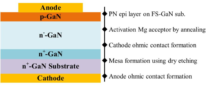
GaN 수직 PND의 개략 구조 및 제조 공정
일반적으로 BV 장치의 응용 시나리오를 결정합니다. 예를 들어, BV가 높을수록 GaN에 비해 SiC 장치의 경우 전기 자동차 및 총알 열차와 같은 고전력 및 고전압 응용 분야에서 SiC 장치를 활용할 수 있습니다(그림 1). 유사하게, PN 다이오드는 일반적으로 쇼트키 다이오드 및 HEMT와 관련하여 더 높은 전압에서 적용됩니다. PND에서 BV 주로 드리프트 레이어에 의해 수행됩니다(약하게 도핑된 n - -GaN 층) 공핍 영역의 확장(인가된 전압 V으로 식 1에 표시됨) V 장치가 역 바이어스 상태일 때 순방향/역방향 바이어스에 대해 양/음입니다. 또한 역 바이어스가 더 증가함에 따라 고장이 발생합니다.
$${W_{\text{D}}} =\sqrt {\frac{{2{\varepsilon_{\text{s}}}\left( {{V_{{\text{bi}}}} - V } \right)}}{q}\frac{{{N_{\text{A}}} + {N_{\text{D}}}}}{{{N_{\text{A}}}{N_ {\text{D}}}}}$$ (1)여기서 S , q , V 바이 , N D , 및 N A 접합 영역, 전자 전하, 내장 전위, 도너 농도 및 억셉터 농도는 각각 [53]입니다.
공핍 폭에 따라 장치는 비펀치 스루 [W D> 와 디엠 (와 디엠 :최대 공핍층 너비)] 및 펀치스루(W D <와 디엠 ). 에피택시 구조 및 에지 문제를 감안할 때 대부분의 GaN 수직 장치는 펀치 스루 유형에 해당합니다. 즉, 공핍 영역이 전체 n 이상으로 확장됩니다. − -GaN 층 및 도달 n + -파괴 전의 GaN 기판.
또한, Eq. (2), BV 두께를 늘리고 n - 드리프트 층의 유형 도핑 농도.
$${\text{BV}} ={E_{\text{C}}}t - \frac{{q{N_{\text{D}}}{t^2}}}{{2{\varepsilon_0 }{\varepsilon_{\text{r}}}}}$$ (2)여기서 E C , q , 그 , N D , 및 ε r 임계 전기장, 전자 전하, n − -GaN 층 두께, n의 순 캐리어 농도 − -GaN 층 및 반도체 유전율, 각각 [54]. 다행히도 경험에 따르면 더 두꺼운 두께와 더 낮은 도핑을 가진 드리프트 레이어는 순방향 전도에서 온 상태 저항을 약간만 증가시키는 데 기여합니다.
BV 향상과 비교 드리프트 레이어 두께를 증가시켜 n - n의 유형 도핑 농도 − - GaN 층은 현재 Si, O 등의 배경 농도가 높기 때문에 어렵습니다. n의 도핑 농도를 더 낮추려면 − -GaN 층, 의도하지 않은 도핑 농도를 조사합니다. 많은 연구 그룹에서 공칭 i-GaN 약 10 15 을 도입했습니다. –10 16 cm − 3 p에 연락 - p를 형성하는 GaN –나 –n 다이오드의 BV를 향상시키는 구조[55].
확실히, 이러한 측정의 전제 조건은 TD가 오프 상태 누출을 증가시키고 BV를 저하시킬 수 있기 때문에 드리프트 레이어의 높은 에피택셜 품질입니다. 속성 [56].
GaN 수직 PND에서 드리프트 층의 에피택셜 품질을 더욱 향상시키기 위해 GaN 기판에서 MBE에 의한 성장을 조사했습니다. 3nA/cm 2 미만의 누설 전류 매우 낮은 전위 밀도에 의해 3.1MV/cm의 전기장이 얻어졌다. 거의 이상적인 항복 성능은 MBE가 GaN 수직 PND에서 에피택셜 층을 성장시키는 효과적인 방법임을 나타냅니다[56]. 그러나 암모노열 성장과 유사하게 에피택시 속도는 또 다른 단점입니다.
GaN 수직 PND의 중요한 구성 요소인 P-GaN은 1969년 HVPE에 의한 GaN 등장 이후 1989년에 보고되었습니다[57, 58]. 청색 LED를 얻기 위해 처음 사용되었습니다. 그런 다음 p - GaN은 normal-off 소자와 PND와 같은 전기소자 분야에서 점차 채용되고 있다. 수직 GaN PND에서 p -GaN은 빛을 구성합니다(약 10 19 cm −3 ) 및 무거움(≥ 10 20 cm −3 ) 도핑 농도, 이는 드리프트 층으로 PN 접합 층을 형성하고 애노드 전극으로 옴 접촉을 용이하게 하는 것에 해당합니다.
일반적으로 p -GaN은 약 1000°C의 온도에서 MOCVD로 제조되며 Mg 2+ 를 채택합니다. 수락자로. 그런 다음 성장한 p -GaN 레이어는 N2에서 700–800°C의 고온에서 활성화되어야 합니다. 주변 온도 또는 400°C(O2) 상대적으로 높은 홀 농도를 촉진합니다[59,60,61]. 그러나 150–200meV의 Mg-H 결합의 높은 이온화 에너지는 p -GaN 활성화율은 1~3%에 불과합니다. 낮은 활성화율은 온도와도 관련이 있습니다. Mg 도펀트는 NH3에서 ≥ 600°C의 고온에서 다시 부동태화될 수 있습니다. 또는 수소 주변 [62]. 홀 농도를 향상시키기 위해 도핑 농도를 높이는 것만으로는 불가능합니다. p의 도핑 농도가 더 높기 때문입니다. -GaN은 층의 결정질 품질을 저하시키고 자체 보상 효과를 통해 정공 밀도를 감소시킬 수 있다[63]. 현재, 정공 밀도의 피크는 일반적으로 약 3 × 10 19 의 수용체 농도에서 달성될 수 있습니다. cm −3 [64]. p에 대한 몇 가지 문제지만 -GaN, 관련 조사 보고는 많지 않다. 그것은 두 가지 이유에 기인할 수 있다. 하나는 재료 및 에피택시 장비의 고유한 특성의 한계입니다. 다른 하나는 현재 p -GaN은 또한 비교 장치 성능을 얻을 수 있습니다.
그러나 성장 조건의 최적화와 새로운 에피택셜 프로세스는 여전히 연구되고 있습니다. 예를 들어 2017년에 활성화되지 않은 p - MBE에 의한 GaN이 제안되어 MOCVD에 비해 장점이 있다. 낮은 수소 성장 환경으로 BV 1.1kV의 이상 계수와 2.5의 이상 계수는 제작된 수직 GaN PND에 의해 달성되었습니다[65]. 또 다른 흥미로운 p -GaN 제조 방법은 초고압 어닐링(UHPA) 공정을 통한 Mg 이온 주입입니다. 결과는 70%의 높은 활성화율과 24.1cm 2 의 정공 이동성을 나타냅니다. V −1 s −1 N2에서 1573–1753K의 온도에서 주입 후 어닐링으로 달성했습니다. 1GPa의 압력 이 결과는 MOCVD에 의한 에피택시 성장의 결과와 유사합니다[66].
결론적으로, 기판의 경우 상용 저결함 GaN 기판을 사용할 수 있습니다. 한편, 에피택시 기술은 여전히 개발 중이며, 이는 디바이스 성능에 큰 영향을 미치는 상황입니다. MOCVD와 비교하여 MBE는 우수한 에피택셜 품질을 달성할 수 있으므로 에지 종단 없이 우수한 장치 성능을 얻을 수 있습니다. 그러나 느린 성장률과 높은 비용으로 인해 MBE는 대규모 생산성에 적합하지 않습니다. MOCVD에 의한 에피택시 성장은 실제로 여전히 주요 생산 방법입니다. 따라서 MOCVD에 의해 성장된 에피택셜 층의 품질을 개선하는 것은 시급한 문제이며 상당한 시간이 소요될 것이다. 따라서 이 단계에서 우수한 성능을 발휘할 수 있는 고급 장치 구조 설계 또는 조치가 제안됩니다.
수직 GaN PND의 경우 BV 중요한 매개변수입니다. Almost all investigations on vertical GaN PNDs are centered on improving the withstanding voltage at reverse (i.e., BV ). However, due to the electric field crowding at the edge of PN junction, the depletion layer edge, or the electrode edge, premature breakdown often occurs. Therefore, to reduce the electric field crowding of the device, advanced device structure designs (i.e., edge termination techniques) are developed. Varied edge termination techniques have now been adopted to relax the electric field crowding at the edge of GaN PNDs for a higher BV . These techniques include mainly the field plate (FP), ion implantation and plasma treatment, and mesa etching in varied angle or steps and guard rings (GRs) [49, 67,68,69]. These features are discussed in this section.
The FP has been widely utilized in GaN-based devices for transferring the peak electric field far from the edge of the gate, anode, or junction. This method has an identical feature to relax the intensity of the electric field at the PN edge under reverse bias. Moreover, the low leakage current and high breakdown voltage under reverse voltage can be achieved by using FP termination, which has a relatively simple fabricating process as well.
The merits of the FP structure include a simple fabrication process and compatibility with the device process. Simultaneously, the dielectric layer of FP is also the passivation layer of the device. As the earliest and most widely used edge termination for vertical GaN PNDs, the non-extended FP termination was initially used, as shown in Fig. 4a. For fabricating the FP structure, mesa structures were processed by inductively coupled plasma (ICP) dry etching. Then, to suppress the parasitic leakage currents from plasma damage, a passivation dielectric film was deposited all over the anode electrode and the entire mesa structure [70].

PNDs’ structures with a FP and extended passivation dielectric layer and b extended FP metal and passivation dielectric layer [70, 71]
To furtherly relax the electric field crowding at the periphery of the PN junction edge, the extended metal of the FP was utilized to cover the entire mesa to reduce the reverse leakage current and raise the BV [71]. This optimized FP structure is now widely employed in vertical GaN PNDs fabrications. As shown in Fig. 4b, the BV was raised over 3 kV with an extended FP structure. Meanwhile, the reverse leakage current was also suppressed to a quite low level at revere voltage of 3 kV.
As an essential component of the FP structure, the passivation layer has a considerable impact on the device characteristics. Thus, an appropriated passivation layer is essential. A passivation layer owned high-k permittivity is proposed by simulation, and uniform reverse current flow can be also obtained [50]. According to this theory, vertical GaN PNDs with FP termination using Ga2 O3 (the dielectric permittivity of 10) as passivation film were reported. The BV had a large improvement from 200 to 550 V, thereby revealing that a high-k permittivity film such as Ga2 O3 is promising as a passivation film of FP termination in vertical GaN PNDs for raising device characteristics [72]. However, some demerits arise for FP termination. The main issue is the defect during the dielectric layer deposition and interface between the dielectric and GaN, which result in carrier trapping. These would lead to the instability of device performance during long-term use. Therefore, the optimized deposition process of the dielectric layer must be investigated.
Mesa etching is an indispensable step to isolate adjacent devices in the fabrication of planar GaN-based devices. Given the simple process, this structure is popular for vertical GaN PND processes. Aside from a uniform electric field at the edge of PN junction, a high BV with nondestructive and avalanche characteristics can be achieved in PNDs. For instance, a simple but deep mesa structure can obtain great performance. As shown in Fig. 5a, with more than 10 µm depth of mesa structure in vertical PNDs, nondestructive BV and avalanche characteristics were confirmed [73].

아 PNDs with deeply etched mesa structure; ㄴ PNDs with two-step mesa [73, 74]
The novel mesa structures are investigated as shown in Fig. 5b. A multi-mesa (two-mesa) structure was adopted in vertical PNDs. With respect to the common single mesa structure, the two-mesa structure can shift the peak electric field from the edge of the PN junction to underneath the thinned p -GaN in the upper mesa because of the total depletion of holes in the thinned p -GaN layer. A high BV of 4.7–4.8 kV with nondestructive feature was successfully achieved by the two-mesa structure. Avalanche capability was obtained without lowering the forward I –V characteristics [74]. On the other hand, the two-mesa structure has the identical function for quasi-vertical PINDs [75]. The BV was enhanced from 665 to 835 V with the low leakage current simultaneously.
Besides the common perpendicular mesa structure, a mesa structure with negative bevel was recently proposed to mitigate the electric field crowding at edge of the PN junction. With the negative bevel mesa, the electric field at the edge has a decreasing trend when the bevel angle θ is lowered from 90˚. The peak electric field would be transferred into device inner. In [76], experimental investigation showed that beveled mesa structure (Fig. 6a) could induce a higher BV over 3 kV and a low leakage current with respect to BV of 3 kV in PNDs with steep mesa when using the same FP structure. Further investigation was performed by simulation using technology computer-aided design (TCAD). In vertical GaN PNDs with beveled mesa (Fig. 6b), the maximum electric field was determined by the acceptor concentration N A in p -GaN, donor concentration N D in n - -GaN drift layer, and θ of the beveled mesa. By theoretical analysis and simulation, the smaller θ could lead to higher E pp (parallel-plane breakdown field). At the same time, a lightly doped p -GaN is beneficial for achieving high BV for a fixed θ of the beveled mesa. Taking θ = 10° as an example, the experimental results support these findings. A parallel-plane breakdown field of 2.86 MV/cm was achieved, and this outcome is consistent with the simulation [77].

Schematic cross of PND structure with a bevel mesa and FP structure, b PND epitaxial structure is simulated by treating N A , N D 및 θ as variable [76, 77]
Similar with FP termination, the dry etching and/or insulator (or passivation film) is required in process of edge termination. Thus, the damage from dry etching must be considered and can cause a high reverse leakage current, even the premature breakdown. At the same time, it is a high demand to etched equipment for etched precision, and the etched depth is difficult to control. Meanwhile, the existence of damage generates a more complicated interface state between the insulator and the etched semiconductor, a situation that would affect device reliability. Consequently, reducing or alleviating damage is an inevitable issue. Now, some recipes (e.g., tetramethylammonium hydroxide (TMAH) and post-annealing that have the features of removing the damage by wet etching and repairing dry etching damage, respectively) have been adopted to treat etched surface to improve performance.
Ion implantation was employed to alleviate the electric field concentration near the edge. As a relatively simple termination structure, an implantation-based technique was investigated in GaN devices, which includes the compensating species (e.g., O, H, and Zn) or inert species (e.g., Ar, N, He, and Kr) to create deep-level traps in the termination regions [78,79,80,81,82]. Recently, for moderating the occurring of premature breakdown in vertical GaN PNDs, the ion implanted termination (e.g., N, F, Mg, and H) is also utilized. However, the mechanisms of these ion implanted terminations are different.
With respect to vertical GaN SBDs [83], N implantation in vertical GaN PNDs reveals a different mechanism, which entails creating the donor-like defects (N vacancy and N interstitial) to compensate for the p -type dopants. After processing by N implantation as shown in Fig. 7a and b, the conductivity of p -GaN can be reduced or eliminated (insulating) by N implantation [53]. To further improve the BV , a non-fully compensated layer was proposed, that is, a fully compensated layer coupled with a partially compensated counterpart in p -GaN. Thus, a higher BV was expected, and the mechanism was analyzed by simulation [84]. The experimental results show that N implantation with partially compensated p + -GaN could induce a BV of 1.68 kV without compromising the forward characteristics [85].

아 Cross-sectional plot of the PNDs with N implantation termination, and b 아니 implantation termination with fully and partially compensated [53, 84]
The hydrogen-plasma (H-plasma) edge termination can also reduce p -GaN conductivity, but with another mechanism. H-plasma treatment is an effective passivation method to transform the conductive p -GaN into a highly resistive one because of the strong bond of Mg-H in p -GaN. In contrast to N implantation, the H-plasma treatment is more appropriate for use in vertical GaN PNDs because of the low damage, low temperature, and simple operation involved. As shown in Fig. 8a, the PNDs exhibited an electric field of 3.0 MV/cm with just the H-plasma treatment. Simultaneously, the devices showed comparable forward I –V characteristics and a lower reverse leakage current [86].

아 Schematic view of PND structure by Mg ion treatment; ㄴ PNDs with H2 plasma treatment [86, 88]
At the same time, fluorine (F) ion also has the capability of modulating the peak electric field due to the negative fixed charges when the device is under a reverse bias. Nevertheless, if the F implanted edge termination is carried out in vertical GaN PINDs, strict design and structural optimization are needed [87].
In addition to the N, H, and F ion implantation as edge terminations, Mg ion implantation is also an alternative method to convert the surface/interface state, which originates from the damage of ICP dry etching. A novel Mg ion implantation coupled with moat mesa was recently adopted to compensate for the donor-like damage for GaN vertical PNDs (Fig. 8b). Then, a BV of 1.5 kV was achieved with a specific on-state R 켜기 of 0.7 mΩ cm 2 [88].
Ion implantation termination is an effective method for a high BV in vertical GaN PNDs. The ion implantation process is also relatively simple. However, crystal damage occurs during high-energy ion implantation. Moreover, post-annealing at high temperature is required in some of the ion implantation terminations for alleviating the crystal damage. The rectangle-shaped ion implantation profile is pursued, so the implantation depth must be controlled exactly. Finally, although the ion implantation process is simple, the equipment needed is costly due to usage of high energy ion.
The use of floating guard rings (GR) as edge termination to improve BV is an effective method for vertical GaN PNDs, for which the reverse voltage has a voltage drop over the GR to relax the electric field crowding. At the same time, the GR fabrication process does not require a specialized step, which is synchronous with anode metal deposition. For a higher BV , a GR in the FP structure was fabricated in the PNDs (Fig. 9a), in which polyimide was set between the GR and anode portion as resistive device for a further voltage drop. Due to the resistance portion, an incremental 0.2–0.4 kV of BV to a maximum of 5.0 kV was obtained. Compared with normal PNDs without a GR structure, the device with a resistive GR exhibited a similar forward I –V characteristics with R 켜기 of 1.25 mΩ cm 2 , but a lower reverse leakage current with BFOM of 20 GW/cm 2 [69].

아 Vertical GaN PNDs structure with floating GR termination; ㄴ PNDs structure with H-implanted GRs [69, 90]
Besides the floating GR, the H-plasma-based GR structure was also applied to form the edge termination. In addition to low damage, the low diffusivity of H-plasma could result in relatively ideal profile in GaN [89]. Owing to passivation effect of the H-plasma on p -GaN, the conductive p -GaN becomes highly resistive, and the GR structure was subsequently formed by the highly resistive p -GaN ring (Fig. 9b). The narrow GR width of 1–2 µm and decreasing spacing were used to improve the BV. GR structures with varied rings were measured. The PNDs with varied rings have similar forward characteristics with around 0.65 mΩ cm 2 and an ideality factor of 1.65 compared with those without GR. More GRs could further relax the electric field at the device edge. Thus, the devices exhibited a higher BV by increasing the number of rings after measurement. Consequently, the PNDs showed a BV of 1.7 kV with the highest electric field of 3.43 MV/cm 10 GRs [90].
The disadvantage of GR is its low area utilization rate, and the GR structure generally requires a large area, which is even bigger than anode. Then, the amount of GR raises the design difficulty such as the width and spacing of the GR. At present, two and more kinds of edge termination are adopted in single vertical GaN PNDs for a higher BV . These edge terminations typically include the FP, bevel mesa, and guard rings due to the relatively simple fabrications. On the other hand, these edge terminations are not meant to introduce the foreign element into the GaN crystal with respect to ion treatment, a feature that is beneficial for device performance. However, the quality of epitaxial layers still occupies a considerable proportion.
To date, although vertical GaN-on-GaN devices exhibit excellent performance, the high cost and small diameter of GaN substrates still impede their large-scale market applications. Consider to the merit of a large scale and low cost of Si substrate, GaN-on-Si devices have attracted considerable many attentions at this stage.
For the quasi-vertical PND on Si substrate, high-quality buffer is essential. In [91], as shown in Fig. 10a, optimizing the AlN nucleation layer and the succeeding growth process, a GaN drift layer with a low threading dislocation density of 2.95 × 10 8 cm −2 and high electron mobility of 720 cm 2 /Vs was obtained. With the FP structure, the device has a BV of 820 V with R 켜기 of 0.33 mΩ cm 2 .

아 Quasi-vertical PINDs with FP; ㄴ fully vertical PNDs by using the thin AlN and SLS superlattice structure on conductive Si substrate; ㄷ PNDs with trenched ohmic contact on back; d PNDs fabricated by layer transfer technology [91,92,93,94]
In addition to the challenge of materials mismatch, the conductive buffer layer and Si substrate are fundamental for fully vertical PNDs on Si substrate. In Fig. 10b, a n + -type Si substrate was first utilized as the cathode of vertical PNDs. Subsequently, the Si-doped thin AlN layer and GaN/AlN strained superlattice layer were employed to facilitate device performance [92]. Vertical PNDs on Si substrate are proposed with FP, and a BV of 288 V is confirmed with a drift layer of 1.5 µm. Moreover, a higher BV of 720 V in PNDs on Si with 5.7 µm drift layer is reported in Fig. 10c [93]. Unlike the conductive Si substrate method, the cathode ohmic on back approach was made by a trench, which reaches the n + -GaN layer through the selective removal of regular Si substrate and buffer layer.
Besides the conductive Si substrate and trenched ohmic contact on back, substrate removal technology is an alternative method to produce vertical GaN PNDs on Si substrates. In Fig. 10d, a layer transfer technology is used to process vertical PINDs on Si substrate. After Si substrate removal, transfer, n -electrode, and sidewall passivation, the devices exhibit a low R 켜기 of 3.3 mΩ cm 2 and BV of 350 V [94]. The high BFOM value of 37.0 MV/cm 2 in PINDs demonstrates that substrate removal technology is an effective way for GaN-based PIND fabrication on Si substrates. Relative to other technologies, however, the more complicated fabrication process and higher production cost are issues that must be addressed during the substrate removal part.
As an alternative technical route, PNDs on Si substrates are fabricated with quasi-vertical or vertical device structures. To mitigate the substantial material mismatch between the Si substrate and GaN epitaxial stacks, a more effective epitaxial technology must be investigated. For a higher BV , thicker drift layer is also essential for a higher BV . This fact presents another key issue to investigate because the drift layer thickness on Si substrate is approximately 5 µm.
Vertical PNDs are essential to simultaneously obtain high current (> 100 A) with high voltages (> 600 V), which can meet the requirements of several applications including electric vehicles and recycled energy processing. Despite the great progress achieved, applications of vertical GaN PNDs remain several barriers such as cost and technical limitations.
For FS-GaN substrate, high epitaxial quality with low threading dislocation has been achieved by a common MOCVD. The small size and high cost of the FS-GaN substrate confine the applications of the vertical GaN PNDs within a narrow range, and the small size also raises the price of GaN. The commercial GaN substrate is only 2-inch and is much smaller than 4–6 inch SiC and 8–12 inch Si substrates. The primary challenge for vertical GaN PNDs is achieving high epitaxial quality, especially the high quality of the p -GaN layer with a high hole concentration. Recently, novel PNDs are proposed through replacing p -GaN with NiOx synthesized by thermal oxidation or sputtering; great performance is also demonstrated as replacement of p -GaN in vertical PND and guard ring in GaN SBD [95,96,97,98].
Vertical GaN PNDs, as one of the most promising power devices, are reviewed and summarized in this study. The recent progresses on vertical GaN PNDs, including comparison of different materials (SiC vs. GaN) and different device structures (SBD versus PND), material epitaxy growth and edge termination techniques (FP, MESA, ion implanted and GR edge terminations), are discussed. R의 값 켜기 versus BV by varied technologies are plotted in Fig. 11. Aside from the epitaxial technologies, edge termination technologies play a key role for vertical GaN PNDs to achieve high device performance at this stage. Despite its great progress in terms of device performance, the advantages of vertical GaN PNDs remain under-exploited. The characteristics of vertical GaN PNDs could be promoted by optimizing the device structure and epitaxial quality in succeeding studies. Then, commercialized vertical GaN PNDs will soon be available in the future with mature edge termination and epitaxial techniques.

Benchmarking of the R 켜기 versus BV of quasi- or full-vertical GaN PNDs
현재 연구 중에 사용되거나 분석된 데이터 세트는 합당한 요청이 있는 경우 교신저자에게 제공됩니다.
gallium nitride
silicon carbon
PN junction diode
P-i-N junction diode
Schottky barrier diode
insulated gate bipolar transistors
bipolar junction transistor
metal oxide semiconductor field effect transistor
Baliga’s figure of merit
heterostructure field-effect transistor
junction field-effect transistor
two-dimensional electron gas
breakdown voltage
free-standing
metalorganic chemical vapor deposition
molecular beam epitaxy
junction barrier Schottky
merged PN Schottky
light-emitting diode
hydride vapor phase epitaxy
field plate
threading dislocation
metalorganic vapor phase epitaxy
high electron mobility transistor
ultra-high-pressure annealing
guard ring
inductively coupled plasma
technology computer-aided design
tetramethylammonium hydroxide
나노물질
초록 마찰전기 효과에 기반한 에너지 수확 장치는 다양한 웨어러블 응용 분야에서 활용되고 있는 다른 나노발전기에 비해 높은 출력 성능으로 인해 큰 주목을 받았습니다. 작동 메커니즘에 따라 마찰 전기 성능은 주로 마찰 전기 재료의 표면 전하 밀도에 비례합니다. 마찰전기 재료의 표면 기능기 및 유전체 조성의 수정과 같은 다양한 접근 방식이 표면 전하 밀도를 향상시키기 위해 사용되어 마찰전기 성능을 향상시킵니다. 특히, 마찰전기 물질의 유전 특성을 조정하면 표면 전하가 마찰전기 물질의 비유전율에 비례하기 때문에 표면 전하 밀도를 크게 증
초록 웨어러블 전자 장치의 인기가 높아짐에 따라 유연한 에너지 변환 시스템이 빠르게 개발되었습니다. 이론적인 에너지 밀도가 높은 플렉서블 징크-에어 배터리(ZAB)는 웨어러블 전자 제품에 적용할 수 있는 차세대 플렉서블 에너지 장치로서 상당한 잠재력을 보여줍니다. 산소 환원 반응(ORR)과 산소 발생 반응(OER) 모두를 전기화학적으로 촉매할 수 있는 고효율 및 공기 안정 음극의 설계는 매우 바람직하지만 도전적입니다. ORR/OER 촉매 작용을 위한 유연한 탄소 기반 촉매는 크게 두 가지 유형으로 분류될 수 있습니다. (ii) 가