Verilog 기초: 첫 AND 게이트 설계하기
Verilog는 엔지니어가 FPGA와 ASIC용 디지털 로직을 모델링, 시뮬레이션, 합성할 수 있게 해주는 하드웨어 기술 언어(HDL)입니다. 가까운 사촌 VHDL과 함께 Verilog는 학계 커리큘럼과 상용 제품 개발 모두에서 업계 표준 언어입니다.
프로그래머블 로직이나 실리콘 설계가 처음이라면 이 가이드가 Verilog 기초를 안내하고 모든 디지털 시스템의 기초 요소인 간단한 AND 게이트 구축법을 보여줍니다.
Java나 C 같은 고수준 소프트웨어 언어와 달리 Verilog는 게이트 레벨에서 하드웨어를 기술합니다. 결과는 실리콘에 직접 매핑될 수 있는 코드로, 설계자에게 타이밍, 전력, 면적에 대한 세밀한 제어권을 줍니다.
아래는 우리가 Verilog로 모델링할 클래식 2입력 AND 게이트 다이어그램입니다.
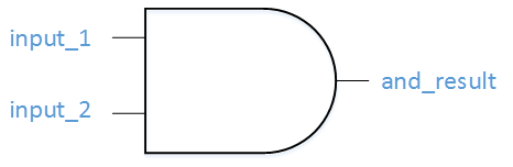
Verilog 구현으로 들어가 보겠습니다.
Verilog에서 빌딩 블록은 wire입니다. 이 예제에서는 와이어를 0 또는 1만 될 수 있는 이진 신호로 다룹니다.
wire and_temp; assign and_temp = input_1 & input_2;
첫 줄은 and_temp라는 와이어를 선언합니다. 두 번째 줄은 input_1과 input_2의 논리 AND 결과를 할당합니다. Verilog에서 앰퍼샌드(&)는 불리언 AND 연산자입니다.
모듈이 노출하는 모든 신호는 module 헤더에 나열됩니다. module 키워드는 정의된 입력과 출력을 가진 독립된 코드 블록을 도입합니다.
module example_and_gate ( input_1, input_2, and_result ); input input_1; input input_2; output and_result;
마지막으로 내부 and_temp 신호를 외부 and_result 출력에 연결하고 모듈을 닫습니다.
/////////////////////////////////////////////////////////////////////////////// // File Downloaded from https://www.nandland.com /////////////////////////////////////////////////////////////////////////////// module example_and_gate ( input_1, input_2, and_result ); input input_1; input input_2; output and_result; wire and_temp; assign and_temp = input_1 & input_2; assign and_result = and_temp; endmodule // example_and_gate
축하합니다—첫 Verilog 모듈을 작성했습니다! HDL 문법이 일반 소프트웨어에 비해 장황하게 느껴질 수 있지만, 하드웨어 설계에 비교할 수 없는 정밀도를 제공합니다. 연습하면 단순한 로직 게이트부터 풀 블로운 그래픽 파이프라인까지 구현할 수 있게 됩니다.