

나노물질

산업 제조
전자 증배수 이득은 발광층 물질의 2차 전자 방출 계수(SEE)와 밀접한 관련이 있습니다. SEE는 발광층의 두께와 밀접한 관련이 있습니다. 방출층이 얇은 경우 낮은 SEE는 전자 증배기의 낮은 이득을 유발합니다. 발광층이 두꺼우면 전도층이 발광층에 적시에 전하를 보충할 수 없으며 전자 증폭기 이득도 낮습니다. 전자 증배기는 일반적으로 Al2를 선택합니다. O3 및 높은 SEE 레벨 때문에 방출층으로서 MgO 필름. MgO Mg(OH)2로 용이한 조해 마그네슘2 (OH)2 CO3 및 MgCO3 결과적으로 SEE 수준이 낮아집니다. Al2의 SEE 레벨 O3 MgO보다 낮지만 Al2 O3 안정적이다. 우리는 물질의 SEE 준위를 테스트하기 위한 구형 시스템을 설계했으며 Al2의 SEE 준위를 측정하기 위해 중화를 위해 저에너지 전자빔 대신 저에너지 2차 전자를 사용할 것을 제안했습니다. O3 , MgO, MgO/Al2 O3 , Al2 O3 /MgO, 원자층 증착을 이용하여 막두께를 정밀하게 조절합니다. 우리는 인접한 입사 전자 에너지 하에서 SEE를 비교하여 재료의 SEE 값을 분할하고 SEE와 두께 사이의 관계에 대한 4가지 실험식을 얻을 것을 제안합니다. SEE를 감소시키는 주요 물질은 Mg2이기 때문에 (OH)2 CO3 및 MgCO3 , 우리는 물질의 조해성 깊이를 연구하기 위해 XPS로 측정된 C 원소 원자 농도를 사용합니다. 우리는 다층 재료의 SEE 해석을 위해 전이층의 개념을 사용할 것을 제안합니다. 실험과 계산을 통해 2–3nm Al2을 포함한 전자 증배기를 위한 새로운 방출층을 제시했습니다. O3 버퍼 층, 5-9nm MgO 본체 층, 1nm Al2 O3 보호층 또는 0.3nm Al2 O3 향상 레이어. 우리는 이 발광층을 마이크로채널 플레이트(MCP)에 준비하여 MCP의 이득을 크게 향상시켰습니다. 우리는 또한 이 새로운 방출층을 채널 전자 증배기와 별도의 전자 증배기에 적용할 수 있습니다.
물질의 2차 전자 방출 계수(SEE)는 방출된 2차 전자 수와 물질에 대한 입사 전자 수의 비율로 정의됩니다. 2차 전자의 응용 분야는 매우 넓으며, 주로 전자증식 분야, 물질 표면 조성 및 구조 분석 분야, 미세방전 억제 분야로 구분됩니다. 전자증배 분야에는 채널전자증배관(CEM), 마이크로채널판(MCP), 분리전자증배관, MPG(마이크로펄스건), 유전체창, 원자시계 등 [1,2,3,4,5, 6,7,8,9]. 재료 표면 조성 및 구조 분석 분야에는 투과전자현미경(TEM), 주사전자현미경(SEM), 오거전자분광계(AES), 전자회절계 등이 있다[10,11,12,13]. 미세방전 억제 분야에는 링가속기 내면의 전자운 문제, 우주에서 고전력 마이크로파 진공소자의 신뢰성과 수명, 고전력 마이크로파 소스의 유전체 창 파괴, 충전/ 우주선 표면의 방전 문제 등 [1, 14].
우리의 주요 연구 분야는 전자 증배의 응용 분야입니다. 전자 증배관은 기판, 전도층 및 방출층으로 구성됩니다. 입사 전자가 발광층에 부딪치면 발광층에서 2차 전자가 생성됩니다. 2차 전자는 바이어스 전압에 의해 더욱 가속되어 방출층을 공격하고 점점 더 많은 2차 전자를 유도하여 전자 눈사태를 일으키고 출력에서 전자 구름을 방출합니다. 방출층은 점점 더 많은 2차 전자로 인해 많은 양의 전하를 잃어버리므로 전자 방출의 손실을 위한 전도층은 지속적으로 전하를 제공한다[15].
SEE는 발광층의 두께와 밀접한 관련이 있습니다. 방출층이 얇은 경우 낮은 SEE는 전자 증배기의 낮은 이득을 유발합니다. 발광층이 두꺼우면 전도층이 전자 눈사태로 인해 발광층의 손실 전하를 적시에 보충할 수 없어 전자 증배기의 이득이 낮아집니다. 실험은 5 ~ 15nm 사이의 발광층이 적절하다는 것을 경험했습니다. 따라서 전자 증배수의 이득은 물질의 SEE 레벨 및 발광층의 두께와 밀접한 관련이 있습니다. 발광층의 두께와 물질의 SEE 수준을 연구하는 것이 매우 중요해집니다.
Al2의 SEE 레벨은 O3 매우 높다[16]. 따라서 Al2 O3 일반적으로 전자 증배관에서 방출층 필름으로 선택됩니다. 그러나 MgO의 SEE 수준은 Al2보다 훨씬 높습니다. O3 [2, 17]. MgO가 선택되지 않은 이유는 4가지입니다. 첫째, MgO는 Mg(OH)2로 쉽게 분해됩니다. 마그네슘2 (OH)2 CO3 및 MgCO3 , SEE 레벨이 Al2만큼 낮아집니다. O3 그림 1과 같이 둘째, 필름은 포화된 MgO SEE 수준에서 매우 두꺼워(35nm), 전도층이 제 시간에 방출층 표면에 전하를 보충할 수 없습니다. 세 번째, Al2의 속성 O3 대기에서 오랫동안 안정적입니다. 넷째, Al2의 준비 과정 O3 MgO보다 간단합니다. ALD(Atomic Layer Deposition)는 연속적인 no pin-microchannel 필름을 생성할 수 있고 우수한 적용 범위를 가지며 원자 필름 두께와 조성을 제어할 수 있습니다. 따라서 우리는 발광층의 두께를 연구하기 위한 중요한 준비 방법으로 ALD를 선택합니다[18,19,20,21].
<그림>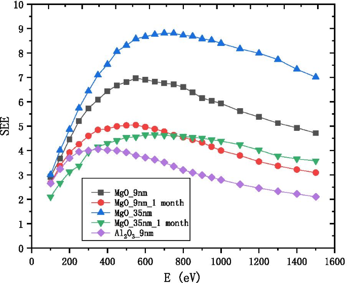
9nm-Al2의 SEE 변형 O3 입사 전자 에너지가 있는 9nm-MgO 및 35nm-MgO 및 샘플의 공기 조해 1개월 후 측정 결과
조해성 MgO의 최종 생성물은 주로 Mg2인 것으로 알려져 있습니다. (OH)2 CO3 및 MgCO3 , 따라서 재료의 다른 깊이에서 C 원자 농도의 함량은 MgO의 조해성 깊이를 반영할 수 있습니다. 표면은 Ar 이온 빔 스퍼터링으로 에칭되고 X선 광전자 분광법(XPS)으로 분석됩니다. 두 가지가 번갈아 수행됩니다. 에칭 시간을 제어하여 에칭 깊이를 제어하고, XPS에 의해 C 및 Mg 원소의 상대 원자 농도 백분율 변화를 얻습니다. XPS가 C 원소의 상대 농도 백분율을 측정할 수 없는 경우, 이 때의 에칭 깊이는 MgO의 조해 깊이입니다. 위의 방법은 MgO의 조해 깊이가 약 3.8nm 및 1nm Al2임을 보여줍니다. O3 MgO를 조해성으로부터 보호할 수 있습니다.
물질의 SEE 수준을 측정하기 위해 Stanford Linear Accelerator Center[14], University of Utah[22], Princeton University[23]; ONERA/DESP [24]; 중국 과학 기술 대학, Xi'an Jiaotong 대학, 504 항공 우주 연구소, 중국 파쇄 중성자 소스, 중국 전자 과학 기술 대학 등 우리는 재료의 SEE 수준을 테스트하기 위해 구형 시스템을 설계하여 다음을 보장합니다. 2차 전자의 전체 수집 및 측정 결과의 정확도 향상에 도움이 됩니다. 그리고 MgO, Al2와 같은 절연 물질의 SEE를 측정하기 위해 중성화를 위해 저에너지 전자빔 대신 저에너지 2차 전자를 사용하는 것이 좋습니다. O3 , 중화 용량과 중화 시간의 단점을 피할 수 있으므로[24, 25] 이 방법이 편리하고 비용이 저렴합니다.
집을 짓는다는 생각으로 전자 증배관의 발광층을 설계했고 좋은 결과를 얻었습니다. 우리는 이웃의 입사 전자 에너지 하에서 SEE 값을 비교하고 이것을 기준으로 재료를 저에너지 영역, 중간 에너지 영역 및 고에너지 영역으로 구분합니다. 이것은 미세방전을 억제하는 분야와 다르다[14]. 중간 에너지 영역은 SEE 값에 대한 입사 전자 에너지의 간섭을 제거할 수 있음을 알 수 있습니다. 따라서 중간 에너지 영역은 재료의 SEE 레벨을 측정하는 표준으로 선택되며 Al2 O3 , MgO, MgO/Al2 O3 , Al2 O3 /MgO는 실험식을 얻기 위해 연구됩니다.
현재 제안된 주요 SEE 물리적 모델은 Dionne 모델[26, 27]입니다. 제안된 이중층 모델[28]은 추가로 수정되었으며 현재 실험 데이터에는 적합하지 않습니다. 따라서 트랜지션 레이어의 개념을 사용하여 디자인의 재료 특성을 잘 설명할 수 있는 다층 재료를 설명하는 것이 좋습니다.
우리의 실험과 계산에 따르면 Al2를 성장시킨 후 O3 그런 다음 MgO를 성장시키면 이 필름이 MgO 필름보다 얇을 때 MgO의 포화된 SEE 수준이 드러날 수 있습니다. 이것은 MgO막이 너무 두꺼워 도전층이 발광층을 위한 전하를 보충할 수 없다는 문제를 해결한다. 그리고 우리는 MgO를 성장시킨 다음 Al2을 성장시킨 후에 O3 , Al2 O3 3nm 이상에서는 MgO의 SEE 수준이 더 이상 표시되지 않습니다. 1nm Al2 O3 MgO에 대한 외부 환경의 손상에 저항하고 MgO의 SEE 수준을 오랫동안 유지할 수 있습니다. 0.3nm Al2 O3 MgO의 포화 SEE 수준을 높일 수 있습니다. 따라서 우리는 새로운 발광층의 준비 과정이 2nm Al2 위에 9nm MgO 주층을 성장시키는 것이라고 제안합니다. O3 버퍼 층, 그 다음 1nm Al2 성장 O3 보호층 또는 0.3nm Al2 O3 전자 증배기에서 방출층의 MgO 결점 문제를 해결할 수 있는 강화층. 우리는 마이크로 채널 플레이트의 마이크로 채널(일종의 전자 증배기)에서 이 새로운 유형의 방출층을 성장시켜 마이크로 채널 플레이트의 이득을 크게 향상시켰습니다. 이 새로운 방출층의 설계 두께는 전자 증배기의 이득과 안정성을 향상시키는 데 매우 중요합니다.
ALD(Atomic Layer Deposition)는 전구체 가스와 반응 가스가 제어된 속도로 기저 표면에 교대로 들어가 표면에 물리적 또는 화학적 흡착 또는 표면 포화 반응이 발생하여 물질이 증착되는 기술의 일종입니다. 표면에 단일 원자막의 형태로 층별로. ALD는 연속적인 no pin-microchannel 필름을 생산할 수 있고 우수한 적용 범위를 가지며 원자 필름 두께 및 조성을 제어할 수 있습니다. 따라서 우리는 발광층의 두께를 연구하기 위한 중요한 준비 방법으로 ALD를 선택합니다.
다음은 ALD를 사용하여 Al2을 성장시키는 화학 반응식입니다. O3 :
$$\begin{정렬} {\text{A}} &:{\text{기판}} - {\text{OH}}^{*} + {\text{Al}}\left( {{\text {CH}}_{3} } \right)_{3} \to {\text{기판}} - {\text{O}} - {\text{Al}}\left( {{\text{CH }}_{3} } \right)_{2}^{*} + {\text{CH}}_{4} \uparrow \\ {\text{B}} &:{\text{기판}} - {\text{O}} - {\text{Al}}\left( {{\text{CH}}_{3} } \right)_{2}^{*} + 2{\text{H }}_{2} {\text{O}} \to {\text{기판}} - {\text{O}} - {\text{Al}}\left( {{\text{OH}}} \right)_{2}^{*} + 2{\text{CH}}_{4} \uparrow \\ {\text{C}} &:{\text{Al}} - {\text{OH }}^{*} + {\text{Al}}\left( {{\text{CH}}_{3} } \right)_{3} \to {\text{Al}} - {\text {O}} - {\text{Al}}\left( {{\text{CH}}_{3} } \right)_{2}^{*} + {\text{CH}}_{4 } \uparrow \\ {\text{D}} &:{\text{Al}} - {\text{CH}}_{3}^{*} + {\text{H}}_{2} { \text{O}} \to {\text{Al}} - {\text{OH}}^{*} + 2{\text{CH}}_{4} \uparrow \\ \end{정렬}$ $A와 B 또는 C와 D의 방정식이 보여주듯이 기저 표면은 원래 –OH로 덮여 있었고, –OH와 Al(CH3의 화학 반응) )3 (TMA)는 새로운 –CH3를 형성했습니다. 표면 및 릴리스 CH4 (부산물). 새로운 –CH3 수증기에 노출된 표면, 그들의 반응은 새로운 –OH 표면을 생성하고 CH4를 방출했습니다. 다시. 반응 온도는 200°C입니다. Al2 층을 성장시키는 시간과 순서 O3 그림 2와 같은 원자:
$${\text{TMA/N}}_{2} {\text{/H}}_{2} {\text{O/N}}_{2} =0.1\sim 1{\text{s }}/5\sim 45{\text{s}}/0.1\sim 1{\text{s }}/5\sim 45{\text{s}}{.}$$ <그림><소스 유형="image/webp" srcset="//media.springerature.com/lw685/springer-static/image/art%3A10.1186%2Fs11671-021-03606-y/MediaObjects/11671_2021_3606_Fig2_HTML.png?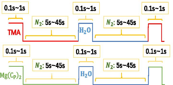
Al2 성장 과정의 개략도 O3 및 MgO
다음은 ALD를 사용하여 MgO를 성장시키는 화학 반응식입니다.
$$\begin{정렬} {\text{E}} &:{\text{기판}} - {\text{OH}}^{*} + {\text{Mg}}\left( {{\text {C}}_{5} {\text{H}}_{5} } \right)_{2} \to {\text{기질}} - {\text{O}} - {\text{MgC }}_{5} {\text{H}}_{5}^{*} + {\text{C}}_{5} {\text{H}}_{6} \uparrow \\ {\ text{F}} &:{\text{기질}} - {\text{O}} - {\text{MgC}}_{5} {\text{H}}_{5}^{*} + {\text{H}}_{2} {\text{O}} \to {\text{기판}} - {\text{OH}}^{*} + {\text{C}}_{5 } {\text{H}}_{6} \uparrow \\ {\text{G}} &:{\text{Mg}} - {\text{OH}}^{*} + {\text{Mg }}\left( {{\text{C}}_{5} {\text{H}}_{5} } \right)_{2} \to {\text{Mg}} - {\text{ O}} - {\text{MgC}}_{5} {\text{H}}_{5}^{*} + {\text{C}}_{5} {\text{H}}_ {6} \uparrow \\ {\text{H}} &:{\text{Mg}} - {\text{C}}_{5} {\text{H}}_{5}^{*} + {\text{H}}_{2} {\text{O}} \to {\text{Mg}} - {\text{OH}}^{*} + {\text{C}}_{ 5} {\text{H}}_{6} \uparrow \\ \end{정렬}$$E와 F 또는 G와 H의 방정식에서 볼 수 있듯이 기저 표면은 원래 \(- {\text{OH}}\)로 덮여 있었고, \(- {\text{OH}}\)의 화학 반응과 \({\text{Mg}}\left( {{\text{C}}_{5} {\text{H}}_{5} } \right)_{2}\)(\({\ text{Mg}}\left( {{\text{C}}_{{\text{P}}} } \right)_{2}\))는 새로운 \(- {\text{C}}를 형성했습니다. _{5} {\text{H}}_{5}\) 표면 및 릴리스된 \({\text{C}}_{5} {\text{H}}_{6}\) (부산물) . 수증기에 노출된 새로운 \(- {\text{C}}_{5} {\text{H}}_{5}\) 표면, 이들의 반응으로 새로운 \(- {\text{OH}} \) 표면 및 릴리스 \({\text{C}}_{5} {\text{H}}_{6}\) 다시.
우리는 \({\text{Mg}}\left( {{\text{C}}_{{\text{P}}} } \right)_{2}\)를 60°C로 가열하여 먼지. 반응 챔버의 온도는 200°C입니다. 그림 2와 같이 MgO 원자층을 성장시키는 시간과 순서:
$${\text{Mg}}\left( {{\text{Cp}}} \right)_{2} {\text{/N}}_{2} {\text{/H}}_{ 2} {\text{O/N}}_{2} =0.1\sim 1{\text{s}}/5\sim 45{\text{s}}/0.1\sim 1{\text{s } }/5\sim 45{\text{s}}{.}$$샘플은 그림 3과 같이 4가지 방법으로 준비됩니다. Si 웨이퍼에서 다른 두께의 MgO 성장; Si 웨이퍼에 서로 다른 두께의 \({\text{Al}}_{2} {\text{O}}_{3}\)를 성장시킨 다음 고정된 두께의 MgO를 성장시킵니다. Si 웨이퍼에 고정된 두께의 MgO를 성장시킨 다음 \({\text{Al}}_{2} {\text{O}}_{3}\)의 다른 두께를 성장시킵니다. Si 웨이퍼(1 nm, 3 nm, 7 nm, 9 nm, 30 nm)에서 서로 다른 두께의 \({\text{Al}}_{2} {\text{O}}_{3}\) 성장 , 50nm). 우리는 Si 웨이퍼(1nm, 3nm, 5nm, 9nm, 15nm, 20nm, 35nm)에 다양한 두께의 MgO를 성장시켰습니다. Si 웨이퍼(0.6nm, 1nm, 3nm, 30nm)에서 서로 다른 두께의 \({\text{Al}}_{2} {\text{O}}_{3}\)를 성장시킨 다음 성장합니다. MgO의 고정 두께(9nm). Si 웨이퍼(35nm)에 고정된 두께의 MgO를 성장시킨 다음 \({\text{Al}}_{2} {\text{O}의 다른 두께를 성장시킵니다. }_{3}\) (0.3nm, 0.6nm, 1nm, 3nm, 5nm, 7nm, 10nm, 20nm).
<그림>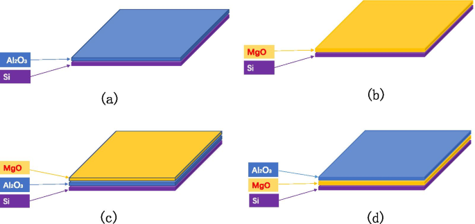
발광층 실험 설계를 통한 막두께와 SEE의 관계 연구
그림 4와 같이 컬렉터 방법을 사용하여 측정합니다. 먼저 샘플 스테이지를 컬렉터에 연결하고 피코 전류계로 측정한 전류는 \(I_{{\text{p}}}\로 표시되는 입사 전자 전류입니다. ); 동일한 조건에서 시료와 컬렉터를 분리합니다. 이때 컬렉터에서 측정된 전류는 \(I_{{\text{s}}}\)로 표시되는 2차 전자 전류입니다.
$${\text{SEE}} =\frac{{I_{{\text{s}}} }}{{I_{{\text{p}}} }}$$ <사진><소스 유형=" image/webp" srcset="//media.springerature.com/lw685/springer-static/image/art%3A10.1186%2Fs11671-021-03606-y/MediaObjects/11671_2021_3606_Fig4_HTML.p">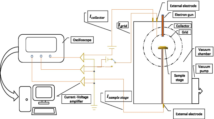
2차 전자 방출 효율 시스템의 개략도
2차 전자의 완전한 수집을 보장하고 측정 결과의 정확도를 향상시키는 데 도움이 되도록 장치를 전역 모양의 구조로 설계했습니다.
절연 물질이 입사 전자에 의해 충격을 받으면 물질 표면은 전자의 손실로 인해 2차 전자를 방출하고 양전하를 축적합니다. 양전하는 잠재적으로 상승합니다. 2차 전자는 재료 표면의 수 나노미터 내에서 생성되고 낮은 에너지(~ eV)를 갖기 때문입니다. 2차 전자는 양전위에 매우 민감합니다. 양전위는 다음 2차 전자 방출 과정에 영향을 주어 2차 전자 수율을 감소시킵니다.
절연 샘플의 SEE 측정 결과에 대한 전하 축적의 영향을 제거하고 절연 샘플의 SEE를 정확하게 측정하기 위해 기존의 방법은 저에너지 전자빔을 직접 사용하여 절연 샘플을 조사하고 양극 샘플 표면의 전하는 저에너지 전자에 의해 중화됩니다. 전통적인 방법에는 두 가지 단점이 있습니다. 첫째, 중화량을 정확하게 계산해야 하며, 중화량이 부족하여 시료 표면에 양전하를 띠거나 과도한 중화로 인해 시료 표면에 음전하를 띠기 쉽습니다. 둘째, 또 다른 하나의 저에너지 전자총을 장착해야 합니다[24, 25].
우리는 중화를 위해 저에너지 전자빔 대신 저에너지 2차 전자를 사용할 것을 제안한다. 이는 기존 방법의 단점을 극복하고 그림 5와 같이 정확한 2차 전자를 얻을 수 있다[29]. 테스트할 절연 샘플을 샘플 스테이지의 절반에 놓고 나머지 절반은 비워 둡니다. 샘플 테이블은 304 스테인리스 스틸로 만들어졌으며 전위는 0V입니다.
<그림>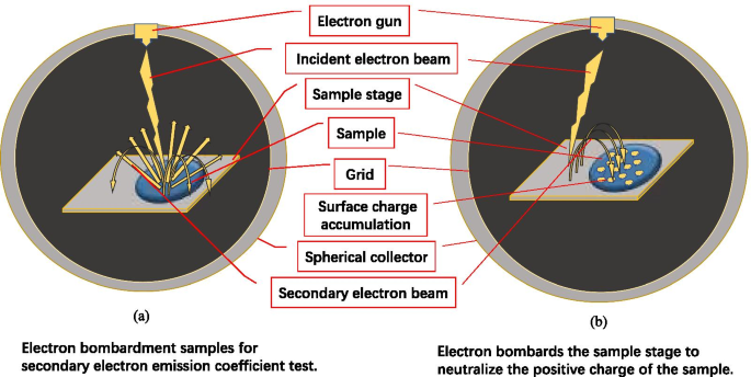
재료의 2차 전자 방출 계수에 대한 새로운 시험 방법의 개략도
절연성 시료를 테스트할 때 전자총에 의해 생성된 전자는 그림 5a와 같이 절연성 시료의 표면에 충돌하여 그림 5b와 같은 양전하 영역이 생성됩니다. 절연성 시료의 표면전하를 중화할 때 전자총의 각도를 조절하여 시료대의 절반 빈 영역에 충격을 가하여 시료단이 그림 5b와 같이 2차 전자를 방출하도록 한다.
양전하와 전자의 상호 인력으로 인해 2차 전자는 전하 중화를 위해 시료 표면으로 유인됩니다. 양전하가 감소함에 따라 더 적은 수의 전자가 끌립니다. 시료 표면의 양전하가 중화되면 절연 시료의 표면이 원래 상태로 돌아갑니다. 양전하가 없기 때문에 샘플 스테이지에서 생성된 저에너지 2차 전자를 계속 끌어들이지 않으므로 샘플 표면이 음으로 대전되는 과도한 중화가 발생하지 않습니다.
우리가 사용하는 전자총은 매번 같은 위치에서 샘플 표면에 충격을 가한 다음 그림 6과 같이 샘플 스테이지의 동일한 위치에 동일한 각도를 편향하여 충격을 가합니다. 장기 SEE 테스트 프로세스로 인해 위치는 샘플 스테이지에서 전자총에 의해 오랜 시간 충격을 받은 부분은 그림 6과 같이 검은 점이 되었습니다.
<그림>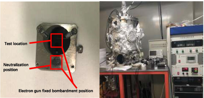
시료, 시료대, 2차전자방출계수 시험장비 사진
인접한 입사 전자 에너지에서 SEE 값을 비교하여 SEE의 변화를 입사 전자의 에너지로 설명하고 다음과 같이 정의합니다.
$$R_{{{\text{SEE}}}} =\frac{{{\text{SEE}}\left( {x + b } \right)}}{{{\text{SEE}}\left ( {x } \right)}}$$재료의 SEE는 \(R_{{{\text{SEE}}}}\) 값의 크기에 따라 세 영역, 즉 입사 전자의 낮은 에너지 영역(\(R_{{{ \text{SEE}}}} \ge 1.02\)), 입사 전자의 중간 에너지 영역(\(0.98 \le R_{{{\text{SEE}}}} <1.02\)) 및 고에너지 입사 전자의 영역(\({\text{R}}_{{{\text{SEE}}}} \ge 0.98\)). SEE 테스트에 사용하는 재료의 입사 전자 에너지 범위는 (100 eV, 1500 eV), x입니다. 입사 전자 에너지를 나타내고 b SEE 테스트에서 입사 전자 에너지의 단계 길이를 나타냅니다.
\({\text{Al}}_{2} {\text{O}}_{3}\) SEE는 기본적으로 그림 7과 같이 7nm 이후에 변하지 않습니다. 그림 7a, b에서 볼 수 있듯이, \({\text{Al}}_{2} {\text{O}}_{3}\)의 저에너지 영역은 100~250eV이며, \(R_{{{\text{SEE}} }}\)는 1.25에서 1.02로 감소하여 입사 전자 에너지가 증가함에 따라 SEE가 증가하고 최종적으로 안정화됨을 나타냅니다. 그림 7c, d에서 볼 수 있듯이 \({\text{Al}}_{2} {\text{O}}_{3}\)의 중간 에너지 영역은 250에서 500eV 사이이며, \( R_{{{\text{SEE}}}}\)는 [0.98, 1.02] 간격 내에서 일정한 것으로 간주됩니다. 즉, \(R_{{{\text{SEE}}}}\)는 거의 같습니다. 1로, 입사 전자 에너지가 증가함에 따라 SEE가 기본적으로 변하지 않음을 나타냅니다. 그림 7e, f에서 볼 수 있듯이 \({\text{Al}}_{2} {\text{O}}_{3}\)의 고에너지 영역은 모든 증가에 대해 500에서 1500eV 사이입니다. 200eV의 입사 전자 에너지에서 SEE는 약 0.9배 감소합니다.
<사진>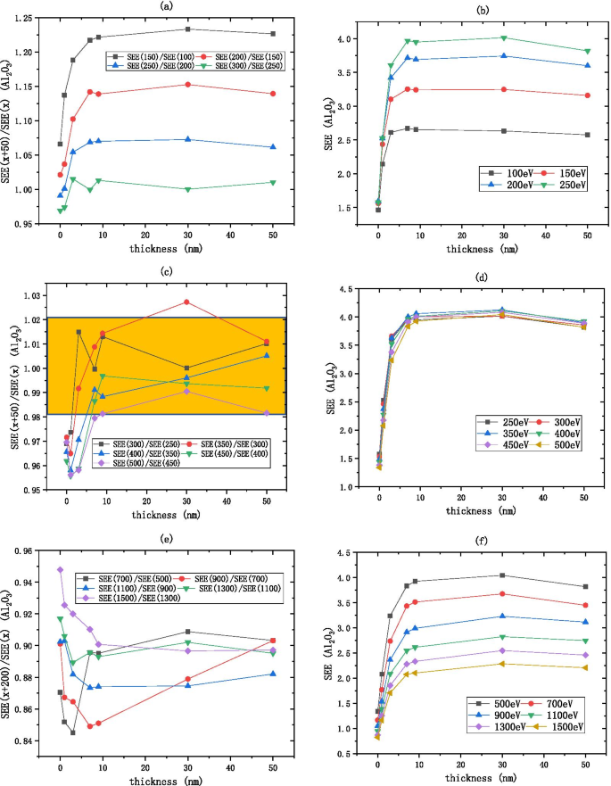
입사 전자 에너지를 \(R_{{{\text{SEE}}}} =\frac{{\text{SEE(x + b)}}}{{\text{SEE(x)}}}로 나눈 후 \) a에 표시된 대로 , ㄷ , e Al2의 변경 O3 (실리콘 웨이퍼에서 xnm-Al2 성장 O3 ) b에 표시된 대로 두께로 SEE , d , f
MgO SEE는 기본적으로 그림 9와 같이 20nm 후에도 변하지 않습니다. 그림 8a, b에서 볼 수 있듯이 MgO의 저에너지 영역은 100~500eV 사이이며, \(R_{{{\text{SEE} }}}\)는 1.3에서 1로 감소하여 입사 전자 에너지가 증가함에 따라 SEE가 증가하고 최종적으로 안정화됨을 나타냅니다. 그림 8c, d와 같이 MgO의 중간 에너지 영역은 500과 1000 eV 사이이고, \(R_{{{\text{SEE}}}}\)는 [0.98, 1.02 ], 즉 \(R_{{{\text{SEE}}}}\)는 대략 1과 같으며, 이는 입사 전자 에너지가 증가함에 따라 SEE가 기본적으로 변하지 않음을 나타냅니다. 그림 8e, f에서 볼 수 있듯이 MgO의 고에너지 영역은 1000~1500eV이며 입사 전자 에너지가 100eV 증가할 때마다 SEE가 약 0.94배 감소합니다.
<그림>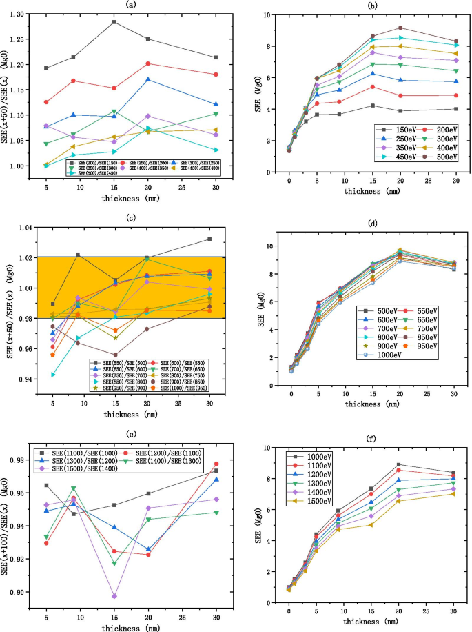
입사 전자 에너지를 \(R_{{{\text{SEE}}}} =\frac{{\text{SEE(x + b)}}}{{\text{SEE(x)}}}로 나눈 후 \) a에 표시된 대로 , ㄷ , e b와 같이 두께에 따른 MgO의 변화(실리콘 웨이퍼에서 xnm-MgO 성장) SEE , d , f
그림 9에서 볼 수 있듯이 \({\text{Al}}_{2} {\text{O}}_{3}\)/MgO와 MgO의 SEE는 유사한 입사 전자 에너지 파티션을 가지며, \({\text{Al}}_{2} {\text{O}}_{3}\)/MgO는 기본적으로 3nm 이후에 변하지 않습니다. 그림 9a, b에서 볼 수 있듯이 \({\text{Al}}_{2} {\text{O}}_{3}\)/MgO의 저에너지 영역은 100~450eV이며, \(R_{{{\text{SEE}}}}\) 는 1.4에서 1.05로 감소하여 입사 전자 에너지가 증가함에 따라 SEE가 증가하고 최종적으로 안정화됨을 나타냅니다. 그림 9c, d와 같이 \({\text{Al}}_{2} {\text{O}}_{3}\)/MgO의 중간 에너지 영역은 500에서 1000 eV 사이이며, \(R_{{{\text{SEE}}}}\)는 [0.98, 1.02] 간격 내에서 일정한 것으로 간주됩니다. 즉, \(R_{{{\text{SEE}}}}\)는 거의 1과 같으며, 입사 전자 에너지가 증가함에 따라 SEE가 기본적으로 변하지 않음을 나타냅니다. 그림 9e, f에서 볼 수 있듯이 \({\text{Al}}_{2} {\text{O}}_{3}\)/MgO의 고에너지 영역은 1000에서 1500 eV 사이입니다. 입사 전자 에너지가 100V 증가할 때마다 SEE는 약 0.95배 감소합니다. \({\text{Al}}_{2} {\text{O}}_{3}\)/MgO의 SEE는 중간 에너지 영역에서 안정적이므로 입사 전자 에너지를 변수로 제외할 수 있습니다. 요인.
<그림>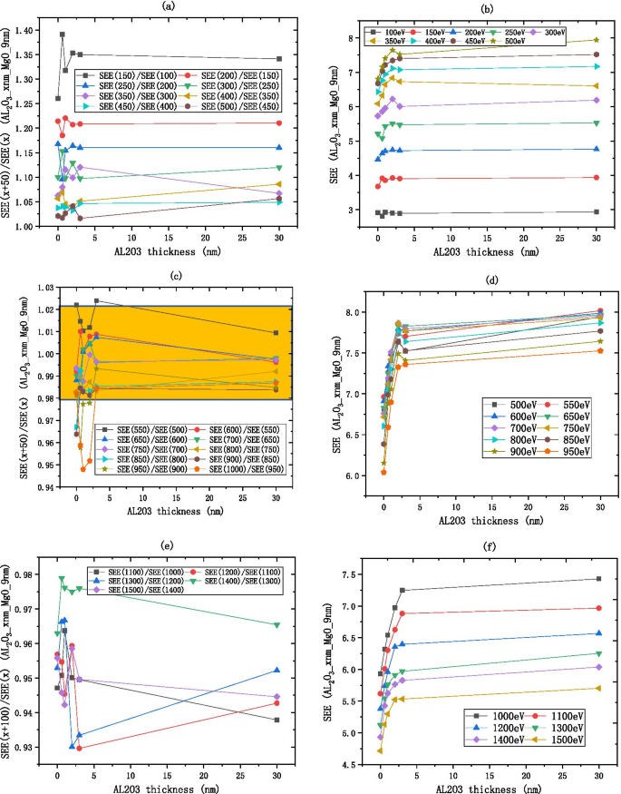
입사 전자 에너지를 \(R_{{{\text{SEE}}}} =\frac{{\text{SEE(x + b)}}}{{\text{SEE(x)}}}로 나눈 후 \) a에 표시된 대로 , ㄷ , e Al2의 변경 O3 /MgO(실리콘 웨이퍼에서 xnm-Al2 성장) O3 그런 다음 b와 같이 두께로 9nm-MgO) SEE를 성장시킵니다. , d , f
그림 10과 같이 MgO/\({\text{Al}}_{2} {\text{O}}_{3}\) 및 \({\text{Al}}_{ 2} {\text{O}}_{3}\) 유사한 입사 전자 에너지 파티션을 가지며, MgO/\({\text{Al}}_{2} {\text{O}}_{3 }\) 기본적으로 3nm 이후에는 변경되지 않습니다. 그림 10a, b에서 볼 수 있듯이 MgO/\({\text{Al}}_{2} {\text{O}}_{3}\)의 저에너지 영역은 100~300 eV이며, \(R_{{{\text{SEE}}}}\) 는 1.8에서 1로 감소하여 입사 전자 에너지가 증가함에 따라 SEE가 증가하고 최종적으로 안정화됨을 나타냅니다. 그림 10c, d와 같이 MgO/\({\text{Al}}_{2} {\text{O}}_{3}\)의 중간 에너지 영역은 300~500eV이며, \(R_{{{\text{SEE}}}}\)는 \({\text{Al}}_{2} {\text{O}}일 때 [0.98, 1.02] 간격 내에서 상수로 간주됩니다. _{3}\) 는 얇고 \(R_{{{\text{SEE}}}}\) 는 1에서 벗어나며, 다른 입사 전자 에너지에서 SEE의 차이는 분명합니다. \({\text{Al}}_{2} {\text{O}}_{3}\)가 두꺼운 경우 \(R_{{{\text{SEE}}}}\)는 1에 가까움 , 그리고 그 차이는 분명하지 않습니다. 그림 10e, f에서 볼 수 있듯이 MgO/\({\text{Al}}_{2} {\text{O}}_{3}\)의 고에너지 영역은 500에서 1500 eV 사이입니다. \({\text{Al}}_{2} {\text{O}}_{3}\)는 가늘고, \(R_{{{\text{SEE}}}}\)는 1에 가깝고, 다른 입사 전자 에너지에서 SEE의 차이는 분명하지 않습니다. \({\text{Al}}_{2} {\text{O}}_{3}\)가 두꺼울 때 \(R_{{{\text{SEE}}}}\)는 1에서 벗어나고, 그리고 그 차이는 분명합니다. 입사 전자 에너지가 200V 증가할 때마다 SEE는 약 0.9배 감소합니다.
<그림>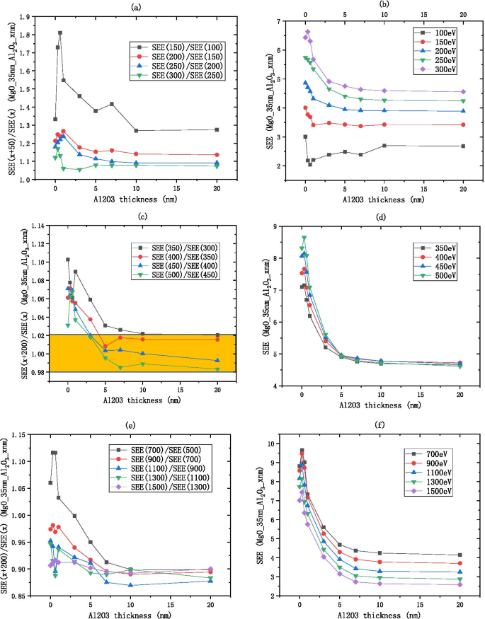
입사 전자 에너지를 \(R_{{{\text{SEE}}}} =\frac{{\text{SEE(x + b)}}}{{\text{SEE(x)}}}로 나눈 후 \) a, c, e와 같이 , MgO/Al2의 변화 O3 (실리콘 웨이퍼에서 35nm-MgO를 성장시킨 다음 xnm-Al2을 성장시킵니다. O3 ) b에 표시된 대로 두께로 SEE , d, f
\({\text{Al}}_{2} {\text{O}}_{3}\) SEE는 중간 에너지 영역에서 안정적이기 때문에 입사 전자 에너지는 가변 요인으로 제외될 수 있습니다. 실험 공식인 \({\text{Al}}_{2} {\text{O}}_{3}\)의 SEE 수준을 측정하기 위한 표준으로 중간 입사 전자 에너지 300eV를 선택했습니다. \({\text{Al}}_{2} {\text{O}}_{3}\)의 두께와 최상의 SEE는 그림 11a(표 1)와 같이 피팅하여 얻어집니다.
$${\text{B}}\_{\text{보기}}_{{{\text{Al}}_{2} {\text{O}}_{3} }} =3.99 - 2.5{ *}e^{{ - \frac{{{\text{두께}}}}{1.73}}}$$ (1)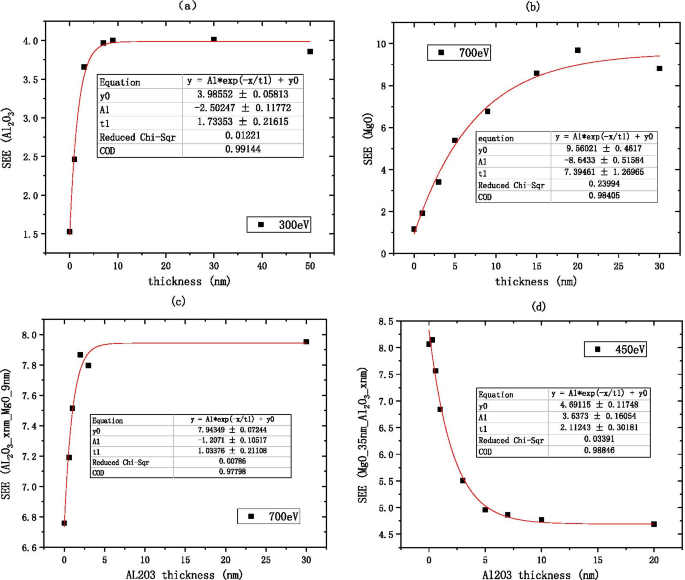
재료의 최상의 2차전자방출계수와 막두께의 관계 a shows the information of Al2 O3 (on the silicon wafer, grow xnm-Al2 O3 ), b shows the information of MgO (on the silicon wafer, grow xnm-MgO), c shows the information of Al2 O3 /MgO (on the silicon wafer, grow xnm-Al2 O3 , and then grow 9 nm-MgO), and d shows the information of MgO/Al2 O3 (on the silicon wafer, grow 35 nm-MgO, and then grow xnm-Al2 O3 )
Because the MgO SEE is stable in the medium energy region, the incident electron energy can be excluded as a variable factor. We choose the medium incident electron energy 700 eV as the standard to measure the SEE level of MgO, the empirical formula for the thickness of alumina material and the best SEE is obtained by fitting as shown in Fig. 11b.
$${\text{B}}\_{\text{SEE}}_{{{\text{MgO}}}} =9.56 - 8.64*e^{{ - \frac{{{\text{thickness}}}}{7.39}}}$$ (2)Because the SEE of \({\text{Al}}_{2} {\text{O}}_{3} /{\text{MgO}}\) is stable in the medium energy region, the incident electron energy can be excluded as a variable factor. We choose the medium incident electron energy 700 eV as the standard to measure the SEE level of \({\text{Al}}_{2} {\text{O}}_{3}\)/MgO, the empirical formula for the thickness of alumina material and the best SEE is obtained by fitting as shown in Fig. 11c.
$${\text{B}}\_{\text{SEE}}_{{{\text{Al}}_{2} {\text{O}}_{3} /{\text{MgO}}}} =7.94 - 1.21\,*\,e^{{ - \frac{{{\text{thickness}}}}{1.03}}}$$ (3)Because the SEE of MgO/\({\text{Al}}_{2} {\text{O}}_{3}\) is stable in the medium energy region, the incident electron energy can be excluded as a variable factor. We choose the medium incident electron energy 450 eV as the standard to measure the SEE level of MgO/\({\text{Al}}_{2} {\text{O}}_{3}\), the empirical formula for the thickness of alumina material and the best SEE is obtained by fitting as shown in Fig. 11d.
$${\text{B}}\_{\text{SEE}}_{{{\text{MgO}}/{\text{Al}}_{2} {\text{O}}_{3} }} =4.69 + 3.64\,*\,e^{{ - \frac{{{\text{thickness}}}}{2.11}}}$$ (4) $$\frac{{{\text{B}}\_{\text{SEE}}_{{{\text{MgO}}}} \left( 9 \right)}}{{{\text{B}}\_{\text{SEE}}_{{{\text{Al}}_{2} {\text{O}}_{3} }} \left( {30} \right)}} =\frac{{9.56 - 8.64\,*\,e^{{ - \frac{9}{7.39}}} }}{{3.99 - 2.5\,*\,e^{{ - \frac{30}{{1.73}}}} }} \approx 1.755$$According to formulas 1 and 2, the SEE level of 9 nm MgO is 1.755 times higher than that of 30 nm \({\text{Al}}_{2} {\text{O}}_{3}\).
$$\begin{aligned} \frac{{{\text{B}}\_{\text{SEE}}_{{{\text{Al}}_{2} {\text{O}}_{3} /{\text{MgO}}}} \left( 3 \right)}}{{{\text{B}}\_{\text{SEE}}_{{{\text{Al}}_{2} {\text{O}}_{3} }} \left( {30} \right)}} &=\frac{{7.94 - 1.21\,*\,e^{{ - \frac{3}{{1.03}}}} }}{{3.99 - 2.5\,*\,e^{{ - \frac{{30}}{{1.73}}}} }} \approx 1.973 \\ \frac{{{\text{B}}\_{\text{SEE}}_{{{\text{Al}}_{2} {\text{O}}_{3} /{\text{MgO}}}} \left( 3 \right)}}{{{\text{B}}_{{{\text{SEE}}\,{\text{MgO}}}} \left( 9 \right)}} &=\frac{{7.94 - 1.21\,*\,e^{{ - \frac{3}{{1.03}}}} }}{{9.56 - 8.64\,*\,e^{{ - \frac{9}{{7.39}}}} }} \approx 1.124 \\ \end{aligned}$$We deposit 0–30 nm \({\text{Al}}_{2} {\text{O}}_{3}\) and redeposit 9 nm MgO on the Si wafer as the film, as shown in Fig. 12a. formulas 1 and 3 show that the SEE level of 9 nm MgO grown on 3 nm \({\text{Al}}_{2} {\text{O}}_{3}\) is 1.973 times higher than that of \({\text{Al}}_{2} {\text{O}}_{3}\). formulas 2 and 3 show that the SEE level of 9 nm MgO grown on 3 nm \({\text{Al}}_{2} {\text{O}}_{3}\) is 1.124 times higher than that of 9 nm MgO.
$$\frac{{{\text{B}}\_{\text{SEE}}_{{{\text{MgO}}/{\text{Al}}_{2} {\text{O}}_{3} }} }}{{{\text{B}}\_{\text{SEE}}_{{{\text{Al}}_{2} {\text{O}}_{3} }} }} =\frac{{4.69 + 3.64\,*\,e^{{ - \frac{1}{2.11}}} }}{{3.99 - 2.5\,*\,e^{{ - \frac{30}{{1.73}}}} }} \approx 1.743$$
Change of secondary electron emission coefficient with different incident electron energy, a shows the information of Al2 O3 /MgO (on the silicon wafer, grow xnm-Al2 O3 , and then grow 9 nm-MgO), b shows the information of MgO/Al2 O3 and deliquescent MgO/Al2 O3 (on the silicon wafer, grow 35 nm-MgO, and then grow 1 nm-Al2 O3 ), c shows the information of MgO/Al2 O3 (on the silicon wafer, grow 35 nm-MgO, and then grow 0.3 nm-Al2 O3 ), and d shows the information of Al2 O3 /MgO (on the silicon wafer, grow 3 nm-Al2 O3 , and then grow 5 nm-MgO)
The SEE level of MgO after deliquescent drops significantly as shown in Fig. 1. Then, we deposit 35 nm MgO and redeposit 1 nm \({\text{Al}}_{2} {\text{O}}_{3}\) on the Si wafer as the film. We found the SEE of this film exposed to the air 7 months is close to the SEE without exposed to the air as shown in Fig. 12b. Formulas 1 and 3 show that the SEE level of 1 nm \({\text{Al}}_{2} {\text{O}}_{3}\) grown on MgO is 1.743 times higher than the SEE of \({\text{Al}}_{2} {\text{O}}_{3}\) and can be long-term maintain a high SEE level (no obvious deliquescence in 7 months).
$$\begin{aligned} \frac{{{\text{B}}\_{\text{SEE}}_{{{\text{MgO}}/{\text{Al}}_{2} {\text{O}}_{3} }} \left( {0.3} \right)}}{{{\text{B}}\_{\text{SEE}}_{{{\text{Al}}_{2} {\text{O}}_{3} }} \left( {30} \right)}} &=\frac{{4.69 + 3.64\,*\,e^{{ - \frac{0.3}{{2.11}}}} }}{{3.99 - 2.5\,*\,e^{{ - \frac{30}{{1.73}}}} }} \approx 1.967, \\ \frac{{{\text{B}}\_{\text{SEE}}_{{{\text{MgO}}/{\text{Al}}_{2} {\text{O}}_{3} }} \left( {0.3} \right)}}{{{\text{B}}\_{\text{SEE}}_{{{\text{MgO}}}} \left( 9 \right)}} &=\frac{{4.69 + 3.64\,*\,e^{{ - \frac{0.3}{{2.11}}}} }}{{9.56 - 8.64\,*\,e^{{ - \frac{9}{7.39}}} }} \approx 1.12 \\ \end{aligned}$$We deposited 35 nm MgO on the Si wafer and re-deposited 0.3 nm \({\text{Al}}_{2} {\text{O}}_{3}\) as a thin film as shown in Fig. 12c. It can be seen from formulas 1, 2 and 4 that the SEE level of 0.3 nm \({\text{Al}}_{2} {\text{O}}_{3}\) grown on MgO is 1.967 times higher than that of \({\text{Al}}_{2} {\text{O}}_{3}\) and 1.12 times higher than that of MgO;
The emission layer of the electron multiplier pursues thinner and higher SEE level, so we sacrificed some SEE level to make the film thinner. We deposited 3 nm \({\text{Al}}_{2} {\text{O}}_{3}\) on the Si wafer and re-deposited 5 nm MgO as a thin film as shown in Fig. 12d.
We propose to grow 2–3 nm \({\text{Al}}_{2} {\text{O}}_{3}\) as a buffer layer, grow 5–9 nm MgO as the main layer, and grow 0.3 nm \({\text{Al}}_{2} {\text{O}}_{3}\) as an enhancement layer or 1 nm \({\text{Al}}_{2} {\text{O}}_{3}\) as a protective layer as the \({\text{Al}}_{2} {\text{O}}_{3}\)/MgO/\({\text{Al}}_{2} {\text{O}}_{3}\) emissive layer of electron multipliers as shown in Fig. 13. SEE level of \({\text{Al}}_{2} {\text{O}}_{3}\)/MgO/\({\text{Al}}_{2} {\text{O}}_{3}\) emission layer (\({\text{Al}}_{2} {\text{O}}_{3}\)/MgO/\({\text{Al}}_{2} {\text{O}}_{3}\) = 3 nm/9 nm/0.3 nm) is shown in Fig. 12a. And, we tested a traditional microchannel plate with good gain and then grew \({\text{Al}}_{2} {\text{O}}_{3}\)/MgO/\({\text{Al}}_{2} {\text{O}}_{3}\) emission layer on microchannel wall of microchannel plate, and the gain result obtained by the test was significantly improved. Then, another piece of the first convention microchannel plate with close gain is grown with \({\text{Al}}_{2} {\text{O}}_{3}\) emission layer. Compared with the gain results obtained by the test, the \({\text{Al}}_{2} {\text{O}}_{3}\)/MgO/\({\text{Al}}_{2} {\text{O}}_{3}\) emission layer structure is more superior as shown in Fig. 14.

Schematic diagram of sandwich structure (Al2 O3 /MgO/Al2 O3 )

Relationship between the voltage and gain of the three microchannel plates (conventional microchannel plate, microchannel plate for growing Al2 O3 emission layer, microchannel plate for growing Al2 O3 /MgO/Al2 O3 emission layer)
SEE data usually uses Dionne model for fitting analysis [26, 27]. The current double-layer model based on Dionne model does not consider the existence of a transition layer between the two materials. Through the design of the emission layer structure this time, the SEE difference between \({\text{Al}}_{2} {\text{O}}_{3}\)/MgO and \({\text{Si}}\)/MgO can be clearly observed. Under the same SEE level, MgO exhibits a very large thickness difference. Sample (0.3 nm \({\text{Al}}_{2} {\text{O}}_{3}\) grown on MgO) can get a higher SEE than MgO. Sample (1 nm \({\text{Al}}_{2} {\text{O}}_{3}\) grown on MgO) maintain a high SEE level. The current double-layer model [28] can no longer explain the above phenomenon, so we put forward the concept of transition layer, there are two kinds of materials at the interface, forming two processes:the process of destroying the bottom material and the process of building the top material. The following are two X-ray photoelectron spectroscopy (XPS) test experiments to prove and the concept of transition layer to understand the SEE phenomenon of multilayer materials.
XPS test experiment 1:
First, the sample (0.3 nm \({\text{Al}}_{2} {\text{O}}_{3}\) grown on MgO) in the air for 1 year are tested for XPS as shown in Fig. 15a. We use an Ar ion gun to etch the surface of the material, and then test the various elements in the material by XPS. The two are alternately performed. The etching depth is controlled by controlling the etching time, and the relative atomic concentration percentage changes of various elements are obtained by XPS. Al element is almost undetectable after 8 s of etching as shown in Fig. 16a. The etching rate of \({\text{Al}}_{2} {\text{O}}_{3}\) is known, \({\text{Etching}}\,{\text{rate}}_{{{\text{Al}}_{2} {\text{O}}_{3} }} =0.7{\text{{\AA}/s}}\),
$$\begin{aligned} &{\text{Etching}}\_{\text{Thickness}}_{{{\text{Al}}_{2} {\text{O}}_{3} }} ={\text{Etching rate }}_{{{\text{Al}}_{2} {\text{O}}_{3} }} *{\text{Etching time}}_{{{\text{Al}}_{2} {\text{O}}_{3} }} =0.7\,{\text{{\AA}/s}}\,*\,8\,{\text{s}} =5.6{\text{\AA}} \\ &{\text{Cycle}}\_{\text{Thickness}}_{{{\text{Al}}_{2} {\text{O}}_{3} }} =1.29\,{\text{{\AA}/cycle}}\,*3\,{\text{cycle}} =3.87{\text{\AA}} \\ &{\text{Etching}}\_{\text{Thickness}}_{{{\text{Al}}_{2} {\text{O}}_{3} }}> {\text{Cycle}}\_{\text{Thickness}}_{{{\text{Al}}_{2} {\text{O}}_{3} }} \\ \end{aligned}$$
Schematic diagram of XPS test experiment sample, a shows the information of MgO/Al2 O3 (on the silicon wafer, grow 35 nm-MgO, and then grow 0.3 nm-Al2 O3 ), b shows the information of deliquescent MgO/Al2 O3 (on the silicon wafer, grow 35 nm-MgO, and then grow 0.3 nm-Al2 O3 ), c shows the information of deliquescent MgO (on the silicon wafer, grow 11 nm-MgO), d shows the information of deliquescent MgO/Al2 O3 (on the silicon wafer, grow 35 nm-MgO, and then grow 1 nm-Al2 O3 )

Atomic concentration percentage of C, Al, Si elements relative to Mg element obtained by XPS. 아 Shows the Al element information of deliquescent MgO/Al2 O3 (on the silicon wafer, grow 35 nm-MgO, and then grow 0.3 nm-Al2 O3 ), a shows the C element information of deliquescent MgO/Al2 O3 (on the silicon wafer, grow 35 nm-MgO, and then grow 0.3 nm-Al2 O3 ), c shows the C element information of deliquescent MgO (on the silicon wafer, grow 11 nm-MgO), d shows the Si element information of deliquescent MgO (on the silicon wafer, grow 11 nm-MgO), e shows the C element information of deliquescent MgO/Al2 O3 (on the silicon wafer, grow 35 nm-MgO, and then grow 1 nm-Al2 O3 ). 에 shows the Al element information of deliquescent MgO/Al2 O3 (on the silicon wafer, grow 35 nm-MgO, and then grow 1 nm-Al2 O3 )
Therefore, it shows that \({\text{Al}}_{2} {\text{O}}_{3}\) must exist in the MgO part, that is, \({\text{Al}}_{2} {\text{O}}_{3}\) destroys the lattice state of the MgO surface. \({\text{Al}}_{2} {\text{O}}_{3}\) forms a finite solid solution in MgO [30]. At this time, the experimentally measured SEE level increased. As we all know, the higher the SEE level, the better the insulation of the material. Due to the destruction of the surface lattice, the surface layer of MgO is more insulating, which further confirms the process of destroying the underlying material in the concept of the transition layer.
According to the results of the SEE experiment, the SEE level has dropped significantly. A small amount of \({\text{Al}}_{2} {\text{O}}_{3}\) in the top layer cannot protect the MgO in the bottom layer. MgO is still deliquescent in the air. The air contains \({\text{O}}_{2} ,{\text{H}}_{2} {\text{O}},{\text{CO}}_{2} ,{\text{CO}},{\text{N}}_{2}\), etc. When air enters MgO, the reaction of MgO and \({\text{CO}}_{2}\) and \({\text{H}}_{2} {\text{O}}\) proceeds at the same time.
$$\begin{aligned} &{\text{MgO}} + {\text{H}}_{2} {\text{O}} ={\text{Mg}}\left( {{\text{OH}}} \right)_{2} \\ &{\text{MgO}} + {\text{CO}}_{2} ={\text{MgCO}}_{3} \\ &{\text{Mg}}\left( {{\text{OH}}} \right)_{2} + {\text{CO}}_{2} \rightleftharpoons {\text{MgCO}}_{3} + {\text{H}}_{2} {\text{O}} \\ &2{\text{MgO}} + 2{\text{H}}_{2} {\text{O}} + {\text{CO}}_{2} ={\text{Mg}}_{2} \left( {{\text{OH}}} \right)_{2} {\text{CO}}_{3} \\ \end{aligned}$$The above four chemical reactions occur, the deliquescent reaction of air and MgO is mainly the reaction of MgO and \({\text{CO}}_{2}\) and \({\text{H}}_{2} {\text{O}}\) to produce \({\text{MgCO}}_{3}\) and \({\text{Mg}}_{2} \left( {{\text{OH}}} \right)_{2} {\text{CO}}_{3}\). As long as the prepared MgO is exposed to the air, \({\text{Mg}}\left( {{\text{OH}}} \right)_{2}\) will be produced. After being placed in the air for 28 days, \({\text{MgCO}}_{3}\) is the main product [31]. Because the tested MgO sample needs to be transferred to the SEE test equipment, the actual test is the SEE level of MgO–\({\text{Mg}}\left( {{\text{OH}}} \right)_{2}\). Main reason for the decrease in SEE level is the \({\text{Mg}}_{2} \left( {{\text{OH}}} \right)_{2} {\text{CO}}_{3}\) and MgCO3 produced by deliquescent. Therefore, when using XPS, C can be selected as the calibration element for the deliquescent depth of MgO in the air. As shown in Fig. 16b, after 8 s of etching, no Al content is detected, but C content is still detected, indicating that the MgO in the bottom layer continues to deliquesce and is not protected by a small amount of \({\text{Al}}_{2} {\text{O}}_{3}\) as shown in Fig. 15b.
XPS test experiment 2:
First, the MgO sample in the air for 1 year are tested for XPS. After 1 min of etching, there was almost no C element as shown in Fig. 16c, indicating that the thickness of the dense \({\text{Mg}}_{2} \left( {{\text{OH}}} \right)_{2} {\text{CO}}_{3}\) film formed was the thickness of 1 min of etching.
After etching for 3 min, the sample begins to show Si element as shown in Fig. 16d, the etching rate of MgO and the thickness of \({\text{Mg}}_{2} \left( {{\text{OH}}} \right)_{2} {\text{CO}}_{3}\) film can be calculated through these data.
$$\begin{aligned} &{\text{Etching rate }}_{{{\text{MgO}}}} =\frac{{{\text{Thickness}}_{{{\text{MgO}}}} }}{{{\text{Etching time}}_{{{\text{MgO}}}} }} =\frac{{11.58\,{\text{nm}}}}{{180\,{\text{s}}}} =0.643{\text{{\AA}/s}} \\ &{\text{Etching}}\_{\text{Thickness}}_{{{\text{Mg}}_{2} \left( {{\text{OH}}} \right)_{2} {\text{CO}}_{3} }} \approx {\text{Etching}}\_{\text{Thickness}}_{{{\text{MgO}}}} \\ &\quad ={\text{Etching rate }}_{{{\text{MgO}}}} \,*\,{\text{Etching time}}_{{{\text{MgO}}}} =0.643{\text{\AA}}/{\text{s*}}60\,{\text{s}} \approx 3.85\,{\text{nm}} \\ \end{aligned}$$The 3.85 nm \({\text{Mg}}_{2} \left( {{\text{OH}}} \right)_{2} {\text{CO}}_{3}\) film layer acts as an air barrier layer to prevent further deliquescent of deep MgO as shown in Fig. 15c.
When 1 nm \({\text{Al}}_{2} {\text{O}}_{3}\) is grown on MgO, the XPS test data show that there is basically no C content and no Al content in the sample after the etching time of 14 s as shown in Fig. 16e, f.
$${\text{Etching}}\_{\text{Thickness}}_{{{\text{Al}}_{2} {\text{O}}_{3} }} ={\text{Etching rate }}_{{{\text{Al}}_{2} {\text{O}}_{3} }}* {\text{Etching time}}_{{{\text{Al}}_{2} {\text{O}}_{3} }} =0.7\,{\text{{\AA}/s}}\,*\,14\,{\text{s}} =9.8{\text{\AA}}$$It can be known by testing the C content that the depth of air penetration into the material is about 1 nm at this time. According to the concept of the transition layer, there are two kinds of materials at the interface to form the process of destroying the bottom layer material and constructing the top layer material. At the interface, \({\text{Al}}_{2} {\text{O}}_{3}\) destroys the crystal lattice on the surface of MgO. In order to prevent excessive infiltration of air, a complete \({\text{Al}}_{2} {\text{O}}_{3}\) atomic level is formed at least at 1 nm. When a complete \({\text{Al}}_{2} {\text{O}}_{3}\) atomic layer is not formed, the infiltration of air into the material cannot be prevented as in Example 1 above. The \({\text{Al}}_{2} {\text{O}}_{3}\) and \({\text{ Mg}}_{2} \left( {{\text{OH}}} \right)_{2} {\text{CO}}_{3}\) in the inner layer are mixed to help MgO form a dense air barrier layer in advance as shown in Fig. 15d.
The concept of transition layer understands the SEE phenomenon of multilayer materials:
The schematic diagram shown in Fig. 17a shows the concept of the transition layer, The thickness of the top layer material is \(d_{1}\), the thickness of the bottom layer material is \(d_{2}\) and the thickness of the transition layer is \(d_{1\sim 2}\).The schematic diagram is shown in Fig. 17b, c when there is enough thick \({\text{Al}}_{2} {\text{O}}_{3}\) or MgO, the incident electron depth is \(d_{{{\text{max}}\_1}}\), and there is no transition layer between \({\text{Al}}_{2} {\text{O}}_{3}\) and \({\text{Al}}_{2} {\text{O}}_{3}\) (there is no transition layer between MgO and MgO), that is, the thickness of the transition layer is 0. Through XPS test experiment 2, we get that the thickness of the transition layer between MgO and \({\text{Al}}_{2} {\text{O}}_{3}\) is 1 nm as shown in Fig. 17d, e.

아 Schematic diagram of the transition layer of the double layer structure, b schematic diagram of the Al2 O3 transition layer and incident electron depth, c schematic diagram of the MgO transition layer and incident electron depth, d schematic diagram of the Al2 O3 /MgO transition layer, e schematic diagram of the MgO/Al2 O3 transition layer
When the top layer material in the double-layer structure is MgO, the thickness of the MgO that reaches the saturated SEE level is different when the bottom layer material is different. If electrons are incident on the bottom layer material, the SEE level of the bottom layer material is low and cannot reach the saturated SEE level. Therefore, to reach the saturation SEE level, a complete MgO incident electron path needs to be formed. When the bottom layer material is different, such as Si or \({\text{Al}}_{2} {\text{O}}_{3}\), the thickness of the transition layer will be different, so the top layer MgO shows a different thickness.
It is found through experiments that a sample that grows 2 nm \({\text{Al}}_{2} {\text{O}}_{3}\) on a Si wafer and then grows 15 nm MgO can reach the SEE level of MgO saturation. Knowing that the thickness of the MgO–\({\text{Al}}_{2} {\text{O}}_{3}\) transition layer is 1 nm, it can be inferred that the thickness of the \({\text{Al}}_{2} {\text{O}}_{3}\)–Si transition layer is 1 nm, and the maximum depth of incident electrons of MgO is 14 nm as shown in Fig. 18a. It is found through experiments that the sample of 20 nm MgO grown on the Si wafer can reach the SEE level of MgO saturation. It has been inferred that the maximum depth of incident electrons of MgO is 14 nm, so the thickness of the MgO–Si transition layer can be calculated to be 6 nm as shown in Fig. 18b. Therefore, it can be explained that the SEE level of growing 2 nm \({\text{Al}}_{2} {\text{O}}_{3}\) on Si wafer and then growing 9 nm MgO is higher than the SEE level of 9 nm MgO growing on Si wafer. This is because the thickness of the MgO–\({\text{Al}}_{2} {\text{O}}_{3}\) transition layer is thinner than that of the MgO–Si transition layer. The actual MgO thickness of 8 nm involved in incident electrons is much thicker than 3 nm as shown in Fig. 18c, d.

Schematic diagram of the thickness of each layer of a multilayer structure, a shows the thickness of Al2 O3 /MgO (on the silicon wafer, grow 2 nm-Al2 O3 , and then grow 15 nm-MgO), b shows the thickness of MgO (on the silicon wafer, grow 20 nm-MgO), c shows the thickness of Al2 O3 /MgO (on the silicon wafer, grow 2 nm-Al2 O3 , and then grow 9 nm-MgO), d shows the thickness of MgO (on the silicon wafer, grow 9 nm-MgO)
It can be seen through experiments that growing 7 nm \({\text{Al}}_{2} {\text{O}}_{3}\) on Si wafers can reach the SEE level of \({\text{Al}}_{2} {\text{O}}_{3}\) saturation, so it can be calculated that the maximum depth of incident electrons of \({\text{Al}}_{2} {\text{O}}_{3}\) is 6 nm; growing 7 nm \({\text{Al}}_{2} {\text{O}}_{3}\) on 35 nm MgO can reach the SEE level of \({\text{Al}}_{2} {\text{O}}_{3}\) saturation, the thickness of the MgO-\({\text{Al}}_{2} {\text{O}}_{3}\) transition layer is 1 nm, and the maximum depth of incident electrons of \({\text{Al}}_{2} {\text{O}}_{3}\) is calculated again to be confirmed by 6 nm, as shown in Fig. 19a, b.

Schematic diagram of the thickness of each layer of a multilayer structure, a shows the thickness of Al2 O3 (on the silicon wafer, grow 7 nm-Al2 O3 ), b shows the thickness of MgO/Al2 O3 (on the silicon wafer, grow 20 nm-MgO, and then grow 7 nm-Al2 O3 )
In conclusion, we designed a global-shaped structure device for testing the SEE of the material and propose to use low-energy secondary electrons instead of low-energy electron beam for neutralization to measure the insulating material. We designed the emission layer of the electron multiplier with the idea of building a house to study the relationship between \({\text{Al}}_{2} {\text{O}}_{3}\) and MgO. We propose the nearest neighbor SEE ratio and use this to divide the SEE incident electron energy of the material into the high-energy region, the middle-energy region and the low-energy region. We have obtained four empirical formulas for SEE and thickness by studying \({\text{Al}}_{2} {\text{O}}_{3}\), MgO, MgO/\({\text{Al}}_{2} {\text{O}}_{3}\),\({\text{ Al}}_{2} {\text{O}}_{3}\)/MgO. We propose to use the concept of transition layer for SEE interpretation of multilayer materials and obtained the optimal \({\text{Al}}_{2} {\text{O}}_{3}\)/MgO/\({\text{Al}}_{2} {\text{O}}_{3}\) three-layer structure thickness suitable for electron multiplier through formula analysis and experimental experience. The thin film with this structure can maintain a high SEE level for a long time. This new emission layer will have broad application prospects in the channel electron multiplier (CEM), microchannel plate (MCP), independent electron multiplier and other devices.
The authors do not wish to share their data. Because the authors have academic competition with other institutions. The authors want to protect their academic achievements and seek research funding for future research.
나노물질
판금 설계 소개 주위를 둘러보면 판금으로 만든 제품이 많다는 것을 알게 될 것입니다. 음료수 캔, 조리기구, 파일 캐비닛과 같은 소비재 또는 차체, 프레임 및 배기 장치와 같은 산업 제품이 될 수 있습니다. 판금은 산업 및 소량 생산에 중요한 자산입니다. 따라서 이 문서는 판금 설계 기본 사항과 판금 설계자를 위한 몇 가지 유용한 팁에 대해 설명합니다. 많은 산업에서 제조 가능성을 위한 설계 또는 일반적으로 DFM으로 알려진 개념을 채택하고 있습니다. 판금 설계 산업에서 DFM은 판금 두께 차트 및 선행 계산을 기반으로 제조 리드
FDM 3D 프린터의 기능적 부분에 대해 이야기할 때 레이어 팬은 가장 중요한 구성 요소 중 하나입니다 찾을 수 있습니다. 3D 프린터에는 일반적으로 HotEnd 영역에 두 개의 팬이 있습니다. 하나는 HotEnd 디퓨저 냉각을 담당하고 다른 하나는 노즐에서 나오는 재료를 냉각합니다. 이 기사에서는 후자인 레이어 팬에 대해 이야기하겠습니다. 필요한 경우 모든 사용자는 노즐이 동일한 영역에서 지속적으로 움직이는 작은 영역 영역으로 일부 부품을 인쇄하려고 시도했으며, 이는 부품을 연화시키는 과도한 온도를 유발하는 프로세스입니다. 같