

산업기술

산업 제조
구리 PCB에서 PCB에 몇 가지 가능한 문제가 발생할 수 있지만 PCB 오류로 이어지는 4가지 일반적인 원인이 있다고 말할 수 있습니다.
1. 탄 부품.
2. 제대로 제조되지 않은 부품.
3. 환경적 요인.
4. 나이.
구리 PCB는 이러한 실패의 규칙성을 해결하거나 줄이기 때문에 주로 사용됩니다. 나무와 유리 PCB의 경우 납땜 인두 온도가 더 높으면 부품이 번트할 수 있으므로 어느 정도 완벽한지 확인해야 합니다.
구리 PCB는 필요한 재료와 쉽게 사용할 수 있도록 하는 조립 서비스로 만들 수 있는 가장 접근하기 쉬운 PCB 중 하나입니다. WellPCB는 PCB 문제를 가능한 한 줄여서 번트 구성 요소, 제대로 제조되지 않은 구성 요소 및 노후와 같은 문제를 제거할 수 있습니다.
그렇다면 각 측면에서 어떻게 보장하거나 이상적으로 만드는지, 이 가이드가 우리에게 무엇을 해야 하는지 알려주는지 봅시다.
구리 PCB는 전기 전도성과 내열성을 기반으로 가장 많이 사용됩니다. 강화 재료 위에 구리 구조(구리 피복 또는 호일)가 있는 PCB.
또는 전도성 때문에 구리를 주재료로 사용합니다. 구리 PCB는 적응성 때문에 엔지니어들 사이에서 선호됩니다.
1. 열전도율이 높아져 열이 보드 전체에 분산되어 부품이 타버릴 가능성이 크게 줄어듭니다.
2. 전기전도도 증가
3. 소재를 최대한 활용할 수 있는 가능성 (열 및 전기 영향을 고려하지 않고 모든 공간을 사용할 수 있음)
4. 또 다른 구리 코팅의 가능성.
구리 PCB를 선택할 때 많은 고려가 필요하지 않습니다. 전기 공학에 대한 심층적인 지식이 있는 경우 TV 리모컨에서 말하는 테디베어 장난감의 구리 PCB를 사용할 수 있습니다.
PCB의 유형(단일, 이중, 다층, 강성, 플렉스 또는 강성-플렉스), 두께 및 무게 변화에 따라 다양한 전자 제품에 대한 표준 크기가 있습니다.
이전에 말했듯이 PCB는 회로에 일정한 흐름이 있는지 확인하는 것을 목표로 합니다. 따라서 무게와 두께와 같은 요소는 솔더의 유형에서 솔더링 인두, 솔더링 기술 및 필요한 온도에 이르기까지 PCB의 전체 처리를 기술적으로 변경하기 때문에 중요한 요소입니다.
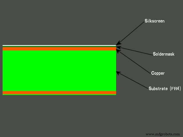
이를 스크린 인쇄라고도 하며 PCB 측면에서 기판에 잉크(주로 녹색)를 그림으로 추가하는 데 사용되는 인쇄 기술입니다.
보드에 문자, 숫자, 기호 및 이미지(전원 콘센트 및 콘센트, 잠재적인 마이크로칩 배치, 변압기 위치, 플러스+ 및 마이너스-)와 같은 것을 표시하는 데 사용됩니다. 일반적으로 한 가지 색상만 사용하며, 일반적으로 가시성이 상대적으로 낮습니다.
이것은 PCB의 두 번째 레이어입니다. 보드의 구리 흔적에 있는 폴리머의 유사 광택 마감 레이어입니다.
그 역할은 산화 및 먼지 또는 파편이 솔더 패드 사이에 모이는 것과 같은 환경 요인으로부터 보호하는 것입니다. 솔더 마스크는 또한 우리가 솔더 브리지라고 부르는 것을 방지하는 데 도움이 됩니다. 납땜 인두를 사용하는 동안 미끄러짐이 발생하여 두 도체가 접촉하여 납땜 브리지가 발생합니다.
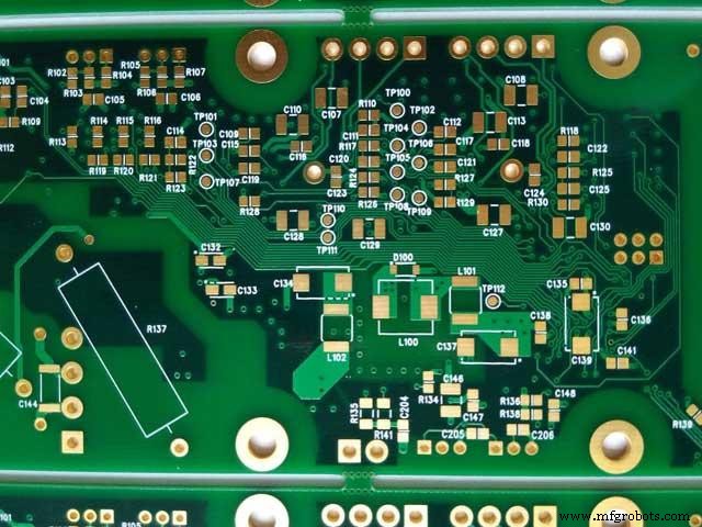
구리는 PCB에 탁월한 고성능을 제공합니다. 그것은 PCB 재료의 표면 거칠기와 구리가 유전체 재료와 결합될 때 제공합니다.
이 둘은 함께 작동하여 특히 RF 및 마이크로파 주파수에서 PCB에 탁월한 성능 출력을 제공합니다.
구리는 PCB의 신호 경로를 보여줍니다. 귀하가 보는 회로 패턴은 고품질의 구리만 고정밀도로 만들어집니다. PCB의 기판 재료와 잘 결합되면 생성할 수 있습니다.
구리의 열팽창 계수(CTE)는 약 17ppm/°C이며, 이는 전자 장치가 작동을 시작할 때 재료가 겪는 팽창 및 수축의 양입니다.
아래층의 기판인 보드 기판은 일반적으로 에폭시 수지와 강화재(유리 섬유, 때로는 직조 또는 부직포, 종이도 사용됨)로 주로 구성된 유전체 복합 재료입니다.
수지로는 필러형 세라믹이 사용되는 것으로 알려져 있다. 가장 일반적인 유형의 기질은 FR -4(FR은 난연제를 나타냄)입니다. FR-4 구리가 최고라고 말할 수 있는 이유는 유리섬유 기판 사이에서도 두각을 나타내는 뛰어난 전도성 때문입니다.
FR-4 구리의 또 다른 특징은 고강도, 유전 특성 및 겉보기 열 저항입니다. 구리와 기판의 용융은 PCB의 성능과 신뢰성에 가장 중요합니다.
앞서 언급했듯이 PCB의 두께와 무게를 항상 고려한 후에 사용해야 합니다.
예, 구리 PCB는 훨씬 더 많은 열 저항과 전기 전도성을 가질 수 있습니다. 슈퍼컴퓨터에서 비퍼용 PCB를 사용한다는 의미는 아닙니다. 그것은 낚시줄이나 미끼 없이 줄만 가지고 물고기를 잡으려는 것과 같습니다. 특정 실패.
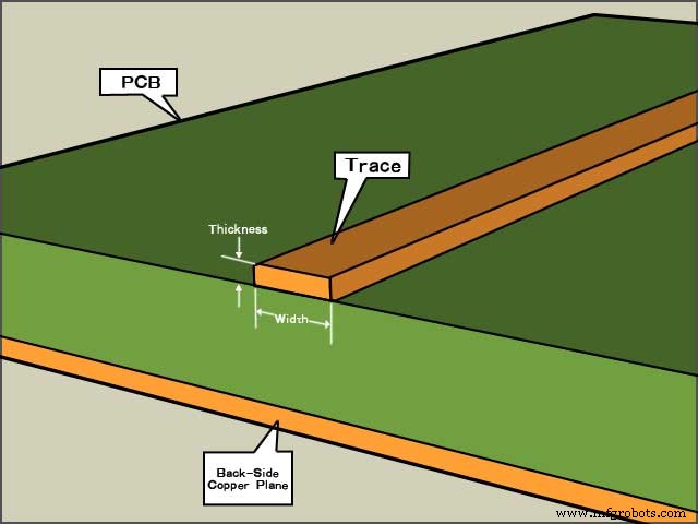
두께에 대한 표준 구리 측정 단위는 오즈입니다. (온스). 그러나 인치 단위로 측정할 수 있습니다. 대부분의 경우 사람들은 PCB와 관련하여 구리의 두께를 고려하지 않지만 1oz 구리를 평평하게 누르고 1평방피트 영역에 균일하게 펼친 후 전체 PCB의 두께를 고려합니다.
거의 모든 인쇄된 PCB는 1oz 구리 두께로 제작됩니다. PCB 제조와 관련하여 제조업체는 1온스를 가정합니다. 고객이 특정 사양을 제공하지 않는 한 설계를 인용하고 구성합니다.
고객은 설계에 1온스 이상의 추가 전류가 필요하고 전달할 수 있다고 결정했습니다. 그런 다음 구리 너비를 늘리거나 트레이스 너비를 늘리는 것이 더 좋습니다. 어떤 경우에는 완성된 구리가 1온스입니다.
일반적으로 2온스. 1온스 구리 두께는 의심할 여지 없이 가장 친숙하고 표준적인 구리 중량입니다. 종종 과도하지도 않고 너무 적지도 않은 지점에 도달하기 때문입니다. 구리 두께는 과도하고 비용이 많이 들지만 0.5 구리는 특히 더 높은 전류를 견디는 데 필요한 접지면에 적합하지 않을 수 있습니다.
따라서 1oz 구리 두께는 설계 및 재정적 요구 사항에 가장 적합한 옵션인 경우가 많습니다.
더 촘촘한 추적과 공간이 필요한 경우 일반적으로 해야 합니다. 무거운 구리가 필요한 레이어를 복제하고 구리를 두 개로 자르십시오. 8mil 라인과 4oz 구리가 필요하다고 가정하면 가장 좋은 옵션은 레이어를 복제하고 2oz를 사용하는 것입니다. 구리.
5온스 무게의 구리 추를 시작하기 위해. 또는 그 이상인 경우 두꺼운 구리 대신 레이어를 두 배로 늘리는 것이 좋습니다. 두꺼운 구리의 처리 복잡성을 고려할 때 두꺼운 구리를 사용하는 것보다 레이어를 추가하는 것이 저렴합니다.
다시 말해서 2층 6온스 구리판은 일반적으로 4층 3온스 구리판보다 가격이 비쌉니다.
대부분의 고객이 묻는 첫 번째 질문은 PCB 제조업체의 BAC-Final-Web-107Minimun 라인 너비 기능을 기반으로 합니다. 그러나 대부분의 경우 구리 무게가 답이 되는 경우는 드뭅니다.
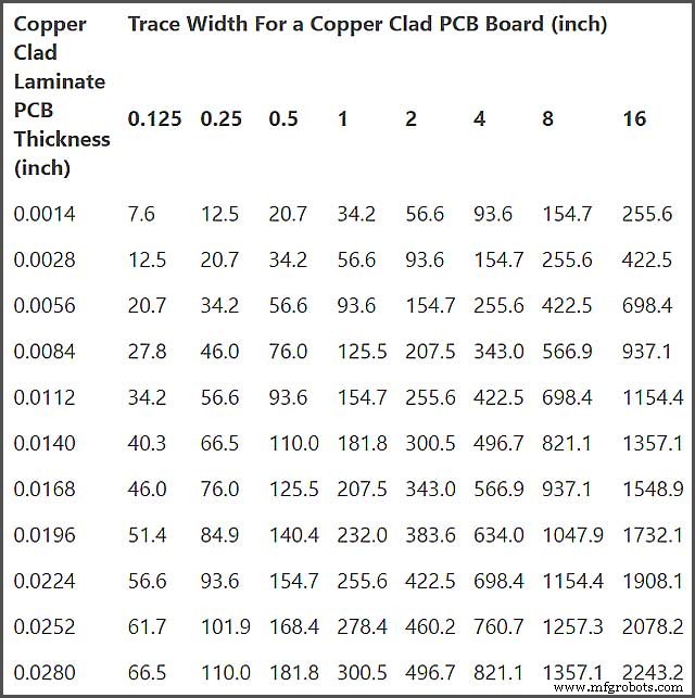
위의 표는 너비에 대한 구리 두께를 나타냅니다.
우리는 구리 PCB 두께의 중요성에 대해 이야기했습니다. 이제 구리 PCB의 무게가 두께만큼 중요한 이유를 자세히 살펴보겠습니다.
기본적으로 PCB의 무게는 항상 약 1.2oz입니다. 1 0z와 함께 구리. 구리 두께 및 도금된 스루 홀의 1mil 구리.
| 온스 | 그램 | 마이크론 |
| 1 | 300 | 35 |
| 2 | 600 | 70 |
| 3 | 900 | 105 |
물론 기본 범위는 0.5oz입니다. 3.0온스까지 동시에 도금된 구리의 범위는 0.7oz입니다. 2.0 온스. 구리의 무게가 높을수록 전기적 특성이 좋아지고 기판의 에칭 공정이 복잡해집니다.
1. 달성 가능한 추적 및 공간 너비 치수
2. 환형 링에 권장되는 최소 너비
3. 기본 구리는 라인에 필요한 감소량을 결정하므로 기본 구리가 많을수록 더 많은 라인 감소가 필요합니다.
1.내부 레이어에서 작동하지 않는 패드
2. 모서리에 허용 오차를 주어 단락을 방지할 수 있습니다.
3. 작은 구멍의 마이너스 공차를 목표로 합니다.
4. 항상 구리의 두께를 고려하십시오. 대부분의 경우 1온스에 불과합니다. 구리.
고급 PCB로 무거운 구리를 개발할 때 다층 PCB는 다양한 수준의 구리 2~5층 범위의 구리 레이어를 사용하여 생산됩니다. 유사한 구리 층을 사용하여 서로 연결된 것은 무엇입니까?
추가 구리 레벨은 보드의 기능을 향상시키고 추가 비아는 패드를 잘 부착된 상태로 유지하여 더 많은 전류 PCB를 전달하는 데 도움이 됩니다. 필요한 케이블을 제자리에 유지하여 볼트를 고정하는 거주지의 강도를 향상시키는 데 도움이 됩니다.
표면에서 최대 20마일까지 돌출된 무거운 구리를 교체하여 조립에 필요한 지원을 제공하는 새로운 저비용 제조도 개발되었습니다.
무거운 PCB에 사용되는 매립 기술은 기판 표면 위나 아래에 구리를 얼마든지 포함할 수 있습니다.
더 높은 전류의 PCB와 무거운 구리 기반 기판을 조립할 때 개발이 어려울 수 있지만 추가 시간과 노력이 필요하기 때문에 불가능한 것은 아닙니다.
이러한 기판을 개발하기 위해서는 열전달 형태의 열 전달을 관찰하여 기판을 설계하고 개발하는 엔지니어의 각별한 주의가 필요합니다.
무거운 구리가 있는 PCB는 더 나은 결과를 위해 충분히 높은 온도를 사용하여 납땜하고 올바르게 납땜해야 합니다. 더 높은 수준의 무연 온도를 사용하여 PCB를 제조하는 것이 좋습니다.
유지된 모든 열로 패드가 부착된 상태를 유지하는 데 도움이 되도록 적절하게 라미네이트할 것입니다.
웰PCB. 원스톱 서비스와 고품질의 제품을 제공하겠습니다. 필요한 서류를 보내주시면 바로 견적을 받아보실 수 있습니다! 우리는 무엇을 기다리고 있습니까? 우리는 10년 동안 PCB 제조를 시작했으며 PCB 제조 경험이 있는 사람들에게 중국에서 가장 중요한 옵션이 되었습니다. 이 제조에 관련된 사람들은 외국의 고객에게 필수 기능을 제공할 수 있습니다.
웰PCB. 우리는 비용 관련 문제로 인해 탄력을 얻은 중국에서 10년 동안 PCB를 제조했습니다. 원스톱 서비스와 고품질의 제품을 제공하겠습니다. 필요한 서류를 보내주시면 바로 견적을 받아보실 수 있습니다! 우리는 무엇을 기다리고 있습니까? 중국의 PCB 제조는 다른 지역 제조업체에 비해 비용이 저렴하기 때문입니다.
WellPCB는 중국에서 평판이 좋은 제조업체이기 때문에 서비스를 받을 수 있습니다. 그들은 소규모에서 대규모 WellPCB에 이르기까지 고객에게 서비스를 제공하고 있습니다. 원스톱 서비스와 고품질의 제품을 제공하겠습니다. 필요한 서류를 보내주시면 바로 견적을 받아보실 수 있습니다! 우리는 무엇을 기다리고 있습니까? 우리는 10년 간의 PCB 제조 경험이 있습니다.
주문하려면 웹사이트를 탐색하고 Gerber 파일을 통해 원하는 정보를 제출하는 것이 좋습니다.
추가 가격으로 맞춤형 PCB 어셈블리를 개발할 수 있는 탁월한 옵션을 고객에게 제공한 경험이 있으므로 PCB 제조에 필요한 사용자 정의 유형을 지정하는 것이 좋습니다.
회사는 귀하가 당사에 투자한 비용의 최대 가치를 얻을 수 있도록 가용한 자원을 보유하고 있습니다.
구리 피복 PCB에 대해 설명되지 않은 것은 무엇입니까? 당신은 엔지니어에게 물어보고 경제적으로 저렴함과 함께 부인할 수 없지만 동등하게 필수적인 이점에 대해 계속해서 그를 지켜봐야 합니다. 동박은 대부분의 엔지니어가 PCB를 만들 때 선택하는 기판입니다.
구리 피복 PCB는 생성되기 때문에 회로 위에 구성 요소를 쉽게 납땜할 수 있습니다. 코스 디자인에 탁월합니다.
동박 PCB는 소재의 경쟁력 있는 특성으로 인해 다른 기판에 비해 기판의 크기와 모양을 쉽게 사용자 정의할 수 있습니다. 사용 가능한 재료로 인해 다른 PCB 비용에 비해 전자 장치의 가격이 하락합니다.
구리 피복 PCB의 수많은 응용 프로그램 중 일부가 언급되었습니다. 구리 피복 PCB는 일반적으로 무기 제어 시스템, 레이더 시스템에 공급되는 전원, 고전력 평면 변압기의 1차 및 2차 권선, 배전 패널, 배터리 충전기 및 모니터링 시스템에 사용됩니다.
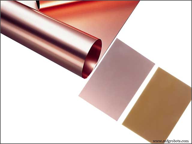
CCL(Copper Clad Laminate)로 약칭하며 목재 펄프지 또는 유리섬유를 수지에 담가 만든 모재와 보강재를 말합니다.
CCL은 다음과 같이 분류할 수 있습니다.
기계적 강성, 단열재, 두께 및 보강재 유형에 따라 다양한 분류 기준에 따라 분류됩니다.
Simple, an excellent CCL needs to meet specific requirements to be called EXCELLENT, which includes
do you like dents and scratches in your car? Guessing no, well same for CCL; a cut, gash, wrinkle, or pinholes can lead to low performance in the CCL and turn the PCB. So the smoother and cleaner the job, the better the performance.
Your CCL is a base material for the PCB; it needs to conform to the size requirement of the PCB.
this is the primary mission of the CCL which means it’s the primary mission of the PCB; specific details have to be paid to the Volume Resistance, Insulation Resistance, Dielectric constant, Arc resistance, and so on.
In physical performance, it’s always noteworthy to consider the bending strength, thermal stress, heat resistance, and punching quality.
The requirements needed to be met by the CCL are flammability, dimension stability.
The CCL should meet water absorption standards.
Within the CCL is what we call a prepreg, which is reinforced material; it is the reinforcement material used in a CCL. It is made of fiber and is referred to as the bonding sheet. It is mainly made of fiber cloth, epoxy resin, acetone, and many others.
Using quality prepreg results in high-quality CCLs, which enhances the quality of PCB. The quality of the prepreg material used depends on the resin content, resin fluidity, and dicyandiamide crystallization. Consequently, you should select resin based on the quality and the cost.
The cost should be related to the thickness of the fiber cloth. Thinner prepreg is recommended even though it might be a little bit costly.
To meet Restriction of Hazardous Substances Regulations, it is recommended that you look at the reliability and heat resistance of the CCls. The latest CCL has been enhanced by modifying them so that they:
Include Halogen-free CCL – refers to CCL with the content of bromine and chlorine controlled within 900ppm. Care should be taken so that the content does not exceed 1500ppm.
Lead-free CCL – refers to Copper laminate with surface mounting that has been carried out without applying lead-free solder. The epoxy resin may be used, but the RoHS regulations must be adhered to. Note that RoHS prohibits the use of substances such as PBDE and PBBD substances.
Resins used in CCls could be classified as:
If you are using fiber, the following quality aspects should be considered:
This is the used clad that is over the dielectric layer and substrate (resin composite material).
The copper acts as a composite insulator material while being a good conductor, also remember. You can have rigid or flexible base material. Still, the primary purpose of the copper laminate is to act as mechanical support for the pin, i.e., the firm base that holds the electronic component and joins them at the same time.
The most popular types of copper laminates used for PCB are:
This is a base material used for high-temperature PCB applications; it has an excellent glass transition (Tg =220 °C) that gives it an outstanding performance over high temperatures. It allows for soldering and desoldering of components, giving you more legroom for mistakes.
This base material is used in low-cost applications with the FR-2, CEM-1, or CEM-3 brand names. It is most widely used in single-layer PCB of small household gadgets and appliances. It is slightly brittle but hard to bend.
So far, it’s one of the most devise base materials with different applications just behind the FR -4; it is the preferred base material for multilayer PCBs; you find them in military, wireless, and communication systems.
This is a glass fiber base material that is durable, hard to bend, and cut with fire retardant qualities; it’s Tg =160°C. Because of all these qualities, various applications within single, double, and multilayer PCBs are used for power supply, mixed-signal and digital applications.
Other Copper Laminates used are Tetrafunctional epoxy, Thermount, and cyanate ester.
For electrically interconnecting the components, the laminates can be nickel, stainless steel, aluminum, and copper. However, the most widely used material for lamination purposes is copper. The aluminum found commercial applications recently and is appreciated in low-cost home appliances.
The conductive cladding layer is skinny and is over one or both sides of the resin composite material. The thickness of the cladding material is determined by how much material is deposited regarding weight.
It is a simple process but requires that you take some precautions. First, you need to turn the laminator on before feeding the board and the film in the machine. The side with the excess border should be provided into the laminator.
In most cases, you are required to put the board into the machine for the second time if you want to improve the quality of your clad board. It means that the board should be put back into the laminator immediately after it finishes the first run.
The same procedure should be used if you are working on a double-sided board.
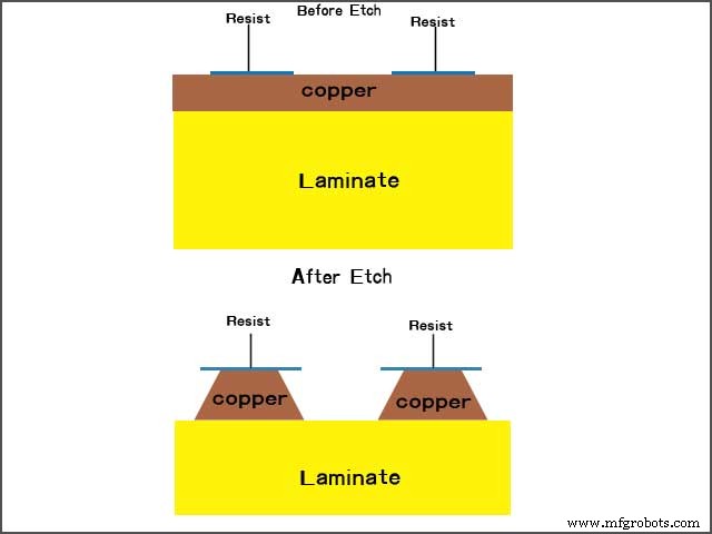
A keen eye is kept by designers when designing copper PCB; a designer must think in reverse. A board starts as solid copper; then, you remove the bits you don’t want.
It is faster to build, less expensive, and consuming when the copper is the same size as the board. Some techniques can make much difference from a frustrating experience to a smooth experience.
Maximizing copper is most common in two ways:
By specifying the specs of your PCBs (shape and size), this method is faster but sloppy as copper can be placed as an object, and these objects are checked for minor errors when assigned to a net. This method is mainly used for quick turns or prototype builds.
However, this method is more time-consuming than the manual process, but the pour method helps to maximize copper. Copper will be left behind by drawing a border around the board area and pouring the copper in, laying out the board, and going back and placing copper shapes to fill it.
What you need to know is that when the copper pour is used, you define your boundary and everything inside when the pour operation is performed while connected automatically.
This method usually favors a large area, several irregularly shaped objects, or unusual shapes. The pour operation automatically fills the unique body while additionally isolating other traces in the area.
Objects that the copper pour can automatically handle are Traces, nets, decals, and pads. When used right, you don’t need much; the copper pouring will make the right moves and connections; you can double-check using the continuity check tool.
Now we have talked about both the manual and automatic methods, and you probably think the manual process is the best, especially for the short time sprint. Still, in the long run, the intuitive approach can be better even though it is works upfront.
There are three situations when using a copper pour might be the better option for your design.
Manual – when you’re dealing with regular polygons, this method could be time-consuming and messy. A quick fix would be to drop overlapping shapes on top of each other to build your required profile.
It is quick, but it’s a short-term solution as eventually, you will need to do vertex editing to clean the design.
Automatic – The copper pouring method here is a “no-brainer” because we deal with complex shapes; this process is automatic. By defining the border and running copper, you eliminate the tedious job of re-editing later.
Manual – A plane is a large area of copper where all connections are one net. If you intend to build a board with separate planes while changing parts often, you often recommend route traces point to point.
Automatic – An excellent way to avoid several traces that all go to the same point is to use a copper pour method design on a plane for the ground. This will automatically connect all the connections on one network.
Manual – if you have a Hot board with much space, the best way to cool it down is to add a copper square to help conduct the heat away. Which may not always be the case?
Automatic – when you define the area around the critical parts of the board, prioritizing them, you can minimize the thermal stress. This method is used when importance is placed on maximizing the copper surface area.
Plating is very important to a PCB board. If all the traces on the external layers are not protected, the copper PCB will oxidize and deteriorate, making the board unstable. How do you know your copper has corroded? It will turn green. The two main reasons for plating are also called copper coating and surface finish:
1. To protect exposed copper circuitry
2. To provide a surface good enough for soldering when assembling components to the PCB.
You have various PCB copper plating options to choose from, and each carries its advantages and disadvantages. You can find them here.
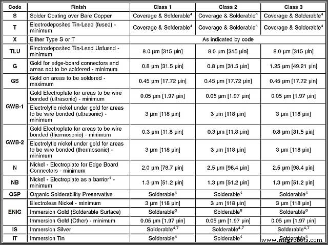
There are IPC standards for surface plating which is shown below:
Getting the best results is essential for you to clean your board using fine wool. You may also choose to use an abrasive pad before rinsing it with water. It helps to remove the dirt and any other contamination.
Alternatively, you may start by cleaning the dry board by exposing it to heat for about 5 minutes. This way, it ensures that the board is clean and ready for the film.
But I can answer you with one sentence “Copper PCB is the most reliable, effective PCB used across the most electronic device,” you don’t need to take my word for it. Just take a look at your phones.
And we at WellPCB are here to meet your needs at any time.
산업기술
2016년 4월 6일 인쇄 회로 기판은 재활용 조직에서 매우 중요한 제품으로 간주됩니다. 그 이유는 보드가 다양한 귀중한 재료로 설계되었기 때문입니다. 몇 가지 예에는 땜납, 금, 니켈, 주석 금속, 팔라듐 및 다양한 유형의 구리(산화물, 수산화물 및 황산염 용액)가 포함됩니다. 또한 강한 잉크 및 산과 같은 많은 PCB 액체는 환경 규정에 따라 위험한 것으로 간주됩니다. 따라서 인쇄 회로 기판을 적절히 재활용하는 것이 중요합니다. 제조 공정이 세부적인 것처럼 PCB 재활용 공정도 여러 단계로 구성됩니다. 하나의 포스트로 모
2017년 8월 31일 완벽하게 작동하는 인쇄 회로 기판(PCB)은 세심한 조립 프로세스의 결과입니다. 보드는 제조 과정에서 여러 단계를 거쳐야 합니다. 그들은 무엇인가? 계속 읽으십시오. 인쇄 회로 기판 조립과 관련된 단계는 무엇입니까? 인쇄 회로 기판 어셈블리(PCBA)와 관련된 여러 개별 단계가 있습니다. 다음은 다음과 같습니다. 1단계 – 솔더 페이스트 적용 이것은 PCB 어셈블리의 가장 첫 번째 단계입니다. 구성 요소를 계속 추가하기 전에 솔더 페이스트를 추가해야 합니다. 솔더를 적용할 회로 기판