이산화티타늄(TiO2 ) 나노 입자는 다양한 나노 입자 크기, 리프팅 속도, 전구체 농도 및 침지 수를 갖는 침지 코팅 기술을 통해 불소 도핑된 산화 주석(FTO)에 수정되었습니다. 변형된 FTO 전극과 평평한 FTO 전극 사이에 적절한 양의 겔 전해질을 끼워 가역적인 3상 광학 변환(투명, 거울 및 검정색)을 갖는 전착 기반 전기 변색 장치를 후속적으로 제작했습니다. 딥 코팅 공정 엔지니어링, TiO2의 형태적 특징 간의 상관관계 박막, 즉 두께 및 거칠기와 전기 변색 소자의 성능, 즉 광학 대비, 스위칭 시간 및 사이클링 안정성을 조사했습니다. 수정된 장치는 57%의 높은 광학 대비, 6초 및 20초의 짧은 착색/표백 전환 시간, 딥 코팅 공정 엔지니어링을 조정하여 27% 감소율의 1500 주기 후 우수한 사이클링 안정성을 나타냅니다. 이 연구의 결과는 만족스러운 성능을 가진 전기 변색 소자의 합리적인 설계를 위한 귀중한 지침을 제공할 것입니다.
<섹션 데이터-제목="배경">
배경
전기 변색 재료의 매력적인 특징은 전압이 가해지면 가역적이고 지속적인 방식으로 광학 특성을 변경할 수 있다는 것입니다. Deb[1]의 선구적인 작업 이후 다양한 전기 변색 재료가 개발되었으며, 이는 전이 금속 산화물[2], 프러시안 블루[3], 전도성 고분자[4], viologens[5]와 같은 여러 하위 집합으로 그룹화할 수 있습니다. , 전이 금속 이온 배위 화합물 [6], 하이브리드 전기 변색 재료 [7] 및 가역적 전착 기반 전기 변색 재료 [8, 9]. 광학 대비, 스위칭 시간, 착색 효율, 사이클링 안정성 및 광학 메모리 효과를 포함한 전기 변색 성능이 광범위하게 조사되어 스마트 윈도우, 눈부심 방지 백미러, 전기 변색 디스플레이, 전자 종이 및 군용 위장 [10,11,12,13,14,15,16,17,18,19]. 가역적 전착을 기반으로 하는 전기변색 소자는 샌드위치형 구조가 간단하고 제작이 쉽고 비용이 저렴하기 때문에 광 변조에 응용할 가능성이 있습니다. 이들의 광학적 특성은 인가된 전압 및 용해 하에서 투명 전도성 전극에 금속(구리(Cu), 비스무트(Bi), 플럼범(Pb), 니켈(Ni), 은(Ag) 등)을 증착하여 조작할 수 있습니다. 전압 제거 시 금속을 다시 전해질로 전환 [20,21,22,23,24,25,26]. 비스무트-구리(Bi/Cu) 전착 장치는 Bi와 Bi
3+
사이의 산화 환원에 의해 활성화되는 흑색과 투명 상태 사이의 신속하고 가역적인 전환으로 인해 정보 디스플레이에 널리 사용됩니다. [9, 23,24,25]. 유사하게, Ag 기반 전착 시스템[26,27,28,29]은 거울 상태를 실현하는 능력을 위해 전기 변색 장치를 제조하기 위해 개발되었습니다.
일반적으로 적절한 전극 표면 수정은 수정된 전극 표면의 빛의 흡수 및/또는 다중 산란으로 인해 전착 기반 전기 변색 장치의 가역적 및 다중 색상 상태를 유발할 수 있습니다[30,31,32,33]. 스퍼터링[34], 진공 증발[35], 화학 기상 증착[36], 열수[37], 전착[38] 및 졸-겔[39, 40]을 포함한 다양한 기술이 전기 변색 박막을 제조하는 데 사용되었습니다. . 다양한 기술 중에서 졸-겔 접근법은 비용이 저렴하고 대면적 준비가 용이하며 취급이 용이한 장점이 있으며 그 중 스핀 코팅 및 딥 코팅 기술이 널리 사용됩니다. 스핀 코팅과 비교하여 딥 코팅 기술은 제어 가능성이 높고 대규모 준비에 더 적합하기 때문에 선호됩니다[24]. 또한 Deepa et al. [24] 또한 삼산화 텅스텐을 기반으로 하는 침지 코팅된 전기 변색 장치(WO3 ) 박막은 향상된 투과 변조, 착색 효율, 스위칭 속도, 착색/표백 주기와 같은 스핀 코팅된 장치에 비해 우수한 성능을 보였다. 그러나 침지 코팅 기술은 전착 기반 Ag/Cu 전기 변색 소자의 제조에 아직 적용되지 않았습니다.
기본적으로 전기 변색 재료의 전기 변색 성능(즉, 광학 대비, 스위칭 시간, 착색 효율, 사이클링 안정성 및 광학 메모리 효과)은 기본적으로 구조, 표면 형태 및 구성 특성에 따라 다릅니다[41]. 따라서 전기 변색 재료의 특성 향상을 위해 준비 매개 변수를 자세히 검사하는 것이 매우 필요합니다. Deepa et al. [42] 조작된 WO3 딥 코팅 기술을 통한 필름, 및 WO3 어닐링으로 얻은 필름이 제시되었습니다. 투명 상태와 청색 상태 사이의 더 빠른 스위칭 속도, 리튬 삽입에 대한 더 큰 전류 밀도, 리튬에 대한 더 높은 확산 계수 및 우수한 사이클링 안정성은 습도 변화가 75% RH에서 제조된 필름에 의해 얻어집니다. 전기 변색 재료의 구조 및 전기 변색 특성. Sun과 그의 동료들[43]은 WO3를 준비했습니다. 스핀 코팅 방법과 결합된 졸-겔 경로에 의한 박막. WO3의 미세 구조 및 광학 특성에 대한 어닐링 온도의 영향 필름이 조사되었고 더 낮은 어닐링 온도에서 가시 범위에서 더 높은 투과율 변조가 얻어졌습니다. 전구체 졸의 유기 부분의 유형 및 함량, 필름 제조 방법(스핀 또는 딥 코팅)이 필름 특성에 미치는 영향도 광범위하게 조사되어[43, 44], 전기 변색 성능 및 전기 변색 박막의 제조 매개변수. Araki et al. 스핀 코팅을 통해 수정된 ITO(Indium Tin Oxide) 전극에 Ag를 증착하고 가역적인 흑색 및 거울 상태를 얻었다. Tsuboi와 그의 동료[42, 44]는 다양한 전압에서 Ag 입자의 성장을 제어하여 여러 색상 상태에 대한 추가 추적을 수행했으며, 이는 나노 입자의 크기와 모양을 조작하면 극적인 변화를 초래할 수 있음을 나타냅니다. 색상으로. 우리의 이전 연구[33]에서 우리는 전도성 TiO2를 사용하여 가역적인 3상태 광학 변환(투명, 흑색 및 거울 상태)을 갖는 전착 기반 Ag/Cu 전기 변색 소자를 제작했습니다. 스핀 코팅 기술을 통해 제작된 나노입자 변형된 불소 도핑된 산화주석(FTO) 전극. 우리는 또한 TiO2의 표면 구조를 조작하여 다양한 상태에서 장치의 광학적 특성을 효과적으로 제어할 수 있음을 입증했습니다. -수정된 FTO 전극. 그러나 다중 상태 전기 변색 소자에 대한 전극 표면 개질 효과에 대한 면밀한 조사는 거의 보고되지 않았습니다. 따라서 제조 매개변수를 통해 전착 기반 전기 변색 소자 특성에 대한 철저한 조사가 중요합니다.
이 연구에서 TiO2 나노 입자는 딥 코팅 기술을 통해 FTO에 수정 된 다음 수정 된 FTO 전극과 평평한 FTO 전극 사이에 적절한 양의 겔 전해질을 샌드위치하여 가역적 인 3 상태 광학 변환을 갖는 전착 기반 전기 변색 장치를 제작했습니다. 딥 코팅 기술의 높은 제어 가능성을 위해 전극 표면 수정을 조작하여 장치의 광학 성능을 조정할 수 있습니다. 나노 입자 크기는 조작될 수 있고 제조된 장치의 성능을 다르게 만들 수 있는 중요한 매개변수입니다. 따라서 나노 입자 크기는 TiO2의 미세 구조에 미치는 영향을 조사하기 위해 조정됩니다. 박막 및 제조된 장치의 성능. 나노 입자 크기를 제외하고 리프팅 속도, 전구체 농도 및 침지 횟수는 딥 코팅 공정의 주요 매개 변수입니다. 이때, TiO2의 미세구조에 미치는 영향을 알아보기 위해 리프팅 속도, 전구체 농도 및 침지 횟수도 변화시켰다. 박막뿐만 아니라 전기 변색 장치의 성능, 즉 투과율/반사율, 광학 대비, 스위칭 시간 및 사이클링 안정성. 이 연구의 결과는 만족스러운 성능을 가진 전기 변색 소자의 합리적인 설계를 위한 귀중한 지침을 제공할 것입니다.
방법
자료
크기가 25 × 30 mm, 두께가 2.2 mm, 면저항이 10 Ω sq
−1
인 FTO 투명 전도성 유리 무한 격자 태양 에너지 기술 유한 회사에서 구입 한 전극으로 사용되었습니다. 균일 한 TiO2 평균 직경이 5~10, 40 및 100 nm인 나노 입자(Aladdin Co. Ltd.)를 사용하여 FTO 전극을 수정했습니다. 디메틸설폭사이드(DMSO, ≥99.8%, J&K Chemical Co. Ltd.), 테트라-n을 포함한 전해질 화합물 -부틸암모늄브로마이드(TBABr, ≥99%, J&K Chemical Co. Ltd.), 질산은(AgNO3 , ≥99.8%, Guangdong Guanghua Sci-Tech Co. Ltd.), 염화구리(CuCl2 , ≥99.0%, KeLong Chemical Co. Ltd.), 폴리(비닐 부티랄)(PVB, Sekisui Chemical Co. Ltd.), 에틸 셀룰로오스(≥99.5%, Hanzhou Lanbo Industrial Co. Ltd.), 라우르산(≥99.8 %, KeLong Chemical Co. Ltd.), terpineol(≥98.0%, KeLong Chemical Co. Ltd.) 및 에틸 알코올(≥99.7%, KeLong Chemical Co. Ltd.)은 상업적 출처에서 얻었습니다. 모든 용매 및 화학 물질은 시약 품질이었고 추가 정제 없이 사용되었습니다. 두께 0.5mm의 테프론 시트(Aladdin Co. Ltd.)를 20 × 20mm 구멍으로 25 × 25mm로 절단하였다. FTO 유리 전극과 테프론 시트는 사용 전에 에탄올과 탈이온수로 여러 번 세척되었습니다.
TiO의 준비2 나노입자 분산 및 겔 전해질
TiO2를 준비하려면 나노입자 분산, TiO2 라우르산(계면활성제, 0.25g)과 에틸셀룰로오스(접착제, 0.75g)가 포함된 나노입자(원료, 2.5g)를 볼밀 용기에 먼저 넣고 테르피네올(접착제, 16mL) 및 에틸알코올( 밀링 직전에 용매, 10mL). TiO2 50분 밀링 후 나노 입자 슬러리를 얻은 후 에틸 알코올로 슬러리를 희석했습니다. 겔 전해질을 제조하기 위해 TBABr(806mg, 2.5mmol), 질산은(85mg, 0.5mmol) 및 염화구리(13mg, 0.1mmol)를 DMSO 10mL에 용해시킨 다음 PVB( 1.32g, 10wt%). 마지막으로 혼합 용액을 암실에 24~48시간 동안 두어 겔 전해질을 얻었다.
FTO 전극 수정 및 전기 변색 장치 제작
딥 코팅 기술을 사용하여 FTO 투명 전도성 전극을 수정했으며 일반적인 프로세스는 다음과 같습니다. 희석제로 에틸 알코올(10, 15 또는 20mL)을 TiO2에 첨가 나노입자 분산액(5mL), 30분 동안 초음파 혼합. 그 후, 전면과 후면 전체에 Tap을 붙인 FTO 전극을 딥 코터에 고정하고, 앞서 언급한 분산액에 6000μm/s의 속도로 침지하고, 1000, 2000, 3000μm/s의 속도로 들어 올렸다. , 각각. TiO2 나노입자로 변형된 FTO 전도성 전극은 500°C에서 30분 동안 준비된 샘플을 소결하여 얻었습니다. 비교를 위해 TiO2 다양한 크기(5~10, 40, 100nm)의 나노입자가 사용되었으며, 리프팅 속도(1000, 2000 및 3000μm/s), 전구체 농도(TiO의 비율)를 포함한 딥 코팅의 다양한 매개변수가 사용되었습니다. 2 본 연구에서는 나노입자 분산액과 에틸알코올 1:2, 1:3, 1:4), 침지수(1, 3, 5)를 사용하였다. 특히 TiO2의 영향을 조사하기 위해 전기 변색 소자의 성능에 대한 나노 입자 크기, TiO2 5~10, 40, 100nm 크기의 나노입자를 리프팅 속도를 3000μm/s, 전구체 농도를 1:2, 침지 횟수를 1로 고정하여 사용하였다. 리프팅 효과를 알아보기 위해 전기 변색 장치의 성능에 대한 속도, 1000, 2000 및 3000μm/s의 리프팅 속도는 TiO2를 고정하여 사용했습니다. 5~10 nm의 나노 입자 크기, 전구체 농도 1:2, 침지 수 1. 전기 변색 소자의 성능에 대한 전구체 농도의 영향을 조사하기 위해 TiO2의 비율 TiO2를 고정하여 나노입자 분산액과 1:2, 1:3, 1:4의 에틸알코올을 사용 5~10nm의 나노 입자 크기, 3000μm/s의 리프팅 속도, 1의 침지 횟수. 전기 변색 소자의 성능에 대한 침지 횟수의 영향을 조사하기 위해 침지 횟수 1, 3, 5 TiO2를 고정하여 사용 5~10nm의 나노 입자 크기, 3000μm/s의 리프팅 속도, 1:2의 전구체 농도. 전착 기반 전기 변색 소자를 조립하기 위해 DMSO 기반 겔 전해질을 20mm × 20mm의 밀폐된 정사각형 공간에 담고 0.5mm 두께의 테프론 시트 내부를 절단하고 두 개의 FTO 전극 사이에 테프론 시트를 끼워 밀봉했습니다( 그 중 하나는 TiO2로 수정되었습니다. 나노 입자).
특성화
전계 방출 주사 전자 현미경(FESEM, S-3400, Hitachi)을 사용하여 TiO2의 형태를 관찰했습니다. 나노입자로 변형된 FTO 전극. TiO2의 거칠기 나노입자로 변형된 FTO 전극은 원자간력현미경(AFM, Multimode V, Veeco)을 사용하여 특성화하였다. 전기화학적 워크스테이션(CHI660D, CHI)을 이용하여 전기변색 소자에 변환 전압을 인가하고 UV-Vis 분광광도계(Cary 5000, Agilent)를 이용하여 투과율 및 반사율 스펙트럼을 측정하였다. 광학적 대비, 스위칭 시간 및 사이클링 안정성을 포함한 모든 전기 변색 특성은 음극과 양극이 평평한 FTO 전극과 TiO2에 연결된 2전극 모드를 사용하여 얻어졌습니다. 나노입자로 변형된 FTO 전극. 측정 중 전기 변색 소자의 상대 전극은 평평한 FTO 전극이었고 작업 전극은 TiO2였습니다. 나노입자로 변형된 FTO 전극. 적절한 전압을 인가함으로써, 침지 코팅된 전기 변색 소자는 투명, 거울 및 흑색을 포함하여 3가지 가역적 광학 상태를 나타냈다.
결과 및 토론
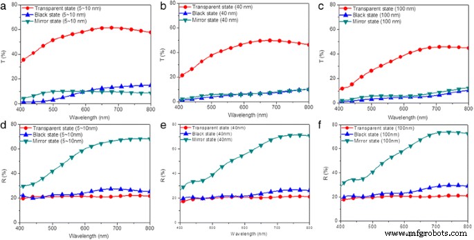
거울, 흑색 및 투명 상태 사이의 가역적인 3상 광학 변환은 전착 기반 전기 변색 소자에 적절한 전압을 교대로 인가/제거함으로써 달성될 수 있다. 블랙 및 미러 상태는 거친 TiO2에 증착된 Ag에 대해 트리거됩니다. 나노입자로 변형된 FTO 전극과 평면 전극에 각각. 따라서 수정된 소자의 흑색 상태는 표면 형태학적 구조에 의해 크게 영향을 받을 수 있습니다. TiO2의 표면 형태학적 구조의 영향을 조사하기 위해 수정된 장치의 성능에 대한 박막, TiO2를 포함하는 세 가지 전구체 용액 다양한 크기(5~10, 40, 100nm)의 나노 입자를 볼 밀링으로 준비했습니다. 그 후, 딥 코팅 기술을 통해 FTO 전극 표면에 전구체 용액을 코팅하고, 소결 처리하고, 변형된 FTO 전극과 평평한 FTO 전극 사이에 적절한 양의 겔 전해질을 끼워 변형된 소자를 얻었다. 먼저 투명, 거울, 흑색 상태의 3가지 변형 소자의 광투과율 및 반사율 스펙트럼을 400~800nm의 스펙트럼 영역에서 측정했습니다. 투과율 측정을 위해 평평한 FTO 전극과 TiO2에 전원의 음극과 양극을 연결하였다. nanoparticle-modified FTO 전극은 각각 +2.5V의 미러 상태와 20초 후 -2.5V의 블랙 상태를 나타냅니다. 반사율 측정을 위해 동일한 전압을 90초 동안 적용했습니다. 투명 상태에서 TiO2로 제조된 수정된 장치에 대해 61, 50 및 46%의 투과율이 관찰됩니다. 각각 5~10, 40 및 100nm의 나노 입자(그림 1a-c). 흑색 상태에서 TiO2로 준비된 수정된 장치 5~10nm의 나노 입자는 최대 투과율이 15%이고 TiO2의 크기가 증가하면 10%로 감소합니다. 나노 입자를 100nm로 변환합니다(그림 1a-c). 미러 상태에서 TiO2로 준비된 수정된 장치 5~10nm의 나노 입자는 40 및 100nm의 나노 입자와 유사한 투과율을 나타냅니다(그림 1a-c). 광학 대비는 일반적으로 착색과 표백 과정 사이의 전기 변색 장치에 대한 투과율, 반사율 또는 흡광도의 최대 차이로 정의됩니다. 투명 상태와 흑색 상태 사이의 장치에 대한 투과율 차이를 계산하여 48, 42 및 39%의 광학 대비를 얻습니다. TiO2 증가에 따른 광학 대비 감소 나노 입자 크기는 대부분 투명 상태에서 장치의 투과율 감소에 기인합니다. 5~10nm TiO2로 준비된 수정된 장치의 반사율 피크 나노 입자는 40 및 100nm TiO2로 준비한 것과 다릅니다. 각각 700, 750 및 750 nm에서 피크 위치를 갖는 나노 입자(그림 1d-f). 기본적으로 굴절률은 일반적으로 재료, 구조(즉, 멤브레인의 수와 배열), 두께 및 멤브레인의 계면 형태/구조에 의해 결정됩니다. 따라서 거울 상태에서 변형된 전착 기반 전기 변색 소자의 파장 의존적 반사 스펙트럼에서 피크 이동의 이유는 다양한 TiO2의 결합된 효과일 수 있습니다. 나노입자 크기, TiO2 박막 두께, TiO2 박막 표면 거칠기 [45,46,47]. 또한 거울 상태의 수정된 장치에 대해 70% 이상의 반사율이 관찰되었으며 검은색 및 거울 상태의 세 개 수정된 장치에 대해 20%의 낮은 반사율이 관찰되었습니다(그림 1d–f). 위의 값은 도달할 수 있는 가장 어두운 상태에 해당하지 않습니다. 전술한 결과는 TiO2의 크기에 따라 전착 기반 소자의 광투과율, 광반사율 및 광명암비가 변경될 수 있음을 시사한다. 투명전극에 증착된 나노입자.
<사진>
(Color online) 투명(red)의 전착 기반 전기변색 소자의 광학적 특성 ), 검정(파란색 ) 및 미러 상태(녹색 ). a로 준비된 수정된 기기의 투과 스펙트럼 5~10, b 40 및 c 각각 100nm입니다. d로 준비된 수정된 장치의 반사 스펙트럼 5~10, e 40 및 f 각각 100nm
침지 코팅된 TiO2의 구조적 특징 다양한 나노 입자 크기를 가진 박막을 조사했습니다. 소결된 침지 코팅된 TiO2에 대한 X선 회절(XRD) 패턴 필름, 준비된 상태로 딥 코팅된 TiO2 필름, 신선한 TiO2 추가 처리하지 않은 나노 입자 및 대머리 FTO 투명 전도성 전극은 2θ에 기록됩니다. 범위는 20° ~ 80°입니다[33, 48]. 추가 파일 1에 제시된 바와 같이:그림 S1a, 준비된 TiO2의 회절 피크 필름, 소결 TiO2 필름 및 신선한 5~10nm TiO2 추가 처리가 없는 나노 입자는 동일한 위치에서 발생하고 TiO2의 아나타제 구조 형태와 매우 잘 일치합니다. (TiO2 아나타제, JCPDS 21-1217). 이 값은 문헌 데이터[48]와 잘 일치하며, 확장된 분산 피크는 anatase 상의 결정 평면(101), (004), (200), (105), (211) 및 (204)에 상응하여 나타납니다. . 52° 및 62°에서 관찰된 추가 피크는 FTO 전극 표면에서 나오며, 이는 산화주석(SnO2)의 구조적 형태와 잘 일치합니다. , JCPDS 46-1088) [33, 49]. 유사한 아나타제 구조 형태가 40 및 100nm TiO2에서도 관찰됩니다. 소결 전후의 나노입자 수정 FTO 전극(추가 파일 1:그림 S1b 및 S1c). 침지 코팅된 TiO2 박막은 새로운 TiO2와 동일한 구조적 형태를 유지합니다. 코팅된 TiO2의 구조적 특징을 나타내는 FTO 전극을 수정하기 위한 전체 제조 절차에 걸쳐 나노 입자 박막은 딥 코팅 방법의 영향을 받지 않을 것이며 유사한 결과가 이전 보고서에서도 제시되었습니다[33].
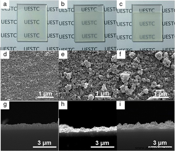
둘째, 3개의 침지 코팅된 TiO2의 형태학적 특징 박막을 조사했다. 침지 코팅된 TiO2의 사진, 평면 및 단면 SEM 이미지 Ag 증착 전 박막이 그림 2에 제공되었습니다. TiO2로 증착된 FTO 전극 나노 입자는 TiO2의 크기를 증가시킨 후 다른 투명도를 나타내며 점차적으로 흐려집니다. 나노 입자(그림 2a-c). TiO2로 제조된 박막 5~10nm의 나노입자는 입자 사이의 경계가 뚜렷하고 기공과 입자의 균일한 분포를 보여 균일하고 미세한 TiO2를 나타냅니다. 얻어진 박막(그림 2d). TiO2의 크기를 늘린 후 나노입자, 증착된 TiO2의 표면 그러나 박막은 거칠고 불균일해진다(그림 2e, f). TiO2의 이 불균일한 분포 나노 입자는 주로 딥 코팅 및 소결 과정에서 에틸 알코올의 점진적인 분산 감소와 덩어리로 인해 발생합니다. 점차 흐려지고 거친 TiO2 나노 입자의 크기가 증가하는 박막은 그림 1a와 같이 변형된 장치에 대한 감소된 투과율 스펙트럼을 보여줍니다. 일반적으로 3개의 TiO2의 두께 증가 박막은 단면 SEM 이미지를 통해 측정되며 두께는 TiO2입니다. 5~10, 40 및 100nm TiO2로 준비된 FTO 전극용 320, 409, 612nm의 박막 나노입자가 각각 관찰되었다. Dip-coating 과정에서 용매 증발 과정에서 입자 중력, 양력, 모세관력의 균형을 통해 연속적인 박막을 얻을 수 있습니다. 다양한 입자 중력과 모세관력으로 인한 다른 균형력은 나노입자 크기에 따라 예상되며, 이는 두께와 거칠기를 다르게 합니다. 그림 1a, b와 같이 TiO2를 증가시킨 후 투명 상태에서 수정된 소자의 투과율, 반사율, 광학적 대비가 변화함 나노 입자 크기. 따라서 확대된 TiO2에 대해 투명 상태에서 변형된 전기 변색 소자의 광 투과율이 낮아짐을 알 수 있습니다. 나노입자 크기는 주로 침지 코팅된 TiO2의 두께 증가로 설명할 수 있습니다. 박막.
<그림>
(컬러 온라인) TiO2 사진 a의 나노입자 크기로 제조된 박막 5~10, b 40 및 c 각각 100nm입니다. TiO2의 면내 SEM 이미지 d의 나노입자 크기로 제조된 박막 5~10, e 40 및 f 각각 100nm입니다. TiO2의 단면 SEM 이미지 g의 나노입자 크기로 제조된 박막 5~10, h 40 및 i 각각 100nm
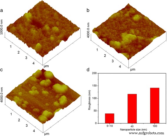
3개의 침지 코팅된 TiO2의 거칠기 박막은 그림 3a-c와 같이 원자간력현미경(AFM)을 사용하여 추가로 측정되었습니다. 침지 코팅된 TiO2의 거칠기 TiO2의 경우 거칠기가 39, 117 및 142nm인 나노입자 크기의 함수로서의 박막이 그림 3d에 표시되었습니다. 5~10, 40 및 100nm TiO2로 준비된 박막 각각 측정된 나노 입자. 더 큰 TiO2에 대해 더 많은 응집과 더 낮은 분산의 결과로 거칠기의 증가가 관찰됩니다. 나노 입자. 기본적으로 투과율 및 관련 반사율은 장치에 입사하는 파동의 거동을 설명하는 데 사용됩니다. 필수 지표인 굴절률 인자는 재료, 구조(즉, 멤브레인의 수와 배열), 두께 및 멤브레인의 계면 형태/구조에 의해 결정됩니다. TiO2의 크기가 다른 수정된 전착 기반 전기 변색 장치의 광학 특성을 조사할 때 앞서 언급한 모든 요소를 고려해야 합니다. 나노 입자. 수정된 장치의 검은색 상태를 트리거한 후 모든 FTO 표면이 어두운 검은색으로 변하여 Ag 층이 FTO 전극의 표면 형태를 크게 수정함을 나타냅니다(추가 파일 1:그림 S2a, S2b 및 S2c). 증착된 Ag 층이 있는 수정된 장치의 모든 FTO 표면은 대머리 TiO로 코팅된 것보다 더 부드러워집니다2 박막(추가 파일 1:그림 S2d, S2e 및 S2f). 침지 코팅된 TiO2의 단면 SEM 이미지 박막(추가 파일 1:그림 S2g, S2h 및 S2i)도 세 가지 수정된 장치 모두에 대해 두껍고 컴팩트한 Ag 증착 층을 나타냅니다. 그림 1과 같이 Ag 증착 후 투과율 및 반사율 스펙트럼이 변경되고 장치가 흑색 상태로 변환되어 투과율 및 반사율에 대한 두께 및 거칠기의 강한 영향을 나타냅니다. 추가 증착된 Ag 층, 변경된 두께 및 상단 층의 계면 형태를 포함하여 변경된 멤브레인 구조의 결합된 효과를 고려해야 합니다.
<그림>
(Color online) TiO2의 AFM 이미지 a의 나노입자 크기로 제조된 박막 5~10, b 40 및 c 100nm 및 d TiO2의 거칠기 TiO2의 함수로서의 박막 나노입자 크기
세 번째로, 700nm에서 3개의 수정된 장치의 시간 의존적 투과율 변화는 4개의 연속적인 착색/표백 주기 및 100mV/s의 스위프 속도로 2전극 CV(Cyclic voltammogram) 테스트 중에 측정되었습니다. 투과율 측정을 위해 TiO2에 +2.5V와 -2.5V의 전압을 교대로 인가했습니다. -20초 동안 수정된 FTO 전극. 그림 4는 TiO2로 준비된 수정된 기기의 시간 경과에 따른 투과율 변화를 보여줍니다. 다양한 크기의 나노 입자. 5~10, 40, 100nm TiO2로 제작된 변형 소자의 초기 투과율 나노 입자는 표백 시 61, 50, 46%에 도달하고 착색 시 각각 34, 25, 18%로 떨어집니다. 기본적으로 착색 과정은 장치가 투명 상태에서 거울/검정 상태로 변하는 것을 의미하고 표백 과정은 장치가 거울/검정 상태에서 투명 상태로 반대로 변하는 것을 의미합니다. 착색/표백 전환 시간은 착색 및 표백 과정에서 최대 변조의 90%에 도달하는 데 필요한 시간으로 표현됩니다. TiO2로 수정된 장치에 대해 다른 전환 시간이 측정되었습니다. 다양한 크기의 나노 입자, 5~10nm TiO2로 준비된 수정된 장치 착색과 표백 과정 사이에 가장 짧은 전환 시간(착색의 경우 6초, 표백의 경우 20초)을 나타내는 나노 입자입니다. 나노입자 크기의 증가에 따른 스위칭 시간 증가는 FTO 전극이 더 얇고 매끄러운 TiO2로 개질되었음을 보여줍니다. 박막은 착색/표백 전환 시간을 단축하는 데 기여합니다. 또한 표백 과정은 모든 소자에 대한 착색 과정보다 느립니다. 이는 전기 변색 소자에 대한 대부분의 기사에서 확인할 수 있습니다. 더욱이, 수정된 소자가 투명에서 거울 상태로 변하는 시간은 소자가 투명에서 흑색 상태로 변하는 시간보다 짧아서 거친 TiO2 FTO 전극에 증착된 박막은 스위칭 시간에 영향을 미칩니다. 또한, 다공성 전이금속 산화물 박막 공정의 최근 발전은 특성이 향상된 전기변색 소자의 구성에 새로운 기회를 제공했습니다. 예를 들어, Zhang et.al은 전착된 주기적인 그릇 모양의 거대 다공성 WO3 자체 조립 단층 폴리스티렌(PS) 구를 템플릿으로 사용하여 ITO 유리에 전착된 어레이 필름은 PS 템플릿 없이 준비된 조밀한 필름과 비교할 때 3.6초의 훨씬 빠른 착색 시간을 나타냅니다[50]. Yang과 동료들은 정렬된 거대다공성 WO3의 제작을 보고했습니다. 템플릿 보조 졸-겔 방법을 통해 제조된 박막. 착색 시간은 5.19초로 고밀도 필름보다 현저히 짧은 6.9초[51]로 얻어진다. They also demonstrated that the electrochromic response time is actually limited by two factors:the ion diffusion coefficient and the length of diffusion path, with the former one depends on the chemical structure, while the latter depends on the microstructure.
(Color online) Transmittance variations at 700 nm obtained during two-electrode CV tests for devices modified with TiO2 nanoparticle sizes of 5~10 (red ), 40 (blue ), and 100 nm (green ), respectively
The coloration efficiency, CE (cm
2
/C ), is one of the best parameters often used to evaluate an electrochromic device. CE is defined as the change in the optical density (ΔOD) per unit of injected/extracted charge (Q ) at a certain wavelength [17], which can be calculated from the following formula
where ΔOD is the change in the optical density, Q (C /cm) is the charge injected per unit electrode area of the thin film, and Tb and Tc are the transmittance in the bleached and the colored states, respectively. The coloration efficiency of the modified devices prepared with 5~10, 40, and 100 nm TiO2 nanoparticles were listed in Additional file 1:Table S1. CE of 27.0, 20.7, and 16.9 cm
2
/C at 700 nm were obtained for modified devices prepared with 5~10, 40, and 100 nm TiO2 nanoparticles, respectively. The decreased CE value indicates that the modified devices prepared with 5~10 nm exhibits a large optical modulation with a small intercalation charge density. This decreased CE of the electrochromic devices may be due to the increased TiO2 nanoparticle size and TiO2 thin film thickness and roughness, as demonstrated by previous reports [52,53,54].
Generally, device failure occurs after repeatedly switching an electrochromic device between its coloration and bleached states for hundreds or thousands of times. This attributes to the combined effect of various side reactions including transparent electrode failure, electrolyte depravation, and active layer decay. Thus, cycling stability of the modified devices is further investigated by repeatedly applying sequential voltages. As shown in Fig. 5, transmittance variation of the three modified devices at 700 nm was measured by applying voltages of −2.5 V. Every 500 cycles was taken as a measurement node to measure the transmittance deviation of modified devices over time. The measured transmittance of the three devices are all below 1% and maintain fairly stable after the devices transferred into black state and the voltage removed for the first cycle. The transmittance of the modified devices in transparent states gradually decrease and increase for coloration states with the time and the cycle numbers, indicating more cycles lead to poorer stability. The optical contrast of the modified device prepared with 5–10 nm TiO2 nanoparticles decreases from 48 to 35% after 1500 cycles (Fig. 5a). As shown in Fig. 5b, c, the optical contrasts of modified devices prepared with 40 and 100 nm TiO2 nanoparticles decrease to 23 and 16%, respectively, indicating that the cycling stability can be improved by decreasing the size of TiO2 nanoparticles. To investigate the trace of Ag dissolution in the electrolyte for the sample with less stability, the morphological features of the dip-coated TiO2 thin film after manifold cycles were investigated. The SEM of dip-coated 100 nm TiO2 thin film after 1500 cycles was presented in Additional file 1:Figure S3. As shown in Additional file 1:Figure S3, uneven electrolyte agglomeration is observed for the dip-coated TiO2 thin film in our work, which is similar to that of the previous reports [55, 56]. Moreover, extra Ag was detected via energy-dispersive spectrometer (EDS) in the dip-coated TiO2 thin film after the transformation of modified device to the transparent state, with the results listed in the Additional file 1:Table S2. We supposed that the ability to achieve complete reversibility is deteriorated due to the gradual deposition of Ag onto bumps of TiO2 thin films and inability to dissolve Ag back into electrolyte immediately during the continuous cycling between the coloration and bleaching states. Thus, the improved cycling stability might be owed to the decreased surface roughness of TiO2 thin film, which is conducive to the quick dissolution of Ag back into electrolyte during the switching between the coloration and bleaching states, and the surface roughness of TiO2 thin film is strongly influenced by the TiO2 nanoparticle size. Therefore, both the particle size itself and the surface roughness are related to the improved cycling stability.
(Color online) Transmittance variation for dip-coated devices prepared with TiO2 nanoparticles of a 5–10, b 40, and c 100 nm, respectively, in transparent (black ) and black (red ) states at 700 nm after applying a sequence of voltages in the following order:−2.5 V (10 s), 0.5 V (30 s), 2.5 V (10 s), 0.5 V and (20 s), with each of the 500 cycles taken as a measurement node
In summary, improved optical contrast, switching time, and cycling stability were obtained with the decrease of TiO2 nanoparticle size, indicating that the effect of nanoparticle size on the electrochromic device is obvious in this work. By characterizing the SEM and AFM images of different-sized TiO2 thin film, increased thickness and roughness of the dip-coated TiO2 thin film are exhibited with the increase of TiO2 nanoparticle size, which results to the varied properties of electrochromic device, indicating the strong relevance between the TiO2 nanoparticle size and the morphological feature of the dip-coated TiO2 박막. To effectively distinguish the effect of TiO2 nanoparticle size and TiO2 thin film morphological feature on the properties of modified electrochromic device, TiO2 thin films were deposited onto FTO electrodes under different modification conditions, including lifting speed, precursor concentration, and dipping number, by fixing the TiO2 nanoparticle size to 5~10 nm. The thickness and roughness of TiO2 thin films prepared with different lifting speeds, precursor concentrations, and dipping numbers were plotted in Fig. 6. To compare the effects of different lifting speeds, lifting speeds of 3000, 2000, and 1000 μm/s were used to deposit TiO2 nanoparticles onto the FTO electrodes, with nanoparticle size of 5~10 nm, ratios between TiO2 nanoparticle slurry and absolute ethyl alcohol of 1:2, and dipping number of 1. Figure 6a shows that the increase of lifting speed leads to the increased thickness and decreased roughness of the modified electrodes. To compare the effects of different precursor concentrations, ratios between TiO2 nanoparticle slurry and absolute ethyl alcohol of 1:2, 1:3, and 1:4 were used to modify the FTO electrodes, with nanoparticle size of 5~10 nm, lifting speed of 3000 μm/s, and dipping number of 1. The result in Fig. 6b reveals that the decrease of precursor concentration causes the decreased thickness and roughness of the modified electrodes. To compare the effects of different dipping numbers, dipping numbers of 1, 3, and 5 were used to prepare the modified electrode, with nanoparticle size of 5~10 nm, lifting speed of 3000 μm/s, and ratios between TiO2 nanoparticle slurry and absolute ethyl alcohol of 1:2. The increase in both roughness and thickness are observed with the increase of dipping number, as indicated in Fig. 6c.
(Color online) Roughness (red ) and thickness (black ) of TiO2 thin films prepared with a different lifting speeds, b precursor concentrations, and c dipping numbers provided
In addition, the morphological features of dip-coated TiO2 thin films on modified electrodes prepared under different electrode modification conditions before Ag deposition were observed. Figure 7 shows the in-plane SEM images of modified FTO electrodes under different modification conditions, including lifting speed, precursor concentration, and dipping number. Compared with SEM image of TiO2 thin film dip-coated with 3000 μm/s, more agglomeration of TiO2 nanoparticles are observed for TiO2 thin films prepared under lower lifting speed (Fig. 7a, b). The increase in agglomeration of TiO2 nanoparticles leads to the increased roughness for lower lifting speed, as illustrated in Fig. 6a. SEM images with higher magnification are inserted in the upper-right corner for each low-magnification SEM image. Both the TiO2 thin films prepared with 2000 and 1000 μm/s show uniform distribution of pores and grains with sharp and well-defined boundaries between grains (Fig. 7a, b). As shown in Fig. 7c, d, slight agglomeration of TiO2 nanoparticles are also observed for TiO2 thin films with lower precursor concentration and with same roughness as that prepared with 3000 μm/s obtained (Fig. 2a). Furthermore, the higher magnification SEM images for TiO2 thin films prepared under lower precursor concentration also show compact TiO2 thin film surfaces. Moreover, the SEM images of TiO2 thin films prepared with different dipping numbers are also presented in Fig. 7e, f, with a large amount of TiO2 nanoparticle agglomeration observed at higher magnification. A lot of pores are exhibited for TiO2 thin films prepared by repeating dipping number, with more repeating times lead to more pores. Thus, it can be seen that the effects of nanoparticle size, lifting speed, precursor concentration, and dipping number on the roughness of dip-coated TiO2 thin films are different, which gets us thinking about that both the dispersity in ethyl alcohol and dip-coating processes will influence the resulted roughness. Therefore, it is essential to investigate the effects of the process engineering on morphological features of dip-coated TiO2 박막. As aforementioned, there are strong correlations between optical properties of modified device and morphological features of dip-coated TiO2 박막. Therefore, the optical properties for the electrodeposition-based electrochromic device, including transmittance and reflectance spectra, optical contrast, switching time, and cycling stability, should be further investigated.
(Color online) SEM images of modified FTO electrodes under different fabrication conditions, including a lifting speed of 2000 μm/s, b lifting speed of 1000 μm/s, c precursor concentration of 1:3, d precursor concentration of 1:4, e dipping number of 3, and f dipping number of 5
Optical transmittance of devices modified under different electrode modification conditions in three states were measured in the spectra range of 400 to 800 nm, as shown in Fig. 8. For modified devices prepared with different lifting speeds (2000 and 1000 μm/s), the transmittance of the device in the transparent state was decreased with increased lifting speed, as a result of the increased thickness of TiO2 thin film (Fig. 8a, b). As for the black and mirror states, limited variations are observed for modified devices prepared with 2000, 1000, and 3000 μm/s, as illustrated in Figs. 1a and 8a, b. Similarly, the measured transmittance does not correspond to the darkest state that can be reached. The modified devices prepared with 2000 and 1000 μm/s show the optical contrasts of 49 and 50%, respectively, which is slightly higher than that of the modified device prepared with 3000 μm/s (48%). For devices modified under different precursor concentration, increased transmittance of the modified devices in transparent states are obtained by decreasing the precursor concentration (Figs. 1a and 8c, d) for the combined effects of decreased thickness and roughness. Basically, the maximum transmittance of 70% is achieved for modified device prepared with precursor concentration of 1:4 (Fig. 8d). Similarly, both in the black and mirror states, all the modified devices prepared with different precursor concentrations show low transmittance, as illustrated in Figs. 1a and 8c, d. Optical contrasts of 54 and 57% are measured for modified devices prepared with precursor concentrations of 1:3 and 1:4, indicating increased optical contrast of modified device with decreased precursor concentration, which is attributed to the decreased thickness of TiO2 film. Moreover, decreased transmittance for devices modified with more dipping numbers are exhibited in Figs. 8e, f, which can be attributed to the increased thickness and roughness. The lowest transmittance of 27% is achieved by modified device prepared under the dipping number of 5. When the modified devices transform to black states, decreased transmittance (15, 14, and 13% for dipping number of 1, 3, and 5, respectively) are observed (Figs. 1a, f and 8e). As for the mirror states, same variation tendency for the three devices are observed, with the lowest transmittance of 5% achieved for the device by repeating the dip-coating process for five times (Fig. 8f). In addition, reflectance spectra for modified devices prepared with different electrode conditions are also illustrated in Additional file 1:Figure S4. In the transparent states, all the modified devices exhibit a low reflectance of ~20%. In the black states, the reflectance at 700 nm decreases from 33 to 25% upon increasing lifting speed from 1000 to 3000 μm/s (Additional file 1:Figure S4a and S4b). However, the influence of precursor concentration and dipping number on the reflectance of modified devices in black states is limited (Additional file 1:Figure S4c, S4d, S4e, and S4f). As for the mirror states, the same variation tendency for the modified devices is observed, with the highest reflectance over 80% achieved for the device by repeating the dip-coating process for five times (Additional file 1:Figure S4f). The aforementioned results indicate that the optical transmittance and reflectance of modified devices are strongly influenced by the electrode modification conditions. Furthermore, compared with the effects of TiO2 nanoparticle size and dipping number on the optical contrast of the electrodeposition-based devices, the effects caused by altering lifting speed and precursor concentration are not obvious, which is consistent with their different influence on thickness and roughness of TiO2 thin films.
(Color online) Optical properties of the electrodeposition-based electrochromic device in transparent (red ), black (blue ), and mirror states (green ). Transmittance spectra of modified devices prepared with different fabrication conditions, including a lifting speed of 2000 μm/s, b lifting speed of 1000 μm/s, c precursor concentration of 1:3, d precursor concentration of 1:4, e dipping number of 3, and f dipping number of 5
As aforementioned, the switching time of the modified devices is strongly influenced by TiO2 nanoparticle size (Fig. 4). The transmittance of modified devices prepared under different electrode modification conditions in different optical states at 700 nm over time were measured to evaluate the corresponding switching time. As shown in Fig. 9a, longer switching times between coloration and bleaching states are observed for the modified devices prepared under lower lifting speeds. Furthermore, switching time for bleaching transition is slower than that for reverse transition, as illustrated in Fig. 4. For devices modified under different precursor concentrations, the switching speed is slowed down by reducing the ratios between TiO2 nanoparticle slurry and absolute ethyl alcohol, with coloration and bleaching time of 8 s for coloration and 30 s for bleaching measured (Fig. 9b). Similarly, longer switching time is observed for the devices with modified FTO electrodes prepared by repeating dipping number, with more dipping numbers leading to longer switching time (Fig. 9c). All the above results indicate that switching time of TiO2 nanoparticle-modified devices is strongly influenced by the modification conditions. Furthermore, considering the thickness and roughness of these dip-coated TiO2 thin films, the switching time of the modified devices can be accelerated by reducing TiO2 nanoparticle size and dipping number and increasing the lifting speed and precursor concentration. The coloration efficiency of the modified devices prepared with different fabrication parameters were also listed in Additional file 1:Table S1. Highest CE of 34 cm
2
/C is obtained for modified devices prepared with precursor concentration of 1:4, indicating the largest optical modulation with a small intercalation charge density.
(Color online) Transmittance variation of TiO2 nanoparticles modified devices prepared under different modification conditions at 700 nm during two-electrode CV tests, including a different lifting speeds, b different precursor concentrations, and c different dipping numbers
The cycling stability of modified devices prepared under different electrode modification conditions were also evaluated by repeatedly applying sequential voltages. The transmittance of the modified devices, each after 500 cycles of state switching, is measured and plotted as a function of cycle numbers in Fig. 10. Similarly, all the modified devices exhibit transmittance below 1% and maintain fairly stable after the devices transfer into black state and the voltage removed for the first cycle, indicating excellent optical contrast. Decreased transmittance for devices in transparent states and increased transmittance for devices in coloration states are observed by increasing the cycle number. The decrement rate of optical transmittance contrast after 1500 cycles is measured to be 27, 36, and 40% for modified devices prepared with lifting speed of 3000 μm/s (Fig. 5a), 2000 μm/s (Fig. 10a), and 1000 μm/s (Fig. 10b), respectively, indicating ~33% improvement with the increase of lifting speed. The improved cycling stability owes to the decreased roughness of deposited TiO2 thin film with the increase of lifting speed, as illustrated in Fig. 4a. The decrement rates of optical contrasts of 33 and 37% are obtained after 1500 cycles for modified device prepared with precursor concentrations of 1:3 and 1:4, respectively (Fig. 10c, d), which are higher than those prepared with precursor concentration of 1:2 (Fig. 5a). The deteriorated cycling stability is mainly attributed to the dramatically increased transmittance for the device in a black state, which might be caused by the decreased thickness of TiO2 thin film on FTO electrode. Improved cycling stability is also achieved by reducing the dipping number (Fig. 10e, f).
(Color online) Transmittance variation for dip-coated devices in transparent (black ) and black (red ) states prepared with different modification conditions at 700 nm during two-electrode CV tests, including a , b different lifting speeds, c , d different precursor concentrations, and e , f different dipping numbers after applying sequential voltages in the following order:2.5 V (10 s), 0.5 V (30 s), 2.5 V (10 s), and 0.5 V (20 s), with each of the 500 cycles taken as a measurement node
Conclusions
In summary, multi-state electrodeposition-based electrochromic devices with reversible three-state optical transformation were successfully prepared via a facile and well-controlled dip-coating technique. A systematic study of the correlation between dip-coating process engineering and the morphological features of the TiO2 nanoparticle-modified FTO electrodes as well as the optical behavior of the fabricated devices reveals that the performance of the three-state electrochromic device can be adjusted by simply manipulating the TiO2 nanoparticle size, lifting speed, precursor concentration, and dipping number. The optical properties of the assembled electrodeposition-based electrochromic devices, i.e., optical contrast, switching time, and cycling stability, strong depend on the thickness and roughness of the deposited TiO2 thin films, which are heavily influenced by the dip-coating process engineering. The high controllability of dip-coating technique and the obtained correlation between dip-coating process engineering and the morphological feature of the TiO2 nanoparticle-modified FTO electrodes as well as the optical performance of the fabricated devices provide valuable guidance for rational design and performance optimization of the electrochromic device with required optical properties. For the modified devices, the optical contrast of 57%, the coloration/bleaching switching time of 6 and 20 s, and the satisfactory cycling stability for the device after 1500 cycles are achieved by adjusting electrode surface modification. TiO2 nanoparticle-modified device with reversible three-state optical transformation may have various applications, such as information displays and light-modulating devices.