유한 요소 찢김 및 상호 연결 방법을 통한 나노 규모의 광학 트래핑의 효율적인 예측 및 분석
초록
수치 시뮬레이션은 플라즈몬 나노 광학 핀셋을 기반으로 한 광학 트래핑 예측에 중요한 역할을 합니다. 그러나 복잡한 구조와 플라즈몬 효과의 과감한 국부 장 향상은 전통적인 수치 방법에 큰 도전 과제를 안겨줍니다. 이 기사에서는 FETI-DP(Finite element Tearing and Interconnecting) 및 Maxwell 응력 텐서를 기반으로 하는 정확하고 효율적인 수치 시뮬레이션 방법을 제안하여 나노 입자를 포획하기 위한 광학적 힘과 잠재력을 계산합니다. FETI-DP 시뮬레이션 성능을 더욱 향상시키기 위해 낮은 순위의 희소화 접근 방식이 도입되었습니다. 제안하는 방법은 비중첩 영역 분할과 유연한 메쉬 이산화를 사용하여 크고 복잡한 문제를 작은 규모의 간단한 문제로 분해할 수 있으며, 이는 높은 효율성과 병렬성을 나타냅니다. 수치 결과는 나노 스케일에서 광학 트래핑의 예측 및 분석을 위해 제안된 방법의 효율성을 보여줍니다.
소개
표면 플라즈몬(SP)을 기반으로 하는 플라즈몬 광학 핀셋은 많은 주목을 받고 있으며 나노 입자를 포착하는 데 널리 적용되었습니다[1,2,3,4,5,6]. SP는 특정 파장의 입사광과 금속과 유전체의 계면에서 자유전자가 결합하여 발생하는 공진 현상이다[7]. SP를 사용하면 광학 핀셋이 회절 한계를 돌파할 수 있습니다. 또한 SP의 급격한 국부 전계 향상은 입사광의 강도 요구를 줄일 수 있습니다[7, 8]. 그러나 SP는 물체의 재질 및 치수, 입사광의 파장과 밀접한 관련이 있으므로 실제로 SP 광학 핀셋의 최적 매개변수를 결정하기 위해서는 많은 실험이 필요합니다. 이를 바탕으로 시뮬레이션 방법은 SP 광 핀셋의 설계 및 최적화를 위한 보조 수단으로서 점점 더 중요한 역할을 하고 있습니다[9]. 이러한 시뮬레이션에서 안정적인 트래핑을 예측하려면 광학력 계산이 필요합니다. 구와 같은 일반 물체의 경우 광학력은 일반화된 Lorenz-Mie 이론에서 분석적으로 파생될 수 있습니다[10, 11]. 그러나 복잡한 구성을 가진 물체의 경우 전자기장과 그에 따른 광학적 힘 및 전위를 모델링하려면 지배하는 맥스웰 방정식을 엄격하게 푸는 수치적 방법이 필요합니다.
이러한 수치해석법은 크게 미분방정식법(DEM)과 적분방정식법(IEM)으로 분류할 수 있다[12,13,14,15]. IEM과 비교하여 미분 방정식 방법(DEM)은 복잡한 형상 및 구성 요소를 처리하는 데 탁월한 능력을 보여줍니다. DEM은 또한 SP 분석에서 중요한 역할을 하는 근거리 분포의 직접적인 계산의 이점이 있습니다. 대표적인 DEM으로 FDTD(finite-difference time-domain) 방법이 시간 영역에서 구현되어 광대역 정보와 과도 응답을 쉽게 얻을 수 있습니다[16, 17]. 그러나 FDTD는 SP의 주파수 종속 재료 특성을 설명하기 위해 정확한 분산 모델을 요구하는 반면 FDTD 솔루션 정확도는 이 분산 모델의 근사 정확도에 크게 의존합니다[18]. 게다가, FDTD는 구조화된 메쉬에 의존하며, 이는 종종 곡면에 대한 계단 오류로 이어집니다. 또 다른 대표적인 DEM으로 유한요소법(FEM)은 주파수 영역에서 분산 물질을 쉽게 처리할 수 있고 구조화되지 않은 메쉬에 의한 계단 오차를 제거할 수 있어 널리 채택되었습니다[19,20,21,22]. FDTD와 비교하여 FEM은 근사 분산 모델 없이 측정된 재료 매개변수를 직접 채택할 수 있습니다. 그러나 SP의 급격한 로컬 필드 향상에는 FEM 이산화에서 미세한 메쉬가 필요합니다. 게다가, 큰 차원과 다중 객체를 가진 객체는 미지수의 수를 극적으로 증가시킬 것입니다. 이러한 요인은 조건이 좋지 않은 매트릭스 시스템과 막대한 계산 소비를 유발하여 SP로 강화된 광학 트래핑 분석을 위한 기존 FEM에 큰 문제를 가져옵니다.
이 기사에서는 효율적인 이중 원시 유한 요소 찢어짐 및 상호 연결(FETI-DP) 방법을 도입하여 나노 스케일에서 광학 트래핑을 시뮬레이션합니다. FETI-DP는 원래의 대규모 복잡한 문제를 일련의 소규모 단순 문제로 분할하여 정복하는 비중복 도메인 분해 방식을 채택합니다. 필드 연속성을 보장하기 위해 하위 도메인 인터페이스에서 전송 조건을 적용하고, Lagrange 승수에 의해 원래의 3차원(3D) 문제를 2차원(2D) 문제로 줄이기 위해 이중 변수를 도입합니다. 이중 문제의 반복 솔루션의 수렴 속도를 가속화하기 위해 하위 영역 모서리의 원시 변수를 추출합니다[23,24,25,26]. FETI-DP의 성능을 향상시키기 위해 낮은 순위의 희소화 접근 방식이 개발되었습니다. 데이터 희소 알고리즘을 사용하여 하위 도메인 문제와 이중 문제를 해결하기 위한 효율성을 향상시킵니다[27, 28]. 제안된 방법은 완전히 분리된 하위 도메인을 제공하여 나노 입자를 트래핑하기 위한 광학적 힘의 병렬 시뮬레이션을 가능하게 합니다. 전자기장과 기계적 운동량 사이의 관계를 나타내는 Maxwell 응력 텐서(MST)를 채택하여 광학적 힘을 평가합니다[29]. 얻어진 광력을 기반으로 안정적인 트래핑 분석을 위해 광 포텐셜을 추가로 계산할 수 있습니다. IEM에 비해 제안된 방법은 복합 재료를 처리하고 SP 기반 광학 트래핑에 대한 근거리장을 해결하는 데 더 강력합니다. FDTD와 비교하여 제안된 방법은 SP 기반 광학 트래핑 시스템에서 분산 금속 재료를 정확하게 처리할 수 있으며 곡선 경계가 있는 객체에 대한 계단 오류를 제거할 수 있습니다. FEM과 비교하여 제안된 방법은 광학 트래핑의 대규모 계산에 적합합니다. 몇 가지 예를 분석하고 수치 결과는 나노 스케일에서 광학 트래핑의 예측 및 분석을 위해 제안된 방법의 정확성과 효율성을 보여줍니다.
방법
FETI-DP 제형
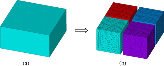
FETI-DP 구현의 경우 원래 계산 영역 Ω이 먼저 겹치지 않는 일련의 하위 영역 Ωi으로 분할됩니다.
(나 =1, 2, 3⋯, Ns ), 그림 1과 같이 각 하위 도메인에서 Ωi
, 하위 도메인 유한 요소 시스템은 벡터 파동 방정식에서 다음과 같이 유도될 수 있습니다.
FETI-DP 방식에서 겹치지 않는 하위 도메인이 있는 도메인 분할 방식. 아 원래 도메인. ㄴ 분할된 하위 도메인 및 이산화된 메시
여기서 E나
\( {\Omega}^i \), k로 풀어야 할 미지의 전기장을 나타냅니다. 0 그리고 η0 는 각각 자유 공간 파수와 고유 임피던스이고 \( {\mathbf{J}}_i^{\mathrm{imp}} \) 는 가해진 전류입니다. \( {\Gamma}_{\mathrm{ABC}}^i \)는 무한 개방 영역을 자르기 위한 흡수 경계 조건(ABC)을 의미합니다. k0 주변 매체가 광학 트래핑에 일반적인 자유 공간이 아닌 경우 매체의 파동 임피던스로 대체되어야 합니다. 하위 도메인 인터페이스 Γi에서
, 가정된 경계 조건은 Ωi에서 완전한 경계 값 문제를 생성하는 데 필요합니다.
. 여기서, 알 수 없는 보조 변수 Λ를 갖는 로빈형 전송 조건 나 다음과 같이 부과됩니다.
여기서 \( {\hat{n}}^i \)는 하위 도메인 인터페이스 Γi에서 단위 법선 바깥쪽 벡터를 나타냅니다.
, 및 α나
종종 jk로 선택할 수 있는 복잡한 매개변수입니다. 0 . 모든 하위 도메인은 사면체 요소에 의해 이산화됩니다. 각 요소에서 E를 확장합니다. 벡터 기본 함수 N 사용 및 미지의 전기장 계수 E 로
여기서 아래 첨자 표기법 c 그리고 r 모서리 자유도(DOF)와 나머지 DOF를 구별하여 모서리 DOF를 원시 변수로 추출하여 이중 원시(DP) 체계를 구성합니다. 자, 케이 FEM 시스템 행렬 및 f 여기 벡터입니다. 나 하위 도메인의 인터페이스 DOF를 추출하는 부울 행렬입니다. λ 확장 Λ에서 생성된 이중 변수입니다. 나 , 라그랑주 승수라고도 합니다.
그런 다음 경계면에서 접선 전기장 및 자기장 연속성을 적용하여 인접한 하위 도메인을 상호 연결할 수 있습니다. 우리는 모든 하위 도메인 인터페이스를 어셈블하고 모든 하위 도메인 내부 미지수 E를 제거합니다. 나
. 이중 변수 λ에 대한 축소된 전역 인터페이스 방정식 다음과 같이 얻을 수 있습니다.
식 (6)은 GMRES(Generalized Minimum Residual) 방법과 같은 반복적인 방법으로 풀 수 있습니다. \( {\tilde{\mathbf{K}}}_{cc} \) 는 원시 공간에서 반복 수렴을 가속화할 수 있는 전역 모서리 시스템입니다. 근사 역 및 불완전 LU 분해와 같은 반복 수렴 속도를 개선하기 위해 적절한 선조건자를 사용할 수 있습니다. 일단 이중 변수 λ 가 해결되면 각 하위 영역 내부의 전기장은 (5)에 의해 독립적으로 평가될 수 있습니다. 전역 행렬 \( {\tilde{\mathbf{K}}}_{rr} \)의 구성을 위해 하위 도메인 수치 Green의 함수 \( {\mathbf{Z}}_{rr}^ 나는 \)
형식으로 $$ {\mathbf{Z}}_{rr}^i={\mathbf{B}}_r^i{\left({\mathbf{K}}_{rr}^i\right)}^{- 1}{{\mathbf{B}}_r^i}^T $$ (7)
여기서 하위 도메인 FEM 행렬 \( {\left({\mathbf{K}}_{rr}^i\right)}^{-1} \)의 역행렬이 포함됩니다. 게다가 행렬 \( {\tilde{\mathbf{K}}}_{rc} \), \( {\tilde{\mathbf{K}}}_{cr} \) 및 \( {\tilde {\mathbf{K}}}_{cc} \) 및 벡터 \( {\tilde{f}}_r \) 및 \( {\tilde{f}}_c \), \( {\left({ \mathbf{K}}_{rr}^i\right)}^{-1} \)를 계산해야 합니다. 전처리 단계에서 \( {\left({\mathbf{K}}_{rr}^i\right)}^{-1} \) 의 구성과 다음에서 행렬-벡터 곱(MVP) 반복 솔루션 단계는 계산 비용이 많이 듭니다. \( {\mathbf{K}}_{rr}^i \) 는 희소하지만 \( {\left({\mathbf{K}}_{rr}^i\right)}^{-1} \ ) 밀도가 높기 때문에 계산 비용이 많이 듭니다. 다음으로 \( {\left({\mathbf{K}}_{rr}^i\right)}^{-1} \)의 계산을 가속화하기 위해 낮은 순위의 희소화 방법이 도입되었습니다. 전역 인터페이스 시스템의 일부 부분행렬은 하위 행렬 형태로 표현될 수 있으므로 하위 행렬의 계산은 FETI-DP의 성능을 향상시키는 하위 알고리즘으로 수행될 수 있습니다. FETI-DP는 독립적인 하위 영역 작업을 제공하므로 병렬 계산을 활용하여 효율성을 높일 수 있음을 알 수 있습니다. 효율적인 병렬 방식을 위해 도메인 분할의 원칙은 각 하위 도메인의 DOF 수를 최대한 균형 있게 만드는 것입니다. 따라서 하위 도메인의 크기는 메쉬 이산화 밀도와 관련되어야 합니다. 일반적으로 작은 하위 도메인은 미세한 메쉬 영역에 채택되고 큰 하위 도메인은 조잡한 메쉬 영역에 채택됩니다.
낮은 순위 희소화
FETI-DP 효율성을 개선하기 위해 데이터 희소 방법을 제공하기 위해 낮은 순위 성소 접근 방식이 제안됩니다. 여기, 데이터가 희박한 이는 이러한 행렬이 실제로 희소하지 않다는 것을 의미하지만 그 행렬의 특정 하위 블록이 다음과 같이 낮은 순위의 분해 행렬 형식으로 표현될 수 있다는 점에서 희소합니다.
여기서 X 및 Y 전체 행렬 형식이고 순위 km보다 훨씬 작습니다. 그리고 n . 행렬 \( {\left({\mathbf{K}}_{rr}^i\right)}^{-1} \)는 적분의 행렬 속성을 가지므로 데이터 희소 행렬 형식으로 나타낼 수 있습니다. 운영자. 따라서 \( {\left({\mathbf{K}}_{rr}^i\right)}^{-1} \) 주어진 하위 도메인에서 낮은 순위 속성을 가지고 있으면 효율적으로 계산되고 저장될 수 있습니다. 반복적인 솔루션에서 MVP를 가속화하는 낮은 순위의 희소화 접근 방식을 사용하는 데이터 희소 형식.
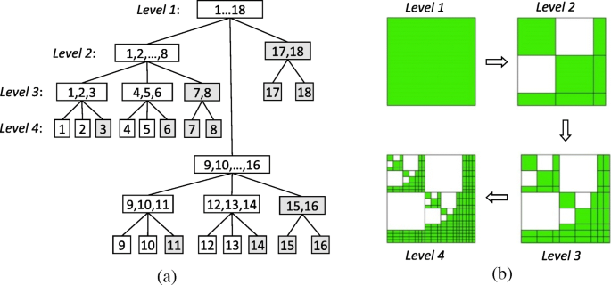
낮은 순위의 희소화 접근법의 과정은 다음과 같은 단계로 나눌 수 있다:(1) 각 서브도메인에 설정된 기저 함수를 세분화하여 클러스터 트리를 구성하고, (2) 두 클러스터 트리의 상호 작용을 통해 블록 클러스터 트리를 구성한다. 3) 허용 조건에 의해 데이터 희소 형식 \( {\mathbf{K}}_{rr}^i \) 생성, (4) 낮은 순위 형식의 알고리즘을 수행하여 \( {\left({\mathbf{K}}_{rr}^i\right)}_{\mathrm{DS}}^{-1} \), (5) 다음과 같이 FETI-DP 시스템의 해를 입력합니다. 데이터 희소 알고리즘. 솔루션의 속도를 높이기 위해 적절한 사전 조절기를 사용할 수 있습니다. 데이터 희소 LU 분해 \( {\left({\mathbf{K}}_{rr}^i\right)}_{\mathrm{DS}}={\left({\mathbf {L}}_{rr}^i\right)}_{\mathrm{DS}}{\left({\mathbf{U}}_{rr}^i\right)}_{\mathrm{DS} } \)는 행렬 반전 \( {\left({\mathbf{K}}_{rr}^i\right)}_{\mathrm{DS}}^{-1} \)을 대체하기 위해 채택되었습니다. 로우 랭크 스파스화의 효율성을 더욱 향상시키기 위해 중첩 해부 기술이 사용됩니다. 중첩된 해부는 구분자를 사용하여 큰 비대각선 0 하위 블록을 생성합니다. 이 하위 블록은 LU 분해 중에 0을 유지하므로 필인을 크게 줄일 수 있습니다.
\( {\left({\mathbf{K}}_{rr}^i\right)}_{\mathrm{DS}} \)를 생성하려면 먼저 클러스터 트리 T를 구성합니다. 나 하위 도메인 에지 기반 기본 함수 집합 I의 재귀적 세분화에 의해 ={1,2,…N } 경계 상자를 사용합니다. 중첩된 해부로 클러스터 t 해당 경계 상자 내에서 세 개의 후속 항목 {s으로 나뉩니다. 1 , s9월 , s2 }, 여기서 s1 그리고 s2 두 개의 연결이 끊긴 경계 상자와 s의 인덱스 집합입니다. 9월 구분 기호의 인덱스 집합입니다. 그림 2a는 이 프로세스의 간단한 예를 보여줍니다. 그런 다음 블록 클러스터 트리 T나 × 나 두 개의 클러스터 트리 T를 상호 작용하여 구성할 수 있습니다. 나 , 그림 2b와 같이 원래 edge-based 기저 함수 집합의 클러스터 트리와 Galerkin의 방법에서 설정한 테스트 기저 함수 집합의 클러스터 트리로 선택할 수 있습니다. 다음으로, T에서 전체 블록, 하위 분해 블록 및 비대각 제로 블록을 구별하기 위해 중첩 해부에 기반한 허용 조건을 도입해야 합니다. 나 × 나 [23]. 따라서 \( {\left({\mathbf{K}}_{rr}^i\right)}_{\mathrm{DS}} \) 는 해당 블록을 0이 아닌 항목으로 채워서 생성할 수 있습니다. \( {\mathbf{K}}_{rr}^i \). 마지막으로, \( {\left({\mathbf{K}}_{rr}^i\right)}_{\mathrm{DS}}={\left({\mathbf{L }}_{rr}^i\right)}_{\mathrm{DS}}{\left({\mathbf{U}}_{rr}^i\right)}_{\mathrm{DS}} \ )는
에서 재귀적으로 계산할 수 있습니다. $$ {\mathbf{K}}_{rr}^i=\left[\begin{array}{ccc}{\mathbf{K}}_{11}&&{\mathbf{K}}_{13 }\\ {}&{\mathbf{K}}_{22}&{\mathbf{K}}_{23}\\ {}{\mathbf{K}}_{31}&{\mathbf{K }}_{32}&{\mathbf{K}}_{33}\end{array}\right]=\left[\begin{array}{ccc}{\mathbf{L}}_{11}&&\\ {}&{\mathbf{L}}_{22}&\\ {}{\mathbf{L}}_{31}&{\mathbf{L}}_{32}&{\mathbf{ L}}_{33}\end{array}\right]\left[\begin{array}{ccc}{\mathbf{U}}_{11}&&{\mathbf{U}}_{13} \\ {}&{\mathbf{U}}_{22}&{\mathbf{U}}_{23}\\ {}&&{\mathbf{U}}_{33}\end{배열} \right] $$ (9) <그림>
내포해부 기반의 4단계 클러스터 트리 및 블록 클러스터 트리 구성. 아 에지 기반 기본 함수 집합 I의 재귀 세분화에 의한 클러스터 트리 구성 ={1,2,…18}. ㄴ흰색 블록 클러스터 트리 구성 블록은 0행렬이고 녹색입니다. 블록은 전체 행렬 또는 하위 분해 행렬일 수 있습니다.
여기서 기존의 전체 행렬 산술은 데이터 희소 대응으로 대체됩니다[28]. 적응 잘림 오류 ε그 낮은 순위 근사의 정확도를 제어하는 데 사용됩니다. 구한 LU 인수 \( {\left({\mathbf{L}}_{rr}^i\right)}_{\mathrm{DS}} \) 및 \( {\left({\mathbf{U} }_{rr}^i\right)}_{\mathrm{DS}} \) 는 저장되고
에 의해 \( {\mathbf{Z}}_{rr}^i \)를 구성하는 데 사용됩니다. $$ {\mathbf{Z}}_{rr}^i={\mathbf{B}}_r^i{\left({\mathbf{U}}_{rr}^i\right)}_{\ mathrm{DS}}^{-1}{\left({\mathbf{L}}_{rr}^i\right)}_{\mathrm{DS}}^{-1}{\mathbf{B} }_r^i $$ (10)
여기서 \( {\mathbf{B}}_r^i{\left({\mathbf{U}}_{rr}^i\right)}_{\mathrm{DS}}^{-1} \) 및 \( {\left({\mathbf{L}}_{rr}^i\right)}_{\mathrm{DS}}^{-1}{\mathbf{B}}_r^i \) 데이터 희소 상부 및 하부 삼각 솔버에 의해 계산됩니다. \( {\left({\mathbf{L}}_{rr}^i\right)}_{\mathrm{DS}} \), \( {\left({\mathbf{U}}_{ rr}^i\right)}_{\mathrm{DS}} \) 및 \( {\mathbf{Z}}_{rr}^i \) 앞뒤로 데이터가 희박한 FETI-DP 계산을 입력합니다. 대체(FBS) 및 데이터 희소 MVP.
광학력 및 잠재력
전기역학 이론에 따르면 광학적 힘은 전자기장과 기계적 운동량 사이의 관계를 나타내는 Maxwell 응력 텐서(MST)에 의해 평가될 수 있습니다[29]. 물체 주변의 전자기장 분포가 얻어지면 물체를 둘러싼 닫힌 표면에 대해 MST를 적분하여 광학력을 계산할 수 있습니다. 얻은 전기장 분포를 기반으로 모든 좌표에서 MST는 다음과 같이 구성할 수 있습니다.
여기서 위 첨자 별표는 전기장 또는 자기장의 켤레를 나타냅니다. εμ입니다 는 유전율과 투자율이며 \( \overleftrightarrow{\mathbf{I}} \) 는 3 × 3 단위 행렬입니다. 벡터의 외적에 의해 \( \overleftrightarrow{\mathbf{T}} \) 의 텐서 형식은 다음과 같이 쓸 수 있습니다.
마지막으로 물체에 가해지는 광학적 힘은 물체를 둘러싸고 있는 닫힌 표면에 대해 MST를 적분하여 계산할 수 있습니다.
$$ \mathbf{F}={\oint}_S\left(\overleftrightarrow{\mathbf{T}}\cdot \hat{n}\right)\ dS. $$ (15)
MST의 적분은 해당 하위 도메인에 할당되기 때문에 광학력의 계산은 병렬로 구현될 수도 있습니다. 안정적인 광학 트래핑을 위해 주요 조건 중 하나는 기울기 힘이 산란력보다 커야 한다는 것입니다. 즉, 전체 힘의 방향은 항상 전기장의 세기가 가장 강한 위치를 가리키는 기울기 힘의 방향과 같아야 합니다.
광 포텐셜은 광 트래핑의 안정성을 나타내는 또 다른 매력적인 매개변수입니다. 얻어진 광학력을 기반으로, 광학 전위 깊이 U 위치 r에서 0
로 계산할 수 있습니다. $$ \mathbf{U}\left({r}_0\right)=-{\int}_{\infty}^{r_0}\mathbf{F}\left(\mathbf{r}\right)\cdot \mathbf{r}, $$ (16)
여기서 첨자 ∞는 전위가 0인 기준점으로 정의된 무한대를 나타냅니다. U 값 k로 나타낼 수 있습니다. 나 T, 여기서 k나 1.3806488 × 10
−23
의 볼츠만 상수를 나타냅니다. J/K 및 T는 주변 온도입니다. 일반적으로 입자는 용액에서 브라운 운동을 극복하고 U일 때 안정적으로 갇힐 수 있습니다.> 1 k나 T 만족합니다. 그렇지 않으면 입자를 안정적으로 가둘 수 없습니다. 총 광학력은 보존적 경사력 성분과 비보존적 산란력 성분을 포함하므로 총 광학력 F (15)에서 나온 것은 보수적이지 않다[30, 31]. 그러나 나노입자의 움직임이 한 차원으로 제한된다면 전체 광학력이 비보존적임에도 불구하고 이것은 (16)에서 광학 전위의 명확한 정의를 산출합니다.
결과 및 토론
제안된 방법의 효과를 입증하기 위해 세 가지 예가 제시됩니다. 귀금속은 일반적으로 표면 플라즈몬을 여기시키는 데 사용되기 때문에 분석을 위해 대표적인 금과 은 재료를 선택합니다. 첫 번째 예는 제안된 방법의 정확성을 검증하기 위해 은 나노입자의 광학적 힘을 계산한다. 두 번째 및 세 번째 예는 금 나노 입자의 광학 트래핑을 시뮬레이션하고 논의합니다. 모든 예에서 무한 영역은 ABC로 잘리고 ABC와 물체 사이의 거리는 허용 가능한 정확도를 달성하기에 충분한 하나의 파장으로 설정됩니다. 모든 계산은 3.6 GHz Intel Xeon 프로세서가 장착된 Dell 워크스테이션에서 수행됩니다.
실버 나노캡슐
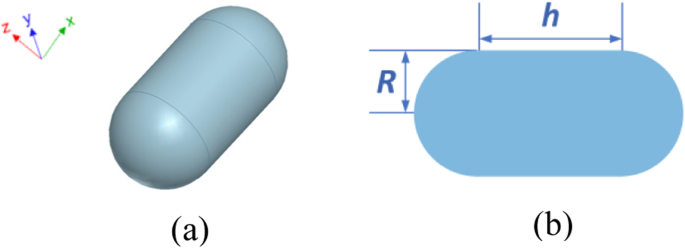
은 나노캡슐 물체는 광학력 예측에서 제안된 FETI-DP 방법의 정확도와 효율성을 테스트하기 위해 먼저 고려됩니다. 그림 3a 및 b는 구성 및 치수를 나타냅니다. 은의 구성 매개변수는 모두 [32]에서 가져온 측정값입니다. FETI-DP 방식을 구현하기 위해 먼저 전체 분석 영역을 24개의 하위 영역으로 나눕니다. 플라즈몬 로컬 필드 향상 효과를 모델링하려면 금속 표면 근처에서 더 조밀한 메쉬가 필요합니다. 이산화를 위해 사면체 요소가 채택되어 총 6.9 × 10
5
이 됩니다. 미지수(4.1 × 10
4
포함) 이중 미지수 및 313 코너 미지수. 입사광은 +z 방향을 따라 조명됩니다. , 전기장의 분극 방향은 -x .
<그림>
은 나노캡슐 구조의 구성. 아 3D보기. ㄴ 정면도 및 치수, 여기서 R =30 nm 및 h =60 nm
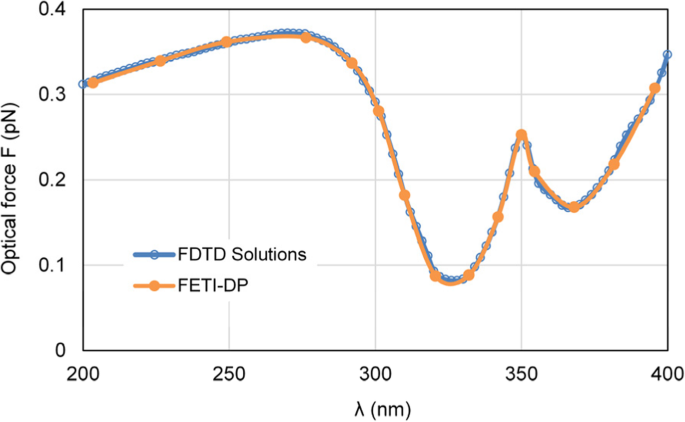
먼저 입사광 λ의 파장을 변경합니다. 나노캡슐에 가해지는 광학적 힘을 시뮬레이션하기 위해 200 nm에서 400 nm까지. FETI-DP는 주파수 영역에서 작동하므로 광학력은 15개의 샘플링 주파수 지점에서 계산됩니다. 그림 4는 은 나노캡슐에 가해진 광학력의 계산된 곡선을 보여줍니다. FETI-DP의 정확도를 나타내기 위해 FETI-DP의 광학력 결과를 상용 소프트웨어 Lumerical FDTD Solutions[33]의 결과와 비교하고 좋은 일치를 관찰할 수 있습니다.
<사진>
파장 λ에 따라 달라지는 은 나노캡슐에 가해진 광학적 힘의 결과 FETI-DP 및 상용 소프트웨어 FDTD 솔루션의 결과를 포함한 입사광
Then, the performance of FETI-DP is tested for different numbers of subdomains. We increase the number of subdomains from 4 to 24 by keeping the discretization density. We assign each processor to deal with one subdomain. Table 1 reports the time used for the construction of global interface Eq. (6) and the total solution time. It can be seen that the FETI-DP can fully exploit parallel computing resources and significantly improve the solution efficiency. Besides, the accuracy of the FETI-DP with the number of subdomains increasing is also examined and reported in Table 1. Here, the accuracy is defined by the 2-norm relative error of the optical force as δOF = ‖OF나 − OFref ‖/‖OFref ‖, where OF나 is the optical force using i subdomains and OFref denotes the reference optical force using two subdomains. It can be seen that the accuracy keeps almost constant with the number of subdomains increasing.
Gold Nanosphere Dimer
The second example analyzes the optical trapping of a gold nanosphere by using a gold nanosphere dimer. The plasmonic effects at the dimer gap can effectively enhance the optical force for trapping nanoparticle. Figure 5 a and b gives the configuration and dimensions of this system. The constitutive parameters of gold are all measured values taken from [32]. The surrounding medium is water with a relative refractive index of n = 1.33. The incident light is a plane wave with the power of 10 mW/μm
2
, the electric field polarization direction is +x , and the incident direction is −z . The optical force exerted on the object nanosphere is calculated by the FETI-DP method. For the FETI-DP implementation, the whole computational domain is divided into 32 subdomains and discretized by tetrahedral meshes, which results in 3.5 × 10
6
unknowns, including 1.6 × 10
5
dual unknowns and 1738 corner unknowns.
Configuration of an optical trapping system of a gold nansphere dimer in water. 아 3D view. ㄴ Front view and dimensions, where R = 25 nm, r = 5 nm, and g = 2 nm
First, we test the parallel performance of the proposed FETI-DP by using various numbers of processors. Table 2 reports the solution time for Eq. (6) as well as the total solution time. Besides, the speedups for the parallel computation are also provided in Table 2. Here, the speedup is defined by
where \( {T}_{N_p} \) denotes the total wall-clock time using Np processors. It can be seen that the FETI-DP significantly improves the solution efficiency and exhibits good parallel speedup. For this large number of unknowns, the total memory usage of all the processors is only 57.2 GB.
Then, the effectiveness of the low-rank sparsification approach is examined. With the low-rank sparsification, the subdomain matrix can be factorized by data-sparse algorithm and stored as data-sparse matrices. The construction time and memory usage are only 18 s and 0.5 GB, while they are 67 s and 1.7 GB by conventional matrix algorithm. It can be seen that we get 72% time saving and 70% memory compression. Related to the memory usage, the subsequent MVPs can also get 70% time-saving.
Next, the FETI-DP is tested for the optical force calculation with the wavelength λ varying from 277 nm to 818 nm. In practice, the analyses of optical force under incident light of different wavelengths are often necessary for searching the plasmonic resonance wavelength, where drastic field enhancement occurs and the strongest optical force can be obtained. Two cases are considered with the nanosphere located at (0, 0, 20 nm) and (0, 0, − 20 nm). Figure 6 a and b plots the calculated optical forces exerted on the nanosphere for different λ . It can be seen that the maximum optical force occurs at λ = 472 nm, which is the plasmonic resonance wavelength. The optical force at this resonance wavelength enhanced by nearly 40 times as against that at non-resonance wavelength. Moreover, the optical force always points to the dimer gap, as shown in Fig. 6, where the electric field intensity is strongest. It is also the direction of gradient force to trap the object. Figure 7 a and b shows the calculated electric field enhancement distributions at the non-resonance wavelength of λ = 300 nm and the resonance wavelength of λ = 472 nm, respectively. It can be seen that the electric field intensity has been increased by almost 250 times due to the plasmonic resonance effect.
Calculated results of optical forces exerted on the nanosphere in the system of gold nanosphere dimer, varying with the wavelength λ of incident light. 아 The object nanosphere is located at (0, 0, 20 nm). ㄴ The object nanosphere is located at (0, 0, − 20 nm)
The electric field enhancement distributions on the xoz plane for the system of gold nanosphere dimer. 아λ = 300 nm (non-resonance wavelength). ㄴλ = 472 nm (resonance wavelength)
Besides, the optical force and optical potential are calculated with the nanosphere moving from (0, 0, − 30 nm) to (0, 0, − 17 nm) along the z -중심선. Since the most typical and interesting behavior of trapping forces and potentials are those acting along z -direction, we here consider the axial trapping potential by integration along the z -중심선. Because the motion of the nanoparticle is restricted to one dimension, the definition of an optical potential is unambiguous from (16), even though the total optical force from (15) is non-conservative. As shown in Fig. 8 a, b, with the nanosphere moving to the dimer gap, the optical force and optical potential depth obviously increase. At the position of (0, 0, − 17 nm), an optical potential depth of 4.6 k나 T is produced, which is sufficient to overcome the Brownian motion in water to achieve stable optical trapping.
The optical forces and optical potentials exerted on the nanosphere in the system of gold nanosphere dimer, when the nanosphere moves from (0, 0, − 30 nm) to (0, 0, − 17 nm). 아 The optical forces. ㄴ The optical potentials
Finally, we test the effects of the dielectric substrate for this example. The optical forces are calculated with and without a substrate, respectively. For both two cases, the nanosphere is located at (0, 0, − 20 nm) and the incident wavelength is chosen as the resonance wavelength. For the case without substrate, the calculated result of the optical force is |F0 | = 0.769 pN. For the case with a substrate, the gold nanosphere dimer is put on a dielectric substrate with a thickness of 60 nm and a relative permittivity of εr = 2.25. The calculated result of the optical force is |F1 | = 0.761 pN. The relative error between these two results of optical forces is about 1.0 × 10
−2
, which is defined as |F1 − F0 |/|F0 |.
Gold Truncated Cone Dimer
The third example deals with the optical trapping of a gold nanosphere by using a gold truncated cone dimer. Figure 9 gives the configuration and dimensions of this system. The constitutive parameters of gold are taken from [32]. The dielectric substrate has a relative permittivity of εr = 2.25. The surrounding medium is water with a relative refractive index of n = 1.33. The incident light is plane wave with the power of 10 mW/μm
2
, the electric field polarization direction is +x , and the incident direction is −z . The whole computational domain is divided into 32 subdomains and discretized by tetrahedral meshes, which leads to 3.1 × 10
6
unknowns, including 1.3 × 10
5
dual unknowns and 1227 corner unknowns.
Configuration of an optical trapping system of a gold truncated cone dimer based on a dielectric substrate in water. 아 3D view. ㄴ Front view and dimensions, where UR = 20 nm, LR = 30 nm, h = 35 nm, and g = 2 nm
First, we analyze the optical forces by changing λ from 277 nm to 818 nm. Figure 10 plots the calculated optical forces exerted on the nanosphere for different λ . The nanosphere is located at (0, 0, 35 nm). It can be seen that the maximum optical force occurs at λ = 464 nm, which is the plasmonic resonance wavelength, and the optical force here is enhanced by nearly 30 times at non-resonance wavelength. Moreover, the total optical force always points to −z , as shown in Fig. 10, which is the direction of the gradient force. This confirms that the gradient force is greater than the scattering force, which is one of the conditions that the nanosphere can be stably trapped. Figure 11 a and b presents the calculated electric field distributions at the non-resonance wavelength of λ =300 nm and the resonance wavelength of λ = 464 nm, respectively. It can be seen that electric field intensity has been increased by almost 500 times due to the localized surface plasmon resonance.
Calculated results of optical forces exerted on the nanosphere in the system of gold truncated cone dimer, varying with λ . The nanosphere is located at (0, 0, 35 nm)
The electric field enhancement distributions on the xoz plane for the system of gold truncated cone dimer. 아λ =300 nm (non-resonance wavelength). ㄴλ =464 nm (resonance wavelength)
Then, the location of the nanosphere is changed to 0, 5, and 35 nm to observe the optical force. Figure 12 gives the calculated optical forces exerted on the nanosphere, where obvious y -component of optical force can be observed, while greater z -component of optical force exists. The total optical force still points to the position with the strongest electric field to trap the nanosphere.
Calculated results of optical forces exerted on the nanosphere in the system of gold truncated cone dimer varying λ . The nanosphere is located at (0, 5 nm, 35 nm)
Furthermore, we analyze the optical potential with the nanosphere moving from (0, 0, 50 nm) to (0, 0, 20 nm) along the z -중심선. Here, we consider the axial trapping potential along z -direction, which restricts the motion of the nanoparticle to one dimension and leads to an unambiguous definition of optical potential. Both the optical force and potential are calculated. As can be observed from Fig. 13 a, b, with the nanosphere moving to the dimer gap, the optical force and the optical potential depth obviously increase. At (0, 0, 20 nm), an optical potential depth of 3.8 k나 T is obtained, which is sufficient to overcome the Brownian motion in water to achieve stable optical trapping.
The optical forces and optical potentials exerted on the nanosphere in the system of gold truncated cone dimer, when the nanosphere moves from (0, 0, 50 nm) to (0, 0, 20 nm). 아 The optical forces. ㄴ The optical potentials
Finally, we test the computational costs of the FETI-DP by changing the number of unknowns from 1.0 million to 3.2 million based on different mesh size. In practice, the tests under different mesh density are usually necessary to meet different accuracy requirements. Such a large-scale complex problem brings great challenges to conventional numerical methods. However, the FETI-DP can easily handle this problem. Thirty-two processors are employed for the FETI-DP simulation, while each processor deals with a subdomain. Table 3 reports the computational costs of the FETI-DP. It can be seen that the FETI-DP exhibits high simulation efficiency and low memory requirement.
결론
An FETI-DP method combined with low-rank sparsification is proposed for the prediction and analysis of optical trapping of metal nanoparticles. The proposed method provides fully decoupled subdomain problems, which converts a large-scale complex problem into a series of small-scale simple problems. It is well-suited for parallel computation and can significantly improve the efficiency of numerical simulation. Examples demonstrate that the proposed method exhibits excellent performance of large-scale computation and is well-suited for the fast and accurate simulation of optical trapping at nanoscale.
데이터 및 자료의 가용성
All data generated or analyzed during this study are included in this article.
약어
ABC:
Absorbing boundary condition
DOF:
Degrees of freedom
FDTD:
유한 차분 시간 영역
FEM:
Finite element method
FETI-DP:
Dual-primal finite element tearing and interconnecting