Owing to their small physical size and low power consumption, RRAM devices are potential for future memory and logic applications. Increased storage density is among the most critical aspects of memory technology to enable the design of multibit capacity [89] memory cells. The multiple resistive states can be achieved in RRAM cells which provide benefits of low-cost and high-density non-volatile data storage solutions. Currently, a lot of research is being conducted in the area of RRAM to scale down the dimensions and increase the structural density of memory arrays. Previously, the storage density of RRAM has been increased by the reduction of device size; however, the complexity involved in the experimental procedures limits its successful implementation. Another suggested method is employing three-dimensional (3D) crossbar architectures. Two types of architectures of ‘vertical’ and ‘crossbar RRAM’ have been proposed [116, 117]; however, both these architecture types require advanced fabrication procedures which is not desirable. A much simpler alternative to increase storage density in RRAM devices is by making use of multilevel cell (MLC) storage technology which enables storing more than one bit per cell without reducing the physical device dimensions. This MLC is one of the most promising properties of RRAM which can significantly increase the memory storage density [83, 118–125]. Thus, instead of a single high and low resistance state (HRS and LRS), we can achieve multiple HRS and LRS, without changing the device dimensions. However, to achieve reliable MLC operation, the precise control over the resistance of the different resistance levels of RRAM should be ensured; otherwise, the device will suffer from resistance variability and reliability issues mainly due to the random nature of the conductive filament formation during the switching process [126].
The MLC behavior in RRAM makes it very useful for high-density applications. To obtain MLC behavior in RRAM, the following three methods are employed:(i) changing compliance current, (ii) controlling reset voltage and (iii) varying pulse width of program/erase operation.
The RRAM device is usually operated with 1-RRAM (1R) cell configuration [41] or in 1-Transistor 1-RRAM (1T-1R) cell configuration [18]. The MLC characteristics in 1R configuration can be obtained by changing the current compliance (I cc ) during ‘set’ operation whereas the MLC characteristics in 1-Transistor 1-RRAM (1T-1R) cell structure are controlled by varying the voltage at the gate of the transistor, which enables the control of compliance current (I cc ) during the set operation of a RRAM cell. The typical MLC I-V curves of Ti/Ta2 O5 /Pt [127] based RRAM cell are shown in Fig. 11. As the compliance current (I cc ) is increased from 150 μ A to 1 mA, six different LRS are obtained at I cc =150 μ A, I cc =200 μ A, I cc =300 μ A, I cc =500 μ A and I cc =700 μ A, I cc =1 mA due to the increase in the respective current of LRS (I LRS ) while the HRS is maintained constant and the HRS current (I HRS ) remains same for all the LRS levels. For Ti/Ta2 O5 /Pt RRAM, with the increase in I cc , the maximum reset current (I reset ) also increases while the set voltage is almost maintained constant. Also, it was observed that the resistance of the LRS (R LRS ) decreases while the (I reset ) increases owing to the stronger filament formation with the increase in I cc .
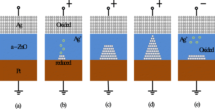
Schematic illustration of multiple resistance states in RRAM cell obtained by varying compliance current ‘I cc ’ [98]
The MLC characteristics in a RRAM cell can also be obtained by controlling the reset voltage (V reset ) while (I cc ) is maintained constant. In this case, the typical MLC I-V curves of TiN/HfO x /AlO x /Pt-based RRAM cell [128] by applying different (V reset ) of − 2.1 V, − 2.7 V and − 3.3 V are shown in Fig. 13.
Schematic illustration of multiple resistance states in RRAM cell obtained by varying reset voltage ‘V reset ’ [98]
MLC characteristics can also be obtained by varying the program/erase pulse width while the amplitude of the pulse is maintained constant [23]. In HfO x -based RRAM [128], three HRS levels were demonstrated by varying the width of the reset pulse from 50 ns to 5 μ 에스. This method of obtaining MLC characteristics in RRAM is relatively easier; however, this scheme is energy inefficient. This drawback limits the application of this method to obtain reliable characteristics in the RRAM cell. The higher energy consumption of the RRAM device was confirmed on the comparison of the transient responses between the reset pulse amplitude and pulse width control. This is particularly due to the higher unwanted energy dissipation as the thermal energy in the resistive switching material.
A summary of RRAM devices exhibiting multiple resistance states is shown in Table 4. As is evident from the table, various RRAM devices with multiple resistance states have been reported. Till date, however, only 8 resistance states have been demonstrated in a single RRAM cell either by varying I cc or V reset . Therefore, there is a huge scope for increasing the number of resistance states in the RRAM cell, thus enhancing its storage density.
Modeling of RRAM Devices
Modeling plays a very critical role in development of devices utilizing semiconductor technologies. To fully understand device operation and to optimize the performance, an accurate model is of great importance. A number of RRAM models with varying features and accuracy have been proposed [129]. This section discusses the characteristics and attributes of the various commonly used RRAM models popular.
Stanford/ASU Model
One of the most popular physics-based RRAM models is the Stanford/ASU RRAM model [130–132], proposed by Guan et al. and Chen et al. This model was applied to validate the I-V switching characteristics of HfO2 RRAM [128] and includes the effect of Joule heating and temperature change on the switching of RRAM devices.
This model is dependent on the CF growth inside a dielectric switching layer. The filament gap, i.e. the gap between the tip of the CF and top electrode, is the internal state variable for this model. The growth of CF inside a dielectric is attributed to the oxygen ion movement and regeneration and recombination of oxygen vacancies [133]. Thus, the rate of change of filament gap (g) is given as [130]:
$$ {\frac{dg}{dt}} =V_{\tiny{0}}.\exp\bigg({{\frac{-E_{a},m}{k_{b}.T}} }\bigg). {\text{Sinh}} \bigg({\frac{qa_{h}\gamma V}{L.k_{b}.T}}\bigg) $$ (1)
여기서 E a is the activation energy, V is the magnitude of the voltage applied across the device, L is the switching material thickness, a h is the hopping distance, γ is the local field enhancement factor, V 0 is the velocity containing attempt to escape frequency, K b is the Boltzmann constant, q is the elementary unit charge and T is the temperature of the conductive filament.
The spatial variation in the gap size is accounted for in this model, in addition to the variations which arise due to the stochastic property of the ion process. A noise signal is added to the gap distance to account for these variations as [130]:
$$ g_{|t+\Delta t} =F \Big[ g_{|t}, {\frac{dg}{dt}} \Big] + \delta_{g}\times\tilde{X}(n)\Delta t, n ={\frac{t}{T_{GN}}} $$ (2)
여기서 Δ t is the simulation time step, the function F represents time evolution of gap size fromt to Δ 티. \(\tilde {X}\)(n) is a zero mean Gaussian noise sequence. 티 GN is the time interval after which \(\tilde {X}\)(n ) changes to next random value.
The variation in the gap size δ g depends on kinetic energy of ions and filament temperature as [130]:
$$ \delta_{g} (T) ={\frac{\delta^{\tiny{0}}_{g}}{\bigg\{ 1+\exp \Big({\frac{T_{\text{crit}}- T}{T_{\text{smith}}}} \Big) \bigg\}}} $$ (3)
where \(\delta ^{0}_{g}\) and T smith are fitting coefficients to match the resistance distribution curves to experiments and T crit is a threshold temperature above which the gap size changes significantly.
This model shows strong dependence on temperature; thus, there is a need to account for the change of ‘T’ . With change in cell characteristics, the dynamic inner domain temperature T changes significantly, while the outer domain assumed to be at uniform and stable temperature (T bath ), is related as [130]:
$$ c_{p} {\frac{dT}{dt}} =V(t).I(t) - k(T-T_{\text{bath}}) $$ (4)
where C p is the effective heat capacitance of inner domain, V (t) I (t) represents the Joule heating and k is the effective thermal conductivity.
Using a generalized conduction mechanism, the current conduction is defined as [130]:
$$ I(g,v) =I_{\tiny{0}}.\exp\bigg({{\frac{-g}{g_{\tiny{0}}}} }\bigg){\text{Sinh}} \bigg({\frac{V}{V_{\tiny{0}}}}\bigg) $$ (5)
나 0 , g 0 및 V 0 are the fitting parameters to match experimental results.
One of the significant features of this model is its implementation in neuromorphic applications and RRAM synaptic device design [134], giving the model a great degree of flexibility and further scope for implementation in various neuromorphic systems.
Physical Electro-thermal Model
Physical electro-thermal model was developed by Kim et al. [135] and implemented with tantalum pentoxide (Ta2 O5 ) -based bilayer RRAM [136–138]. This physical model solves the differential equations based on finite element solving method. This model also makes use of electrothermal physics phenomenon approach for modeling [139], thus giving it advantage in terms of flexibility to incorporate finite element method (FEM) solver to simulate the system very accurately. However, the drawback of this approach is its difficulty in implementation for SPICE and Verilog circuit solvers.
This model describes CF as a doped region having oxygen vacancies as dopants with CF extending from the top to the bottom electrode of the device. To describe the drift-diffusion of vacancy migration, this model assumes the same equation can be used to describe both the processes of oxygen ions and vacancies. The ion model by Mott and Gurney [140] is employed here to describe the process given as [135]:
$$ {\frac{dn_{D}}{dt}} =\Delta \times \bigg(D_{s}.\Delta_{n\tiny{D}}- \mu v n_{D} \bigg) + G $$ (6)
where D s describes the diffusion process, v gives the drift velocity of vacancies and G is the CF growth rate which actually describes the SET process. The parameters are defined as [135]:
$$ D_{s} ={\frac{1}{2}} \times a^{2} \times f_{e} \times \exp \bigg({\frac{- E_{a}}{k_{B}T}} \bigg) $$ (7) $$ v =a_{h} \times f \times \exp \bigg({\frac{- E_{a}}{k_{B}T}} \bigg) \times {\text{Sinh}} \bigg({\frac{q a_{h}E}{k_{B}T}} \bigg) $$ (8) $$ G =A \times \exp \bigg({\frac{- (E_{a}-ql_{m}E)}{k_{B}T}} \bigg) $$ (9)
where l m is the mesh size.
These equations govern the physical transformation of the device during SET and RESET transition, thus essentially controlling the CF growth and rupture.
Huang’s Physical Model
Huang’s physical model developed by Huang et al. [141, 142] is a very comprehensive physical model for RRAM device as it takes into account both the CF width and the gap of filament to electrode as the factors affecting the state variable dynamics. In addition, temperature distribution is also accounted for in this model.
SET/RESET process is considered as a result of generation/recombination process of oxygen ions (O
2−
) and oxygen vacancies (V 0 ). During the SET process, CF starts to evolve from the tip of the top electrode (T.E) and elongates in radius with increase in voltage, resulting in final width ‘W’ of the C.F. This model assumes symmetrical cylindrical shape of the C.F. During RESET process, CF ruptures starting from TE till it dissolves completely with increase in voltage. The filament gap distance ‘x’ is defined as the gap between active electrode layer (T.E) and the tip of the C.F.
Thus, for the SET process, parameter ‘W’ acts as state variable, while for RESET, parameter ‘x’ acts as state variable. Therefore, \(\frac {dx}{dt}\) and \(\frac {dw}{dt}\) define the dynamics of the device during the SET/RESET transition.
During the first reset process, CF reduction rate, i.e. release of O
2−
, is by the electrode is expressed as [142]:
$$ {\frac{dx}{dt}} =a \times f\times \exp \bigg({\frac{- E_{i}-\gamma Z_{e}V}{k_{B}T}} \bigg) $$ (10)
For O
2−
hopping within the oxide layer, the CF reduction rate with ‘a’ being the distance between two V0 is given as [142]:
$$ {\frac{dx}{dt}} =a \times f\times \exp \bigg({\frac{- E_{h}}{k_{B}T}} \bigg) {\text{Sinh}} \bigg({\frac{ a_{h}Z_{e}E}{k_{B}T}} \bigg) $$ (11)
For the case of RESET process when dominated by recombination between O
2−
and V0 is expressed as [142]:
$$ {\frac{dx}{dt}} =a \times f\times \exp \bigg({\frac{- \Delta E_{r}}{k_{B}T}} \bigg) $$ (12)
In the initial step of the SET process dominated by recombination of oxygen vacancies with thin CF initially grown is given by [142]:
$$ {\frac{dx}{dt}} =-a \times f_{e}\times \exp \bigg({\frac{- E_{a}-\alpha_{a} Z_{e}E}{k_{B}T}} \bigg) $$ (13)
Here, Z and α g are the fitting parameters.
For the second step, CF grows along its radial direction and is defined as [142]:
$$ {\frac{dw}{dt}} =\bigg(\Delta w + {\frac{\Delta w^{2}}{2w}} \bigg) \times f_{e}\times \exp \bigg({\frac{- E_{a}-\gamma Z_{e}v}{k_{B}T}} \bigg) $$ (14)
The current flowing through the device is modeled as a correlation of hopping current with voltage and gap distance expressed by [134] as:
$$ i =i_{0}. \exp \bigg({\frac{-x}{x_{T}}} \bigg) {\text{Sinh}} \bigg({\frac{v}{v_{T}}} \bigg) $$ (15)
This model is validated in HfO x /TiO x system [141, 142], and a pretty accurate match between the experimental and simulation results is obtained. Although this model accounts for the significant processes which affect the RRAM operation, however, it has some limitations. The most critical one is being incompatible with the SPICE and Verilog-A.
Filament Dissolution Model
This model was developed exclusively for unipolar RRAM devices by Russo et al. [143–145], however was later modified for bipolar RRAM devices [139, 146] also. Filament dissolution model is based on rupture of CF under the effect of significant temperature change caused due to Joule heating.
One of the significant advantages of this model is that it utilizes the simple partial differential equations to account for the device current and temperature changes due to Joule heating as well as the dissolution velocity. The conduction of current within the device is described by Poisson’s equation [144] as:
$$ \triangledown \times \bigg({\frac{1}{\varphi}\triangledown_{v}} \bigg) =0 $$ (16)
Here, φ is the oxide resistivity and v defines the electric potential due to the application of external bias voltage to one of the electrodes while the other electrode is connected to ground.
The CF is divided into a number of mesh grids and at each point of the mesh grid the temperature is calculated to describe the rupture of CF. The Fourier steady-state heat equation describes this effect as [144]:
$$ -\triangledown \times \bigg(k \triangledown T \bigg) =\varphi J^{2} $$ (17)
여기서 k represents the oxide layer thermal conductivity, J is the current density and T is the device temperature.
The temperature ‘T’ of the device increases to the critical temperature, after which the device is reset and the CF dissolution takes place. The dissolution factor is modeled as [144]:
$$ V_{\text{DIS}} =V_{\text{DIS}-F}. \exp \bigg({\frac{- E_{a}}{k_{B}T}} \bigg) $$ (18)
여기서 E a is the activation energy, k b is the Boltzmann constant, V DIS−F is a fitting parameter and V DIS is velocity of CF boundary towards symmetry axis.
The resistivity of CF is temperature-dependent and is described as [144]:
$$ \varphi_{\text{CF}} (T) =\varphi_{\mathrm{CF-RT}} \Big[ 1 + C (T-T_{0}) \Big] $$ (19)
여기서 C is the experimentally calculated temperature coefficient of resistivity and φ C F −R 티 is the standard CF resistivity at room temperature.
COMSOL Multiphysics Software [147] is used for solving the coupled equations for this RRAM model due to its multiphysics capabities and ability to handle such simulations.
Bocquet Bipolar Model
Bocquet bipolar model [148] describes the bipolar oxide-based resistive switching memories utilizing a physics-based modeling approach. Bocquet bipolar model describes the electroforming process of RRAM device, inaddition to utilizing some of the characteristics from Bocquet unipolar model [149] and modifies them significantly according to the bipolar switching characteristics. In this model, the radius of the CF is the internal state variable which effectively governs the switching rate.
To model the electroforming stage, Bocquet bipolar model utilizes electroforming rate (τ Form ) which details the mechanism of conversion to switchable sub-oxide from pristine oxide. The electroforming stage is modeled as [148]:
$$ \tau_{\text{form}} =\tau_{\text{form}0} \times \exp \bigg({\frac{E_{a\text{Form}}-q \times \alpha_{s} \times V_{\text{cell}}}{k_{B}\times T}} \bigg) $$ (20) $$ {\frac{dr_{\text{CFmax}}}{dx}} ={\frac{r_{\text{work}}-r_{\text{CFmax}}}{\tau_{\text{form}}}} $$ (21)
여기서 E a Form is the activation energy for electroforming, τ form0 is the nominal forming rate, α s is the charge transfer coefficient, V cell is the voltage applied between the top and bottom electrodes, r CF is the radius of CF which varies from 0 to r CFmax , q is the elementary charge of electron, T is the temperature of the device and k 나 is the Boltzmann constant.
The electrochemical redox reaction derived from Butler-Volmer equation [150] is used to describe the SET/RESET operation as [148]:
$$ \tau_{\text{Red}} =\tau_{\text{Redox}} \times \exp \bigg({\frac{E_{a}-q \times \alpha_{s} \times V_{\text{cell}}}{k_{B} \times T}} \bigg) $$ (22) $$ \tau_{Ox} =\tau_{\text{Redox}} \times \exp \bigg({\frac{E_{a}+q \times (1 - \alpha_{s}) \times V_{\text{cell}}}{k_{B} \times T}} \bigg) $$ (23)
Here, τ Red and τ Ox are the reduction and oxidation rates, respectively. τ Redox is the effective reaction rate considering both reduction and oxidation reactions.
The switching rate is obtained by coupling the above two equations as [148]:
$$ {\frac{dr_{CF}}{dt}} ={\frac{r_{\text{CFmax}}-r_{\text{CF}}}{\tau_{\text{red}}}} - {\frac{r_{\text{CF}}}{\tau_{\text{Ox}}}} $$ (24)
Bocquet bipolar model is a quite comprehensive model as it includes the temperature effects as well. The local filament temperature is coupled using heat equation and is given in Eq.(25), the temperature considering a cylindrical-shaped filament is given in Eq. (26). The maximum temperature reached into CF at x =0, the middle of the filament is given in Eq. (27) and the equivalent electrical conductivity in the work area (σ eq ) is given in Eq. (28).
$$ \sigma_{x} \times F(x)^{2} =- k_{th}.{\frac{d^{2}T(x)}{dx^{2}}} $$ (25) $$ T(x) =T_{\text{amb}}+{\frac{V^{2}_{\text{cell}}}{2. L^{2}_{x}.k_{th}}} \bigg({\frac{L^{2}_{x}}{4}- x^{2}} \bigg) \sigma_{eq} $$ (26) $$ T =T_{\text{amb}}+{\frac{V^{2}_{\text{cell}}}{8. k_{th}}} \sigma_{eq} $$ (27) $$ \sigma_{eq} =\sigma_{CF}.{\frac{r^{2}_{\text{CF}}}{r^{2}_{\text{work}}}} - \sigma_{Ox}. {\frac{r^{2}_{\text{CFmax}}-r^{2}_{\text{CF}}}{r^{2}_{\text{work}}}} $$ (28)
where (σ x ) is the local electrical conductivity, F (x ) is the local electric field, σ CF is the electrical conductivity of the conductive filament, k th is the thermal conductivity and T amb is the ambient temperature.
It must be mentioned here that temperature increases with increase in radius of the CF, resulting in self-accelerated reaction due to a positive feedback loop. The self-limited reaction also referred to as SOFT reset [151], on the other hand, occurs due to the decrease in temperature and radius of the CF during RESET operation.
The total current flowing in OxRRAM is the sum of currents flowing in the conductive area (I CF ), the conduction through switchable sub-oxide (I sub−oxide ) and conduction through unswitched pristine oxide (I pristine ). The total current is as [148]:
$$ I_{\text{cell}} =I_{\mathrm{sub-oxide}} + I_{\text{CF}} + I_{\text{Pristine}} $$ (29) $$ I_{\text{CF}} =F.\pi. \sigma_{CF}.r^{2}_{CF} $$ (30) $$ I_{\mathrm{sub-oxide}} =F.\pi. \sigma_{Ox}. \big(r^{2}_{\text{CFmax}}- r^{2}_{CF}\big) $$ (31) $$ I_{\text{Pristine}} =S_{cell}.A.F^{2}. \exp {\frac{-B}{F}} $$ (32) $$ A ={\frac{m_{e}.q^{3} }{8\pi.h.m^{ox}_{e}.\phi_{b} }} $$ (33)
The parameter B e is the metal-oxide barrier height (ϕ b )-dependent and is given as [148]:
$$ if \phi_{b}\geq qL_{x}F:B_{e} ={\frac{8 \pi \sqrt{2m^{ox}_{e} }}{3\times h\times q}} \Big[ \phi^{{\frac{3}{2}}}_{b}- (\phi_{b}-qL_{x}E)^{{\frac{3}{2}}} \Big] $$ $$ \text{otherwise}, B_{e} ={\frac{8 \pi \sqrt{2m^{ox}_{e} }}{3\times h\times q}} \times \phi^{{\frac{3}{2}}}_{b} $$ (34)
where m e and \(m^{ox}_{e}\) are the effective electron masses into the cathode and oxide respectively, F =\(\frac {V_{\text {cell}} }{L_{x}}\) is the electric field across the active layer, h is the Planck constant and S cell is the section of the RRAM cell.
Discrete solutions are required to implement the model in an electrical simulator. This model accounts well in that aspect, making it suitable for simulation involving electrical circuits. This model implements equations in Eldo circuit simulator [152]. The discrete solutions are given as [148]:
$$ r_{\text{CFmax}_{i+1}} =\big(r_{\text{CFmax}_{i}}- r_{\text{work}} \big) \times e^{ {\frac{-\Delta t}{{\tau}_{\text{form}}}} } + r_{\text{work}} $$ (35) $$ r_{CF_{i+1}} =\bigg(r_{CF_{i}}- r_{\text{CFmax}_{i}} \times {\frac{\tau_{eq}}{\tau_{\text{Red}}}} \bigg) \times e^{ {\frac{-\Delta t}{{\tau}_{eq}}} } + r_{\text{CFmax}_{i}} \times {\frac{\tau_{eq}}{\tau_{\text{Red}}}} $$ (36) $$ \text{where} { \tau_{eq}} =\frac{\tau_{\text{Red}}\times \tau_{\text{Ox}} }{\tau_{\text{Red}}+\tau_{\text{Ox}}} $$ (37)
This model has been verified against electrical characterization from an HfO2 -based system [153]. An important feature of this model is that it can account effectively for device to device variability [154, 155]. One of the major limitations of this model is the lack of current or voltage threshold.
This section presents in detail various characteristics and features of the RRAM models. A comparative analysis of the RRAM models discussed in this work is presented in Table 5.
Applications of RRAM
RRAM is seen as one of the standout candidates among the emerging memory technologies that has the potential for reforming the memory hierarchy primarily due to its high speed, the capability of non-volatile data storage, enhanced storage density and logic computing function. The various novel applications of RRAM are discussed in this section.
>Non-volatile Logic
The instruction codes and the data are transferred by making use of buses between various units in a computer system having von Neumann architecture because of the separate computing and memory unit. This data transferring process results increased energy consumption and time delay, which is commonly referred to as ‘von Neumann bottleneck’. For reducing the impact of von Neumann bottleneck [156], the computing process which utilizes RRAM crossbar array is suggested which alters the memory and computing operations in the same core. In addition, to obtain high integration density and low cost [157], two-terminal compact device structure of RRAM and its 4F
2
array architecture are highly beneficial. For example, to obtain simple Boolean logic functions such as ‘logic NOT’, ‘logic AND’, and ‘logic OR’, we require multiple transistors and each single transistor takes 8−10F
2
area. These logic functions can be realized by making use of two or three RRAM cells, resulting in total approximate area of around 10F
2
only [158].
Till date, several methods have been suggested for realizing Boolean logic functions [159, 160]. Boolean computing is significantly more established compared to existing non-Boolean computing paradigms such as neuromorphic computing and quantum computing. Therefore, energy and cost-efficiency of CPU or MCU can be enhanced without the need to develop new algorithms or software, although there is still a lack of technical solution on how to implement complex computing tasks in a crossbar array. Thus, most of research to date focusses on only basic logic level demonstration as it becomes quite complex to implement a whole computing unit using RRAM array.
Neuromorphic Computing
To overcome ‘von Neumann bottleneck’, one of the effective ways is brain-inspired neuromorphic computing which has shown promising potential in a wide range of complex and cognitive tasks like visual/audio recognition, self-driving, and real-time big-data analytics. Compared to CMOS-based neuromorphic network, neuromorphic computing based on RRAM-array offers advantages in terms of on-chip weight storage, online training, and scaling up to much larger array size [161–163]. In addition, the processing speed of RRAM improves by three orders of magnitude, whereas the power consumption rate is reduced by four orders of magnitude [164].
For realizing hardware-implemented neuromorphic computing paradigms, two methods are suggested:one among the strategies mimics the structure and working mechanism of biological neural networks while the other method works on accelerating the existing artificial neural network (ANN) algorithms. In a neural network, a synapse is used to transfer spikes between different neurons in addition to storing information about the transferring weights. The information regarding weights can be acquired through certain learning rules such as spike-time-dependent plasticity (STDP) and spike-rate-dependent plasticity (SRDP) [165–167]. Although some of the works reported in the literature have tried to emulate such learning rules on RRAM devices, it is however quite complicated to extend such types of bioinspired learning rules to a complex task as the theoretical algorithm is still lacking.
A practically viable approach is to map an ANN to a RRAM-based neuromorphic network directly. Some advanced tasks such as pattern and speech recognition have been demonstrated based on this method [166–169]. Although very promising, RRAM-based synapse is still far from being applied as various issues such as material optimization, variation suppressing, control circuit design, architecture, and algorithms design for analog computing need to be addressed effectively.
Security Application
The security aspect has become more prominent with rapid developments in the field of information technology; thus, there is a need for hardware-based security-integrated circuits. In contrast to security circuits based on CMOS logic which exploits the random nature of the semiconductor manufacturing process, security circuits based on RRAM are more robust to attacks of various types due to its completely random switching mechanisms [170, 171]. It must be noted that for security applications, larger variation of RRAM device parameters such as random telegraph noise (RTN), resistance variations and probabilistic switching is desirable, which is quite different from memory applications that require a smaller degree of variation among numerous parameters.
A novel security feature commonly referred to as physical unclonable function (PUF) [172], based on RRAM is proposed for device authentication (strong PUF) and key generation (weak PUF) applications. Significantly larger number of input-output pairs [also called challenge-response pair (CRP) are required for strong PUF, while only a small amount of CRPs of extremely higher reliability are required for weak PUF [173]. Although, PUFs based on RRAM have demonstrated remarkable performance; however, still more practical demonstrations and further evaluations are required to work out the maturity of this new primitive within the field of hardware security.
Non-volatile SRAM
Volatile memory technologies like SRAM and DRAM may consume over half of the static power within the current mobile SoC chips. Thus, to attain fast parallel memory operations, reduced area and low-energy consumption, RRAM-based non-volatile SRAM (nvSRAM) was proposed [174] in which two RRAM cells are stacked on eight transistors, forming an 8T2R structure. Also, non-volatile ternary content-addressable memory (TCAM) having 4T2R cell structure [175] and non-volatile flip flops having reduced stress time and write power based on RRAM have been demonstrated recently [176].
Challenges and Future Outlook
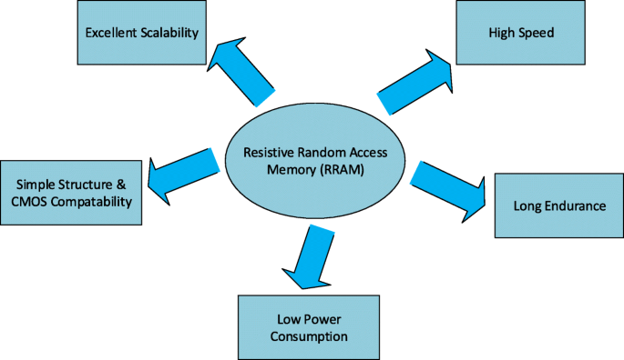
During the past several years, research in the field of emerging memory technologies has grown significantly and several prototype RRAM products have been developed demonstrating the potential for high-speed and low-power embedded memory applications. RRAM is one of the most promising memory technologies because of the advantages of simple structure, compatibility with the existing CMOS technology, good switching speed and ability to scale to the smallest dimensions. As a matter of fact, currently the Flash memory technology is facing difficulties to reduce to lower dimensions and as such RRAM is emerging as a potential replacement especially for fast operation and medium size storage density memory applications.
One of the most critical aspects that needs to be thoroughly investigated is that of the reliability of RRAM. A mechanism must be developed to ensure the detection of the operation failure of the device. Also designing circuits, e.g. a test element group (TEG) design for robust signal sensing, is one of the critical challenges for the emergence of RRAM devices. To achieve high-density memory operation in RRAM, the 1D1R operation is essential. This can be realized by operating the RRAM device in the unipolar mode. However, in the unipolar operation, higher current is needed for the reset process as compared to that of the bipolar operation. This is due to the fact that thermal effect plays a significant role in the unipolar reset process. Thus, to realize a high-density 1D1R RRAM array, the thermal effects both inside and outside a memory element needs to be considered. Also note that till date, in a single RRAM device, no technology has simultaneously reported fast switching, low power, and stable operation. Although, the endurance of RRAM has been reported as high as 10
12
[59], it is still not enough to be able to replace DRAM. The RRAM possesses the switching speed fast enough for DRAM replacement and the materials used in the fabrication for RRAM are very similar to that of DRAM, it becomes a critical challenge to improve the endurance characteristics of RRAM. To improve the endurance characteristics, it is necessary to control the oxygen movement between the electrode and the oxide layer at the interface. It is suggested to insert the second metal layer at the interface which can be easily oxidized and acts as an oxygen reservoir to prevent oxygen from penetrating into the electrode during the resistance switching. The most critical challenge hindering RRAM development till date is the proper understanding of the device switching mechanism which is since long being debated by researchers across the globe. The inconsistent switching mechanism of various reported RRAM devices is believed to be because of variation in the fabrication process, and thus, more rigorous analysis is needed in the future for obtaining a better understanding of the switching mechanism of RRAM devices. The aforesaid issues need to be handled effectively before implementing RRAM in future memory applications. Although, RRAM is highly attractive for use in neuromorphic computations, the biggest challenge to industrialize RRAM lies in its ability to tackle the variability issues, not only at nominal operating conditions but also at high temperatures before they can be used in a wide variety of applications.
Conclusion
This review article provides a brief introduction into the advancement of the memory architecture, the current trends and the limitations while providing a valuable insight into the field of emerging memory technologies. A detailed discussion, highlighting the importance of RRAM, its structure, working mechanism, and classification, has been presented. The key performance parameters and their effect on the RRAM operation has also been detailed within the current manuscript. An elaborate study on the MLC capability of RRAM, along with the methodology have been presented. The manuscript also discusses the important features of the widely accepted RRAM models. The implementation of RRAM for various important applications such as non-volatile logic, neuromorphic computing, security, and non-volatile SRAM have been highlighted. Although, significant success has been achieved in RRAM technology; however, more work is needed as RRAM still suffers from various challenges in terms in terms of high operation current, lower resistance ratios, and reliability issues. More efforts in research should aim to develop methods to achieve faster programming/erasing, lower power consumption, enhancing the storage density by implementing multilevel storage capability and improvement in the fabrication process for enhanced uniformity. In addition, renewed focus should be towards use of RRAM in embedded memory and non-volatile logic applications as breakthroughs in these fields are much more exciting and significant. With continued work and improvements, it is imperative that RRAM devices will be a standout technology for future non-volatile memory applications.
데이터 및 자료의 가용성
Not applicable.
약어
- RRAM:
-
Resistive random access memory
- MLC:
-
Multilevel cell
- RTN:
-
Random telegraph noise
- DRAM:
-
Dynamic random access memory
- SRAM:
-
Static random access memory
- PCM:
-
Phase change memory
- STT-MRAM:
-
Spin-transfer torque resistive random access memory
- LRS:
-
Low resistance state
- HRS:
-
High resistance state
- MTJ:
-
Magnetic tunneling junction
- MIM:
-
금속 절연체 금속
- MoM:
-
Metal-oxide-metal
- PLD:
-
Pulse laser deposition
- ALD:
-
원자층 증착
- V set :
-
Set voltage
- V reset :
-
Reset voltage
- V f :
-
Forming voltage
- I CC :
-
Compliance current
- CBRRAM:
-
Conductive bridge resistive random access memory
- OxRRAM:
-
Oxygen vacancies resistive random access memory
- ECM:
-
Electrochemical metallization memory
- VCM:
-
Valence change memory
- CF:
-
Conductive filament
- BE:
-
Bottom electrode
- TEM:
-
투과전자현미경
- I-V:
-
전류-전압
- 1T-1R:
-
1-Transistor 1-RRAM
- ANN:
-
Artificial neural network
- STDP:
-
Spike-time-dependent plasticity
- SRDP:
-
Spike-rate-dependent plasticity
- PUF:
-
Physical unclonable function
- CRP:
-
Challenge-response-pair
- nvSRAM:
-
Non-volatile SRAM
- TCAM:
-
Ternary content addressable memory
- TEG:
-
Test element group