여기에서 우리는 낮은 전류 밀도에서 질화물 마이크로 발광 다이오드(micro-LED)의 작동 동작 및 물리적 메커니즘에 대한 포괄적인 수치 연구를 보고합니다. 편광 효과에 대한 분석은 마이크로 LED가 낮은 전류 밀도에서 더 심각한 양자 구속 스타크 효과를 겪는다는 것을 보여주며, 이는 효율성을 개선하고 안정적인 풀 컬러 방출을 실현하는 데 어려움을 일으키고 있습니다. 최적의 작동 조건을 결정하고 낮은 전류 밀도에서 마이크로 LED의 구조 설계를 최적화하기 위해 캐리어 전송 및 매칭을 분석합니다. 활성 영역의 양자 우물 수가 적을수록 캐리어 정합 및 복사 재결합 속도가 향상되어 양자 효율 및 출력 전력이 향상되는 것으로 나타났습니다. 마이크로 LED에 대한 전자 차단층(EBL)의 효율성에 대해 논의합니다. EBL을 제거함으로써 전자 가둠과 정공 주입이 동시에 개선되는 것으로 밝혀졌으며, 따라서 마이크로 LED의 방출은 낮은 전류 밀도에서 크게 향상됩니다. Auger와 Shockley-Read-Hall에 대한 재조합 과정을 조사하고, 낮은 전류 밀도에서 마이크로 LED에 대한 결함에 대한 민감도를 강조합니다.
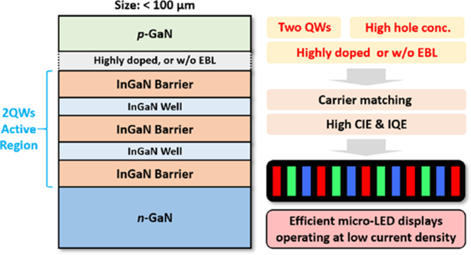
시놉시스 :저전류밀도에서 동작하는 InGaN 마이크로 LED의 분극유도 QCSE, 캐리어 수송 및 정합, 재결합 과정을 수치적으로 조사한다. 이러한 장치 거동과 메커니즘에 대한 이해를 바탕으로 효율적인 마이크로 LED 발광 디스플레이를 위해 고농도로 도핑되거나 EBL이 없는 두 개의 QW와 홀 농도가 높은 p-GaN을 포함하여 특별히 설계된 에피택셜 구조가 제안됩니다. 결함 밀도에 대한 감도는 마이크로 LED에서도 강조 표시됩니다.
<그림>
소개
III족 질화물 기반 가시광 발광 다이오드(LED)는 신호, 광통신, 정보 저장, 백라이트, 디스플레이 및 일반 조명(또는 고체 조명)을 포함한 광범위한 응용 분야를 가지고 있습니다[1, 2]. 2000년 Jiang과 그의 동료들에 의해 직경 12μm의 InGaN 마이크로 디스크 LED가 처음 시연된 이후[3, 4], 마이크로 LED는 고해상도 디스플레이 분야에서 학계 및 산업계의 관심을 확대하고 있습니다. , 가시 광선 통신, 생물 의학 및 감지 [5,6,7,8]. 마이크로 LED는 액정표시장치(LCD) 및 유기발광다이오드(OLED)에 비해 소형, 고해상도, 고광도, 고휘도, 고색채도, 긴 동작수명, 높은 응답속도, 및 견고성으로 인해 차세대 디스플레이 기술의 가장 유망한 후보가 되었습니다[9, 10]. 마이크로 LED 디스플레이의 응용 시나리오에는 고급 TV(TV), 노트북, 핸드헬드 및 모바일 단말 장치, 가상 현실(VR), 증강 현실(AR), 투명 디스플레이 등이 포함됩니다. Yole의 추정에 따르면 마이크로 LED 디스플레이 시장은 2025년까지 3억 3천만 개에 이를 것입니다[11].
III족 질화물 LED, 특히 고체 조명의 기존 응용 분야에서는 가능한 한 높은 광 출력이 필요합니다[12]. 지난 30년 동안 고전력 응용 프로그램, 에피택셜 구조의 설계 및 최적화, 장치의 작동 거동 및 물리적 메커니즘 연구, 제조 기술 개선을 포함한 질화물 LED에 대한 현대적인 연구, 주로 대형 칩, 높은 작동 전류 밀도 및 높은 입출력 전력에 중점을 둡니다[12, 13]. 무엇보다도 질화물 LED의 활성 영역은 초기 단계의 가장 단순한 이종 구조와 단일 양자 우물(QW)에서 5주기 QW를 갖는 오늘날의 다중 양자 우물(MQW)로 진화했으며 QW 수는 몇 가지 기간 동안 8 또는 10에 도달할 수도 있습니다. 상용화된 고전력 장치[14,15,16,17]. EBL은 특정 수준에서 정공 주입을 방해할 수 있다 하더라도 높은 주입 전류 밀도에서 전자 누출을 차단하기 위해 제안되었습니다[18, 19]. 기존의 고출력 LED의 경우 가장 실질적인 문제는 전류 밀도가 증가함에 따라 외부 양자 효율(EQE)이 감소하는 것으로, 이를 효율 드룹(efficiency droop)이라고 합니다. 이 거동의 고유 메커니즘은 주입된 캐리어 밀도가 높을 때 간접 오제 재결합과 관련이 있습니다[20]. 제조와 관련하여 박막 플립칩 및 수직 주입 기하학이 개발되어 질화물 LED의 전력 수준을 확장합니다[21, 22].
기존의 대형 고출력 질화물 LED에 대해 상당한 발전이 있었으며, 배운 교훈 중 일부는 마이크로 LED 연구에 활용할 수 있습니다. 그러나 마이크로 LED는 여전히 고전력 제품과 크게 다릅니다. 마이크로 LED의 다양한 작동 동작, 메커니즘 및 조건은 다른 도전과 연구 경로를 초래할 수 있습니다[23, 24]. 기존 LED의 경우 피크 EQE는 높은 전류 밀도에 위치하며 작동 전류 밀도는 피크 효율(> 30A cm
−2
이상)에 있습니다. ). 그러나 마이크로 LED 발광형 디스플레이의 경우 작동 전류 밀도는 훨씬 낮아야 하며 종종 0.02 ~ 2A cm
−2
범위에 있어야 합니다. [24]. 이 낮은 전류 밀도에서 기존 질화물 LED의 EQE는 매우 낮고 실용적인 마이크로 LED 디스플레이 애플리케이션에 충분하지 않습니다. V-pit의 이점을 활용하여 전위를 차단하고 정공 주입을 향상함으로써 Zhang과 그의 동료들은 0.8A/cm2에서 최대 효율이 24.0%인 효율적인 InGaN 기반 LED를 만들었습니다.
2
. 그러나 Zhang et al.에 의해 보고된 LED 칩. 여전히 기존 크기(1mm × 1mm)로 제한되며, 이는 마이크로 LED보다 훨씬 더 큽니다[25]. 또한, 마이크로 LED의 내부 양자 효율(IQE) 및 EQE는 칩 크기가 감소함에 따라 감소한다는 많은 연구가 보고되었다[26,27,28]. 이 크기 의존적 열화는 주로 표면 재결합 및 플라즈마 보조 건식 에칭에 의해 유도된 측벽 손상에 기인합니다. 이러한 측벽 효과는 SRH(Shockley-Read-Hall) 비방사성 재결합에 기여한 다음 양자 효율을 감소시키고 비표면적/측벽 면적이 크기 때문에 칩 크기가 작을수록 심각해집니다. 장치의 활성 영역 [29,30,31]. 이 문제를 해결하기 위해 유전체 재료를 사용한 측벽 패시베이션과 완충 불산 또는 광전기화학적 방법을 사용한 습식 에칭이 마이크로 LED에 대해 이러한 영향을 일정 수준으로 최소화하는 것이 제안되었습니다[31,32,33]. 그러나 측벽 패시베이션으로 개선되더라도 마이크로 LED(60μm보다 작은 크기)의 피크 EQE는 여전히 25%보다 낮으며 2A cm보다 낮은 전류 밀도에서 몇 퍼센트로 급격히 감소합니다. −2
[34, 35]. 특히 InGaN 기반 적색 마이크로 LED의 경우 현재 보고된 EQE는 미니 디스플레이에 대한 강한 편광과 열악한 결정 품질(0.2%)로 인해 1% 미만으로 상당히 제한됩니다. Appl Phys Express 14:011004" href="/articles/10.1186/s11671-021-03557-4#ref-CR36" id="ref-link-section-d295113462e757">36]. 또한, 칩 크기가 줄어들면서 피크 EQE의 위치도 더 높은 전류 밀도로 이동하여 낮은 전류 밀도에서 고효율을 더욱 저해합니다[26].
따라서 낮은 전류 밀도에서 양자 효율을 개선하는 것은 마이크로 LED 발광 디스플레이 응용 분야에서 큰 도전이자 중요한 과학적 문제가 됩니다. 이를 위해 피크 효율을 높이고 효율의 시작 위치를 적절한 낮은 전류 밀도로 이동해야 합니다. 이전에는 주로 측벽 패시베이션과 같은 제조 기술의 개선에 중점을 두었습니다. 효율성을 높이려면 아직 상대적으로 탐구되지 않고 이해가 부족한 저전류 밀도에서 마이크로 LED의 작동 동작과 물리적 메커니즘을 조사하는 것도 필수적입니다. 또한, 저전류밀도에서 최대값으로 효율을 향상시킬 수 있는 소자를 만들기 위해서는 마이크로 LED의 에피택시 구조도 재설계하고 최적화해야 하는데, 이는 기존의 대형 고출력 소자와 상당히 달라야 한다. 입출력 대응. 현재로서는 낮은 전류 밀도에서 작동하는 마이크로 LED 발광형 디스플레이를 위해 특별히 설계된 에피택시 구조가 부족합니다.
이 연구에서는 낮은 전류 밀도에서 작동하는 디스플레이 애플리케이션을 위한 마이크로 LED의 고유한 과제를 강조하고 이를 해결하기 위한 잠재적인 솔루션을 제안합니다. 소프트웨어 Advanced Physical Model of Semiconductor Devices[37]를 사용하여 200~0.1A/cm
2
다양한 전류 밀도에서 InGaN 마이크로 LED의 작동 동작과 물리적 메커니즘을 수치적으로 조사합니다. . 마이크로 LED의 QCSE를 위해 band diagram, wavefunction, polarization field를 모의하여 분석하였으며, 낮은 전류밀도에서 더 심한 QCSE를 확인하였다. QW 수의 영향, p 마이크로 LED의 캐리어 수송, 캐리어 정합, 복사 재결합 및 양자 효율에 대한 형 도핑 농도 및 AlGaN EBL을 체계적으로 조사합니다. SRH 및 Auger 재조합에 관한 효과 및 메커니즘도 논의됩니다. 시뮬레이션 및 분석을 기반으로 낮은 전류 밀도에서 작동하는 마이크로 LED를 위해 특별히 설계된 최적화된 에피택시 구조를 제안합니다.
장치 구조 및 시뮬레이션 방법
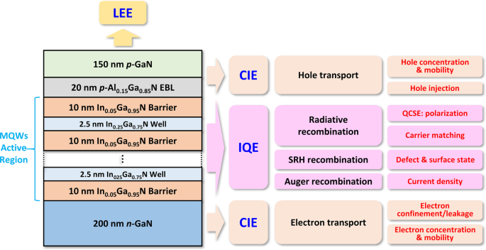
이 연구에서는 60 × 60μm의 직사각형 칩 크기와 465nm 부근의 피크 방출 파장을 갖는 청색 InGaN 마이크로 LED의 공통 구조가 시뮬레이션에 사용됩니다. 그림 1은 파란색 마이크로 LED가 200nm n -GaN 층, MQW 활성 영역, 20nm p -알0.15 Ga0.85 N EBL 및 150nm p -GaN 층. MQW 활성 영역은 2.5nm 두께의 In0.25가 있는 8, 5, 3, 2 또는 1 주기로 구성됩니다. Ga0.75 10nm 두께의 In0.05에 내장된 N QW Ga0.95 N 양자 장벽(QB). MQW의 In 구성은 원하는 청색 방출 파장을 달성하도록 조정 및 최적화됩니다. n의 도핑 농도 -GaN, p -AlGaN EBL 및 p -GaN은 2 × 10
18
입니다. cm
−3
, 3 × 10
18
cm
−3
및 1 × 10
19
cm
−3
, 각각.
<사진>
시뮬레이션 및 LED 효율 분석에 사용된 InGaN/GaN 기반 청색 발광 다이오드의 개략도
마이크로 LED의 광학 및 전기적 특성은 소프트웨어 Advanced Physical Model of Semiconductor Devices [37]를 사용하여 수치적으로 조사됩니다. 시뮬레이션에서는 자발 분극과 압전 분극으로 인한 계면 전하 밀도의 50%를 가정합니다[38]. 특별히 언급된 것을 제외하고 SRH 수명 및 Auger 재결합 계수는 100ns 및 1 × 10
–31
로 설정됩니다. cm
6
s
−1
, 각각 [39, 40]. 대역 오프셋 비율은 0.7/0.3으로 가정하고 [41], 광 추출 효율은 70%로 고정되며 작동 온도는 300K입니다. 시뮬레이션에 사용된 다른 재료 매개변수는 참조 [42]에서 찾을 수 있습니다.
여기서 R라드 복사 재결합 속도, RSRH 는 SRH 비방사성 재결합율이며, R오거 는 Auger 재조합 속도입니다. 그림 1은 다양한 종류의 효율성과 관련 물리적 메커니즘 및 요인을 보여줍니다.
R라드 및 CIE는 최대화되어야 하고, 전기 효율과 LEE는 개선되어야 하고, SRH와 Auger 재결합은 낮은 전류 밀도에서 동작하는 마이크로 LED의 전체 효율을 개선하기 위해 감소되어야 한다. 이러한 모든 문제를 해결하려면 시스템 수준의 접근 방식이 필요합니다. 광 추출을 제외하고 이러한 문제는 다음 섹션에서 논의될 것이며 마이크로 LED의 효율적인 에피택셜 구조를 만들기 위한 잠재적 솔루션도 제안될 것입니다.
저전류 밀도에서의 QCSE:내부 분극장
편광 유도 QCSE는 질화물 LED의 IQE를 제한하는 지배적인 요인 중 하나입니다[44]. QCSE는 기존의 대형 고출력 LED에 대해 널리 연구되었지만 여전히 마이크로 LED 특정 응용 프로그램의 맥락에서 충분한 논의가 부족합니다. 따라서 이 중요한 효과를 먼저 조사합니다. 여기서 논의된 마이크로 LED의 활성 영역은 5주기 QW로 구성되며, 이는 기존의 질화물 LED에 가장 일반적으로 사용되는 QW 수입니다.
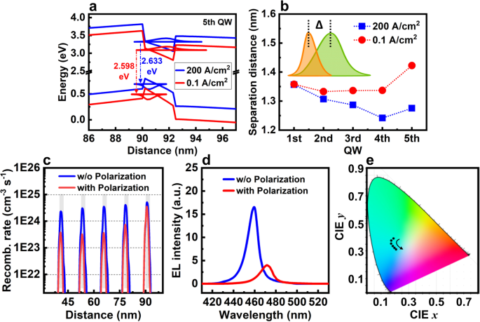
그림 2a는 200 및 0.1 A/cm
2
에서 다섯 번째 QW의 에너지 밴드 다이어그램과 관련 1차 전자 및 정공 파동 함수를 보여줍니다. . QB와 QW는 큰 밴드 굽힘을 경험하여 전자와 정공 파동 함수의 공간적 분리로 이어집니다. 또한 밴드 벤딩은 낮은 전류 밀도에서 더 강해 QCSE가 더 강함을 나타냅니다. 이 현상은 낮은 주입 전류 밀도에서 더 적은 비평형 캐리어가 있는 약한 스크리닝 효과에 기인합니다(추가 파일 1:그림 S1a-d 및 관련 논의 참조)[41]. 그림 2b는 더 심한 QCSE가 낮은 전류 밀도에서 반송파 함수의 공간적 분리를 향상시켜 더 낮은 복사 재결합 속도를 초래한다는 것을 보여줍니다. 복사 재결합 속도와 편광 효과가 있거나 없는, 즉 QCSE가 있는 경우와 없는 경우, 전자-정공 분리가 낮은 전류 밀도에서 방출을 정량적으로 감소시키는 방법을 보여주기 위해 추가로 계산됩니다. 그림 2c, d는 복사 재결합 속도의 적분 강도와 EL 강도가 QCSE에 의해 각각 약 84.0% 및 72.3% 감소되었음을 보여줍니다. 이러한 결과는 낮은 전류 밀도에서 향상된 QCSE로 인해 기존의 고전력 조합보다 마이크로 LED의 효율을 개선하기가 더 어렵다는 것을 나타냅니다.
<그림>
아 200 및 0.1A/cm
2
에서 다섯 번째 QW의 에너지 밴드 다이어그램 및 관련 1차 전자 및 정공 파동 함수 , 각각. ㄴ 200 및 0.1 A/cm
2
에서 전자 및 정공 파동 함수의 피크 위치 분리 거리 , 각각. ㄷ 방사성 재결합 속도 및 d 0.1A/cm
2
에서 계산된 EL 스펙트럼 극성이 없는 것과 없는 것. 이 전류 밀도가 0.1~20A/cm
2
인 파란색, 녹색 및 빨간색 LED에서 생성된 색점 1931-CIE(x, y) 색도 다이어그램에 표시됨
또한 다양한 주입 전류 밀도에서 방출 파장의 정확하고 안정적인 제어는 밝기, 색상 정확도 및 채도와 같은 다양한 중요한 매개변수를 결정하기 때문에 마이크로 LED 디스플레이에 매우 중요합니다. 그러나 낮은 전류 밀도에서 더 심한 QCSE는 특히 더 높은 인듐 조성을 필요로 하는 녹색 및 적색 마이크로 LED의 경우 이를 큰 과제로 만듭니다. 더 높은 인듐 조성과 더 강한 QCSE를 가진 InGaN QW에서 밴드 굽힘이 증가된 직접적인 결과로, 스크리닝 효과로 인해 전류 밀도에 대한 파장 이동이 더 뚜렷해집니다. 다양한 전류 밀도를 갖는 InGaN 기반 적색, 녹색 및 청색 마이크로 LED의 EL 스펙트럼은 스펙트럼 이동이 디스플레이의 색점에 어떻게 영향을 미치는지 보여주기 위해 추가로 계산됩니다. 추가 파일 1:그림 S2는 0.1 ~ 20A/cm
2
, 피크 파장 청색은 적색, 녹색 및 청색 마이크로 LED에 대해 각각 약 15.8, 6.6 및 1.7nm만큼 이동합니다. 추가 파일 1:표 S1에 요약된 대로 빨간색, 녹색 및 파란색 마이크로 LED를 결합하여 생성된 색상 포인트도 계산됩니다. 그림 2e는 해당 1931-CIE(x, y) 색도 다이어그램을 보여줍니다. 분명히 RGB 마이크로 LED의 방출 색상은 전류 밀도가 증가할 때 녹색에서 청록색으로 크게 변경되었습니다. 1931-CIE x 값은 0.1676에서 0.2084로 교차하고 1931-CIE y 값은 0.3891에서 0.3106으로 교차합니다. 이러한 색상 포인트 대 전류 밀도의 실질적인 변화는 마이크로 LED 디스플레이의 성능을 크게 저하시킵니다.
많은 보고서에서 InGaN/AlGaN 초박형 초격자 장벽[45], GaN 층간 장벽이 있는 InGaN/GaN/AlGaN/GaN MQW[46], 주름진 MQW[47], MQW 이전의 스트레인 릴리프 레이어 [48]. 그러나 QCSE는 c의 고유한 속성에 의해 유도됩니다. -평면 질화물 재료. MQW를 여러 번 조정하는 것만으로는 이 효과를 완전히 억제할 수 없습니다. 최근 무극성 질화물 LED에 대해 상당한 효율이 달성되었다. 비극성 GaN 기판의 비용을 줄일 수 있다면 비극성 LED는 QCSE를 줄이고 안정적인 풀 컬러 방출을 실현하는 이상적인 솔루션이 될 수 있습니다[49].
여기서 σn 및 σp 전도도를 나타냅니다. n 그리고 p 농도, μn 그리고 μp 는 각각 전자와 정공의 이동도이며 E 전기장을 나타냅니다. 질화물에서 정공 농도는 전자보다 10배 더 낮고[50], 정공 이동도는 전자보다 2배 더 낮습니다[51]. 이러한 농도와 이동성의 비대칭은 캐리어 플럭스(Jn> Jp ) 및 다음 두 가지 방법으로 LED의 성능을 저하시킵니다.
현재 분사 효율 :전류 주입 효율 ηCIE 재결합 전류 J의 비율을 나타냅니다. 재조합 총 현재 J총계 , 다음 등식 [52]:
여기서 C 상수, E이력서 전환 에너지, h 플랑크 상수, ν이력서 생성된 빛의 주파수, ρr 감소된 상태 밀도, <>f ㄷ 그리고 fv 페르미-디랙 분포, 그리고 |MT|
2
는 운동량 행렬 요소[53]입니다. QW에서 더 적은 정공과 추가 전자 축적은 결정 격자의 확장과 인장 변형의 축적으로 이어질 수 있습니다. 이 응력 변화 하에서 가전자대 최대값 주변의 양자 준위의 전하 밀도가 감소합니다. 이것은 광학 전이 확률을 더욱 감소시키고 R을 감소시킵니다. 라드 식에 따라 (7). 이러한 방식으로 단일 QW에서 로컬 캐리어 불일치도 IQE를 제한합니다. 이 주제에 대한 보다 구체적인 논의는 이전 보고서[54,55,56]에서 찾을 수 있습니다.
다음 섹션에서는 QW 번호, p의 영향 -유형 도핑 농도 및 캐리어 전송의 EBL 구조를 분석하여 최상의 캐리어 매칭 조건을 결정합니다. 마지막으로 낮은 전류 밀도에서 작동하는 효율적인 마이크로 LED 디스플레이를 위한 최적화된 에피택시 구조를 제안합니다.
5QW의 캐리어 불일치
먼저, 5QW를 갖는 청색 마이크로 LED의 캐리어 수송 특성을 시뮬레이션합니다. 200A/cm
2
에서의 캐리어 농도 분포 및 0.1A/cm
2
추가 파일 1:그림 S3a 및 b에 각각 설명되어 있습니다. 5 QW의 불균일한 분포는 높은 전류 밀도와 낮은 전류 밀도에서 모두 관찰할 수 있습니다. 추가 파일 1:그림 S3c 및 d는 MQW(684cm
2
V
−1
s
−1
)는 구멍 이동도(10cm
2
)보다 2배 더 높습니다. V
−1
s
−1
). 따라서 전자는 재결합에 참여하지 않고 MQW에 주입한 다음 통과하여 전자 누출 문제와 낮은 CIE를 유발할 수 있습니다[51].
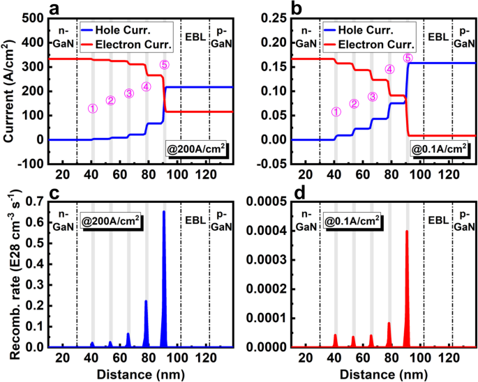
그림 3a는 200A/cm
2
에서 전자 및 정공 전류 밀도의 분포를 보여줍니다. . 총 구멍 전류 밀도(217.4A/cm
2
)은 전자의 65.2%에 불과합니다(333.3 A/cm
2
). ), 캐리어와 낮은 CIE의 심각한 불일치를 나타냅니다. 누설 전자 전류는 116.0A/cm
2
만큼 높습니다. , 이는 복사 효율과 정공 주입 모두를 저하시킵니다. 도 3b에 도시된 바와 같이 누설 전자 전류는 0.01A/cm
2
에 불과하다. , 계산된 ηCIE 0.1A/cm
2
에서 최대 95% . 이러한 결과는 낮은 전류 밀도에서 높은 CIE를 달성하는 것이 더 쉽다는 것을 나타냅니다. 그러나 J인 5번째 QW를 제외하고 pJ와 같을 수 있습니다. n , 캐리어 불일치 및 추가 전자 축적은 높은 전류 밀도와 낮은 전류 밀도 모두에서 다른 4개의 QW(QW 1, 2, 3 및 4)에서 상당히 심각합니다. 200A/cm
2
에서 , 이 4개의 QW의 전자 전류 밀도는 정공 전류 밀도보다 120, 43, 16 및 5배 더 높습니다(그림 3a). 0.1A/cm
2
에서 , 그들은 정공 전류보다 23, 9, 4 및 2배 더 높습니다(그림 3b). 식을 기반으로 합니다. (7), 이 큰 캐리어 불일치는 이 4개의 QW의 복사 재결합 속도를 분명히 감소시킵니다. 따라서 이 4개의 QW에서 복사 재결합 비율은 200A/cm2에서 약 3.4%, 4.0%, 10.1% 및 34.2%입니다.
2
및 0.1A/cm
2
에서 11.3%, 10.1%, 10.7% 및 21.2% 5QW에 비해 이러한 캐리어 불일치 및 낮은 복사 방출은 마침내 마이크로 LED의 모놀리식 효율을 감소시킵니다.
<그림>
5QW a가 있는 LED의 캐리어 전류 분포 200A/cm
2
에서 그리고 b 0.1A/cm
2
에서 . 5QW c가 있는 LED의 복사 재결합 속도 200A/cm
2
에서 그리고 d 0.1A/cm
2
에서
캐리어 전송 및 매칭에 영향을 미치는 요소
QW 번호 :고전류 밀도에서 작동하는 기존의 대형 LED의 경우 높은 광 출력 전력을 달성하려면 5, 8 또는 10주기의 MQW를 사용해야 합니다. 그러나 마이크로 LED 발광형 디스플레이의 경우 출력 전력이 훨씬 작고 작동 전류 밀도가 훨씬 낮습니다. 이전 섹션에서 논의한 바와 같이 낮은 전류 밀도에서도 5QW에서 캐리어 부정합이 상당히 심각하게 남아 있으며 하나의 QW만이 최상의 정합 조건을 달성할 수 있습니다. 이러한 관점에서 볼 때 낮은 전류 밀도에서 작동하는 마이크로 LED의 경우 QW 수가 적은 활성 영역이 개선된 캐리어 정합으로 인한 효율성 향상을 위해 더 나은 설계가 되어야 합니다.
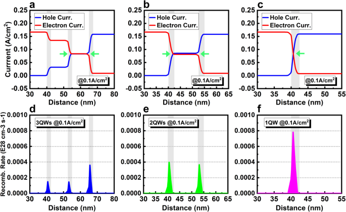
마이크로 LED에 대한 QW 수의 영향은 우리의 가정을 검증하기 위해 조사되었습니다. 그림 4a–f는 0.1A/cm
2
에서 캐리어 전류 밀도와 복사 재결합 속도를 보여줍니다. 각각 3QW, 2QW 및 1QW의 LED입니다. 현재 곡선에는 단 하나의 교차점이 있습니다(가장 좋은 캐리어 일치의 한 점, Jn =Jp ) 전류의 단조 감소 경향으로 인해 3QW 및 2QW의 경우와 같이 QW가 더 적을수록 두 개의 다른 QW에서 두 개의 교차점이 달성될 수 있습니다(그림 4a, b). 즉, MQW의 캐리어 불일치는 더 적은 QW로 부분적으로 극복될 수 있습니다. 특히 2QW의 경우 적절한 조정을 통해 두 QW 모두에서 캐리어 플럭스의 완벽한 일치를 달성할 수 있습니다. 복사 재결합에 의한 캐리어 소비는 QW가 적은 활성 영역에 더 집중되기 때문에 복사 재결합 비율은 3QW 및 5QW보다 2QW에서도 더 높습니다(그림 3d, 4d, e). 의심할 여지 없이 최고의 캐리어 정합은 하나의 QW만 있는 LED에 있으며, 그림 4c, f에 표시된 것처럼 복사 재결합 비율도 1QW에 대해 가장 높습니다.
<그림>
a가 있는 LED의 캐리어 전류 분포 3QW, b 2QW 및 c 0.1A/cm에서 1QW
2
. d를 사용한 LED의 복사 재결합 비율 3QW, e 2QW 및 f 0.1A/cm에서 1QW
2
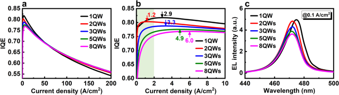
그림 5a, b는 0 ~ 200A/cm
2
전류 밀도의 함수로 IQE를 보여줍니다. 및 0 ~ 10A/cm
2
, 각각. 50A/cm
2
보다 높은 전류 밀도의 경우 , QW 수가 감소하면 IQE가 감소합니다. 대조적으로, 전류 밀도가 약 30A/cm
2
미만인 IQE는 QW 수가 감소하면 증가합니다. 0.1A/cm
2
에서 , 8, 5, 3, 2 및 1 QW에 대한 IQE 값은 각각 55%, 62%, 69%, 77% 및 78%입니다. 또한, Fig. 5b와 같이 피크 IQE의 위치도 6.0 A/cm
2
에서 이동한다. 8 QW에서 가장 낮은 전류 밀도 약 1.2A/cm
2
2QW에서. 낮은 전류 밀도(<1 A/cm
2
)에서 IQE 곡선 ) 또한 QW 수치가 낮을수록 더 가파르고 날카로워지며, 이는 최고 효율을 달성하는 것이 더 쉽고 빠르다는 것을 나타냅니다. 이는 낮은 전류 밀도에서 효율성을 향상시키는 데 매우 유용합니다. 이러한 IQE 경향 뒤에 있는 물리적 메커니즘은 캐리어 플럭스의 더 나은 일치와 더 적은 QW 번호로 활성 영역에서 더 집중되고 더 강한 복사 방출로 설명될 수 있습니다. 도 5c에 도시된 바와 같이, 8 QW와 비교하여, 0.1 A/cm
2
에서 5, 3, 2 및 1 QW의 적분 EL 강도 각각 약 6.1%, 14.8%, 28.4%, 32.1% 증가했습니다. 이 결과는 더 적은 QW number로 효율뿐만 아니라 출력도 향상되었음을 확인시켜준다.
<그림>
아 IQE 곡선 및 b IQE는 8, 5, 3, 2 및 1 QW의 LED의 낮은 전류 밀도에서 곡선을 이룹니다. ㄷ 0.1A/cm
2
에서 8, 5, 3, 2 및 1 QW가 있는 LED의 EL 스펙트럼
시뮬레이션 결과는 1QW가 가장 높은 EL 강도를 가지며 낮은 전류 밀도에서 작동하는 마이크로 LED에 가장 적합한 구조일 수 있음을 보여줍니다. 그러나 실험적으로 평평한 표면과 날카로운 계면을 갖는 하나의 QW만을 에피택셜 성장시키는 것은 어렵다. 또한 1QW 구조의 경우 피크 IQE의 위치가 2.9A/cm2로 약간 증가합니다.
2
, IQE 곡선의 모양도 약간 변경되었습니다. 이는 단일 QW의 특수한 상황으로 설명할 수 있다. 다른 QW에 비해 EBL에 인접한 QW는 특수한 분극 환경을 갖고 있어 '문제 QW'로 간주된다. 이 주제는 AlGaN EBL 섹션에서 더 자세히 논의될 것입니다. . 이러한 이유를 고려할 때, 2QW는 캐리어 플럭스, 가까운 IQE 값 및 1QW에 대한 EL 강도의 유사한 양호한 매칭을 갖는 최상의 활성 영역 디자인이어야 합니다. 따라서 다음 섹션에서 모든 시뮬레이션은 2QW가 있는 마이크로 LED를 기반으로 합니다.
P-GaN 도핑 농도 :p가 다른 2QW LED의 성능 - p의 유형 도핑 농도 -GaN은 추가로 조사됩니다. 도 6a에 도시된 바와 같이, p의 도핑 농도가 -1 × 10
18
에서 증가하는 GaN cm
−3
~ 5 × 10
19
cm
−3
, 0.1A/cm
2
에서의 복사 재결합 속도 두 QW에 대해 약 3.1% 및 3.0% 추가로 증가합니다. 그림 6b는 총 정공 전류 밀도가 0.157에서 0.162A/cm
2
로 증가함을 보여줍니다. 한편, 누설 전자 전류 밀도는 0.009에서 0.005A/cm
2
로 감소합니다. 도핑 농도의 증가와 함께. n 근처의 QW에서 재결합 전류가 -side가 p 근처의 QW보다 높습니다. -측면(그림 6b). 따라서 n 부근의 복사재결합율은 -side QW도 p 근처보다 약간 높습니다. -사이드 QW. As shown in Fig. 6c, one can find that the energy barrier for carriers in EBL, which is defined as the energy distance between the electron/hole quasi-Fermi level and the highest conduction band or lowest valence band, are almost unchanged under differnt doping concentration of p -GaN, that is, the hole injection is not improved by increasing doping concentration. Figure 6d shows the average hole concentration in the p -GaN and QWs. The hole concentration in the p -GaN is almost exponentially dependent on the doping concentration. Inside the QWs, the hole concentration is increased approximately twice from 1.59 × 10
19
cm
−3
to 3.08 × 10
19
cm
−3
with a higher doping concentration. These results indicate that the increased hole concentration is the main contribution for the improvement of radiative recombination. Therefore, even at low current density, the p -type doping problem of nitride remains notable, and enhancing the doping efficiency and hole concentration is still beneficial for the efficiency of micro-LED.
아 Radiative recombination rates of 2QWs LED with various doping concentrations in p-GaN. ㄴ Carrier current distribution with different doping concentrations in p -GaN. ㄷ Enlarged energy band diagrams of EBL with different doping concentrations in p -GaN. d Average hole concentration in p -GaN and QWs with various doping concentrations of p -GaN
AlGaN EBL :In the last decades, a 10–20 nm p -type AlGaN EBL has become a standard structure for traditional nitride-based LEDs. This EBL is considered to block the electron leakage and suppress the efficiency droop under high injected current density. In spite of this, it is worth noting that the EBL is still a very complicated, subtle structure for the LED. It involves many important factors, including Al composition, p -type doping efficiency of AlGaN, band offset ratios, and polarization effect. Each of them can influence the band structure and carrier transport substantially, then determines the effectiveness of EBL. For the construction of EBL, thickness, composition, and doping concentration must be considered and optimized carefully to balance the enhancement of electron confinement and the blocking of hole injection, otherwise, the opposite may happen, and the performance of LED might deteriorate. For micro-LED, the effectiveness of EBL for operating at low current density must be reconsidered, which may be different with the case of traditional high input/output LED.
a. Doping concentration of EBL :First, the effect of EBL doping concentration on carrier transport at low current density is investigated. The thickness and Al composition of EBL are fixed as 20 nm and 0.15, respectively. Considering the low solubility of Mg dopant in AlGaN, the crystal degradation, and compensation effect by over-doping [50], the doping concentration of EBL is first set as be 3 × 10
18
cm
−3
. Figure 7a shows the corresponding energy band structure. Clearly, despite the existence of EBL, the electron leakage out of the QW still can be caused by the insufficient electron confinement due to the downward bending of the last QW and EBL. A new energy valley under the electron quasi-Fermi level appears at the interface of last QB and EBL. Thus, electrons would escape from QW and accumulate in this area. This distortion of band structure makes the EBL relatively ineffective, and it can be contributed to the polarization effect. As shown in Fig. 7c, the strong polarization induces a large amount of charges at the interfaces. Due to the unbalanced polarization charges are positive at the interface of the last QB/EBL, a large electrostatic field pointing from the p -side to the n -side builds up in the last QB, which is opposite to the fields in other QBs and EBL. These electrostatic fields pull down the energy band of the last QB and EBL. Moreover, the electric fields in the last QW and last QB both can attract electrons and drive them out of the active region into the p -layer. This can be observed in the carrier concentration diagram, as shown in Fig. 7d. The dotted black line indicates that a part of the electrons escape from the active region and accumulate at the interface of last QB/EBL. In the EBL and p -GaN, the leakage electron remains relatively high.
Energy band diagrams of 2QWs LED with a 3 × 10
18
cm
−3
그리고 b 6 × 10
19
cm
−3
doping concentration in AlGaN EBL. ㄷ Space charge density and d carrier concentration distribution of 2QWs LED with 3 × 10
18
and 6 × 10
19
cm
−3
doping concentration of EBL. The inset of c shows the direction of polarization fields
On the other hand, the EBL also introduces a potential barrier as high as 480 meV for hole injection. Moreover, as shown in Fig. 7a, c, an energy valley close to the hole quasi-Fermi level appears at the interface region between the EBL/p -GaN due to the polarization effect. As indicated by the solid black line of Fig. 7d, most of the holes are blocked by the EBL and thus, accumulate at the energy valley of the EBL/p -GaN interface. Owing to this inefficient carrier transport, the last QW is considered as a “problem QW,” and the EBL only has a low capability for electron confinement, and should be responsible for the poor hole injection. Compared with the traditional high input/output LED, this polarization induced ineffectiveness of the EBL function could be particularly severe for the micro-LED due to the enhanced polarization effect by less carrier screening at low current density.
Band engineering by increasing the doping concentration of EBL is a possible method to improve the electron confinement and hole injection. The activation energy of Mg dopant in AlGaN EBL is higher than GaN, therefore, even under a similar doping concentration, the active hole concentration in EBL remains much lower than p -GaN. The lower hole concentration could further separate the hole quasi-Fermi level and valence band, then increase barrier height. Based on this analysis, the doping concentration of EBL needs to be much higher than p -GaN. Considering the doping limitation in actual experiment, 6 × 10
19
cm
−3
is selected as a new doping concentration in the EBL. As shown in Fig. 7b, by increasing the doping concentration, the valence band of EBL is lifted due to the alignment of hole quasi-Fermi level, resulting in a reduced hole energy barrier of 281 meV. Moreover, the high p -type doping also helps lower the electron quasi-Fermi level with respect to the conduction band in EBL, hence increasing the effect barrier for electron leakage to 1175 meV. These changes improve electron confinement and hole injection. Figure 7d shows that compared with the doping concentration of 3 × 10
18
cm
−3
, the hole concentration in the active region is greatly increased, and the leakage electron in the EBL and p -GaN is reduced to almost zero. However, the energy valley at the interface between the EBL/p -GaN still exists. Moreover, the upward of valence band also introduces a new energy valley for the hole accumulation at the interface between the last QB/EBL, which can be confirmed by the hole concentration distribution in Fig. 7d. These energy valleys can impede the hole injection into QWs, hence compensating the advantage of high doping concentration.
b. Al composition of EBL :Compared with the increase of doping concentration, reducing the composition of AlGaN EBL may be an easier, more efficient method to improve the carrier transport at low current density. The effectiveness of EBL is sensitively dependent on Al composition, band offset, and polarization effect. Increasing the Al composition of EBL can increase the band offset between the last QB/EBL, which increases the electron barrier height. However, as shown in Fig. 8a, the polarization-induced charges at the interfaces also increase accordingly, which pull down the electron barrier height. Two mechanisms have the opposite effect for confining electrons.
아 Space charge density distribution of 2QWs LED with different EBL. The inset shows the direction of polarization field. Energy band diagrams of 2QWs LED b with Al0.1 Ga0.9 N EBL and c without EBL. d Carrier concentration distribution, e carrier current density, f IQE and g EL spectra of 2QWs LED with different EBL. The inset of g shows the working voltages at 0.1 and 1 A/cm
2
with different EBLs
Based on this analysis, the carrier transport of 2QWs micro-LEDs with different EBL structures at 200 and 0.1 A/cm
2
are investigated. The result of effective energy barrier heights of different EBL are summarized in Table 1. First of all, both the electron and hole energy barriers at low current density are much higher than the cases of at high current density due to the lower nonequilibrium carrier population. A higher energy barrier can improve the electron confinement, but also severely impedes the hole injection at low current density. This indicates that the influence of EBL on the carrier transport of micro-LED operating at low current density is much higher than that of the traditional high input/output LED. Table 1 also shows that with a relatively low Al composition in EBL, the electron barrier decreases with Al composition increased, which indicates that the downward of conduction band induced by polarization effect is larger than the increased band offset introduced by the higher Al composition. By further increasing the composition, the electron barrier increases along with composition, meaning that the band offset becomes dominant over the polarization effect. Compared with high current density, this turning point of composition is higher at low current density due to the enhanced polarization effect by less carrier screening. On the other hand, because of the original band offset between the last QB/p -GaN and the band bending, there are energy barriers for electron and holes exist at the interface even without the EBL. At 200 A/cm
2
, when the composition is lower than 0.20, the electron energy barrier is lower than the case of without EBL, but the hole barrier is higher approximately 64 meV. At 0.1 A/cm
2
, even with composition higher than 0.20, the electron barrier of AlGaN EBL (523 meV) is still 151 meV lower than the case of without EBL (674 meV), but the hole barrier is increased approximately 76 meV from 409 to 485 meV. These results indicate that both the electron confinement and hole injection could be deteriorated by the EBL with an incorrect composition, especially for micro-LED operating at low current density.
For a deep analysis, band structures of micro-LEDs with Al0.10 Ga0.90 N EBL and without EBL as representatives are illustrated in Fig. 8b, c. The EBL introduces two energy valleys at the interface of last QB/EBL and EBL/p -GaN for electron and hole accumulation, respectively, which can be confirmed by the carrier concentration diagram in Fig. 8d. Therefore, the electron confinement and hole injection are poor for this structure. When the EBL is removed, as shown in Fig. 8c, the energy barrier for electron is increased, and the energy valley for electron extracting and accumulation disappeares. These changes prevent electrons leakage more effectively, as confirmed in Fig. 8d. Meanwhile, the barrier height for hole injection is reduced, and the energy valley at the EBL/p-GaN interface is also removed. So, the hole can transport directly into the QW without facing large obstacle, as shown in Fig. 8c, d.
The above careful investigation suggests that without EBL may be a better structure for the micro-LED operating at low current density. Simulation results support our suggestion. Figure 8e illustrates the carrier current density at 0.1 A/cm
2
with different EBL structures. When the Al composition of the EBL is reduced from 0.15 to 0.04, the total electron and hole current densities increase from 0.167 and 0.159 A/cm
2
to 0.225 and 0.225 A/cm
2
, 각각. Moreover, when the EBL is completely removed, both the total electron and total hole current densities greatly increase to 0.528 A/cm
2
, which is approximately 3 times higher compared with the Al0.15 Ga0.85 N EBL. This enhancement is contributed to the improved electron confinement and hole injection.
Figure 8f shows the IQE curves at low current density. When the Al composition of EBL is reduced from 0.15 to 0.04, the IQE values increase evidently due to the improved carrier transport. However, by removing the EBL, the IQE value experiences a slight decrease compared with Al0.04 Ga0.96 N EBL. This can be explained by the carrier matching in two QWs. As indicated by the green arrows in Fig. 8e, a, perfect carrier matching occurred in both the two QWs with Al0.04 Ga0.96 N EBL. With the increase of current density by removing EBL, the matching of electron and hole flux has been slightly broken in the first QW, where the electron current density is slightly higher than the hole. Therefore, the IQE is slightly reduced because of this carrier mis-matching in one QW.
The superiority of micro-LED without EBL is still remarkable due to the improved carrier transport. As shown in Fig. 8g, at 0.1 A/cm
2
, the integral EL intensities of micro-LED without EBL are 3.53, 3.23, and 2.38 times higher compared with the LED with Al0.15 Ga0.85 N, Al0.10 Ga0.90 N and Al0.04 Ga0.96 N EBL, respectively. Moreover, as shown in the inset of Fig. 8g, the working voltages under 1 A/cm
2
and 0.1 A/cm
2
are reduced about 0.53 V and 0.57 V by removing the EBL, respectively. This improves the electrical efficiency, then finally increases the WPE of micro-LED. To further confirm that the EBL-free structure is a better design for micro-LED operating at low current density, another simulation is performed using the reported blue micro-LED structure with maximal known efficiency. The results and discussions can be found in the Supporting Materials (Additional file 1:Fig. S4a-d).
Optimized Structure for Micro-LED Operating at Low Current Density
Based on above simulation and analysis, the optimized epitaxial structure specifically designed for the efficient micro-LED emissive display operating at low current density is proposed, as shown in Fig. 9. Three principles must be followed. First, in contrast to the traditional large-size high-power nitride LED, the QW number of micro-LED should be reduced to just two, which has a better condition for the carrier matching, a more concentrated radiative emission, and higher IQE and WPE. Second, the p -type doing still needs to be enhanced due to the relatively low hole concentration and mobility compared with the electron in nitride, which demands a more efficient p -type doping strategy. Third, to improve the carrier transport and matching, the doping concentration of AlGaN EBL should be greatly enhanced, or the AlGaN EBL can be completely removed. Without using the AlGaN EBL, the electron confinement, hole injection, carrier matching, IQE, and WPE of the micro-LED can be greatly improved at low current density.
Schematic illustration of the optimized epitaxial structure designed specifically for the micro-LED emissive displays operating at low current density
Auger Recombination and SRH Non-radiative Recombination
Based on Eq. (3), except for radiative recombination, the SRH and Auger recombination also play critical roles in the IQE of LED. Hence, it is important to investigate the effects and mechanism regarding the SRH and Auger recombination for the micro-LED. In this part, the LED structure with 2QWs is still used, and all the simulation parameters are the same as mentioned in the Methods except for SRH lifetimes.
Negligible Auger and Prominent SRH Recombination
The SRH recombination rate can be expressed as follows [57]:
where n나 is the intrinsic carrier concentration, τp 그리고 τn are the hole and electron SRH lifetimes, respectively, ET is the energy difference between the trap level and the intrinsic Fermi level, cp and cn are the capture coefficients for electron and hole, N그 is the trap density, σp and σn are capture cross sections for electron and hole, and νp and νn are the average thermal velocities of electron and hole, respectively. According to Eqs. (8)-(10), the SRH recombination of a trap is completely specified by its density, capture cross sections and energy level.
The Auger recombination rate is given by the following:
where Cn and Cp are the Auger recombination coefficients.
Given that the injected hole and electron concentrations are much higher than the intrinsic carrier concentration in the undoped QWs (according to simulation result, the highest carrier concentration in QW is only approximately 10
7
cm
−3
in the absence of externally injected current), the SRH and Auger recombination rate can be further simplified as the following equations:
$$R_{{{\text{SRH}}}} =\frac{np}{{\tau_{p} n + \tau_{n} p}},$$ (12) $$R_{{{\text{Auger}}}} =\left( {C_{n} n + C_{p} p} \right)np.$$ (13)
Equations (12) and (13) clearly show that RSRH is in direct proportion to the first power of the carrier concentration, but RAuger depends on the third power of the carrier concentration, that is, RSRH is sensitive to low current density, while the RAuger is more dominant at high current density.
This theoretical analysis agrees with our simulation results. Figure 10a, b shows the calculated radiative, SRH, and Auger recombination rates at 200 and 0.1 A/cm
2
, 각각. At high current density, the Auger recombination rate (about 0.8–1.4 × 10
29
cm
−3
s
−1
) is comparable wiht the radiative rate (about 4.2–6.0 × 10
29
cm
−3
s
−1
). In fact, the substantial problem of efficiency droop at high drive currents is now widely acknowledged as caused by the Auger recombination [20]. While, at low current density, relatively, the Auger recombination rate dramatically decreases to two orders of magnitude lower (about 6.3–7.2 × 10
22
cm
−3
s
−1
) than the radiative recombination (about 3.7–4.0 × 10
24
cm
−3
s
−1
). Therefore, the Auger recombination should be negligible at low current density. Conversely, with the decrease of current density, the SRH recombination rate relatively increases from a small value at 200 A/cm
2
(two orders of magnitude lower than radiative recombination) to a level comparable with the radiative emission at 0.1 A/cm
2
. As a result, the micro-LED operating at low current density requires improvement in the SRH or defect recombination instead of the Auger recombination.
Radiative, SRH, and Auger recombination rates of 2QWs LED a at 200 A/cm
2
그리고 b at 0.1 A/cm
2
. ㄷ SRH/Radiative ratio with various SRH lifetimes at 200 and 0.1 A/cm
2
. d IQE values at 200 and 0.1 A/cm
2
, e IQE curves with large current density and f IQE curves with low current density at various SRH lifetimes
Requirement for Low Defect Density
According to Eq. (9), SRH lifetimes, τp 그리고 τn , are in inverse proportion to the density of defects N그 . Therefore, the effect of defect density can be estimated by simply changing the SRH lifetime in the simulation. Figure 10c shows the calculated ratio of SRH/radiative recombination rate at various SRH lifetimes. With the decrease of SRH lifetimes from 150 to 50 ns, i.e., the increase of defect density, the SRH/radiative ratio slightly increases from 0.01 to 0.03 at 200 A/cm
2
, but greatly increases from 0.15 to 0.43 at 0.1 A/cm
2
. This means that a much larger percentage of carriers is consumed by the trapping defects at low current density. Therefore the efficiency is much more sensitive to the defect density at low current than high current density. The IQE results as shown in Fig. 10d, e confirm this trend. With the decrease of SRH lifetimes from 150 to 50 ns, IQE only decreases about 0.01 at 200 A/cm
2
, but dramatically decreases about 0.17 at 0.1 A/cm
2
. Moreover, as shown in Fig. 10f, with the decrease of SRH lifetime, the position of peak IQE also moves from 3.1 A/cm
2
to a higher current density of 9.0 A/cm
2
, and the IQE curves become less steep and sharp, which means that the threshold/onset current is increased. This is disadvantageous for improving the efficiency of micro-LED at low current density.
Compared with the traditional large-size high-power LED working at high current density, the micro-LED operating at low current density is much more sensitive to defect density, and minimizing the defect recombination is of paramount importance for achieving a high efficiency. Therefore, the micro-LED requires a much more higher crystal quality of materials than the traditional LED, and poses large challenges for the epitaxial growth of the material and the fabrication of the device for the community.
결론
In summary, the operating behaviors, mechanisms and conditions of InGaN micro-LED operating at low current density are numerically investigated, and an optimized epitaxial structure specifically designed for the micro-LED display is proposed. Analysis of the polarization effect shows that micro-LED suffers a severer QCSE at low current density. Hence, improving the efficiency and controlling the emission color point are more difficult. Carrier transport and matching are analyzed to determine the operating conditions of micro-LED. It is shown that less QW number can improves the carreir matching and leads to higher efficiency and output power at low current density. Effectiveness of the EBL for micro-LED is analyzed, and electron confinement and hole injection are found to be improved simultaneously at low current density by removing the EBL. Moreover, simulaiton has shown that the Auger recombination is negligible, but the SRH recombination greatly influences the efficiency of micro-LED at low current density, which has raised higher requirements for the crystal quality of materials and the fabrication process of devices. Our numerical study can provide valuable guidance for creating efficient micro-LED display and promote future research in this area.
데이터 및 자료의 가용성
The data and the analysis in the current work are available from the corresponding authors on reasonable request.