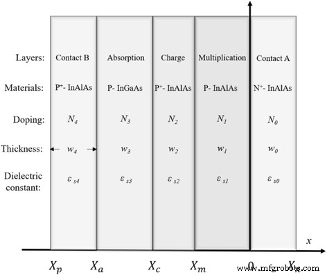
이 섹션에서는 장치 매개변수와 장치의 전계 분포 사이의 수학적 관계를 구축했으며 이를 적용하여 전하층과 터널링 효과를 분석했습니다. 동시에 시뮬레이션 구조, 재료 매개변수 및 기본 물리적 모델을 포함하는 시뮬레이션 모델이 구축되었습니다. 이론적 분석 모델 및 시뮬레이션 모델은 SAGCM InGaAs/InAlAs APD의 수직 구조를 기반으로 했습니다.
도핑 레벨, 두께, 재료 및 구조와 같은 장치 매개변수는 APD에서 전기장 분포를 계산하기 위한 수학적 모델을 구축하는 데 사용되었습니다. Poisson 방정식, 공핍층 모델, 반도체 소자의 PN 접합 모델을 포함하는 기본 물리 이론은 [23], [24]의 1, 2, 4장에서 찾을 수 있습니다. 접합 곱셈 계수 방정식은 [25]에서 찾을 수 있으며 반도체의 재료 매개변수는 [26]에서 찾을 수 있습니다. 제시된 모델은 Poisson 방정식, 터널링 전류 밀도 방정식, 공핍층 모델, 접합 이론 모델 및 애벌랜치 이득의 로컬 모델을 채택합니다. 기본 구조 매개변수(재료, 두께, 도핑 및 유전 상수)를 포함하는 APD의 단순화된 수학적 좌표 시스템은 그림 1에 나와 있습니다. 이것은 그레이딩 레이어를 무시하는 단순화된 SACM APD 구조입니다. 접촉층, 전하층, 증배층의 재료는 InAlAs, 흡수층은 InGaAs이다. 레이어의 접합은 X로 구분됩니다. n , 0, X m , X ㄷ , 및 X 아 및 X p x 동등 어구. 도핑 수준은 N으로 표시됩니다. 0 , N 1 , N 2 , N 3 , 및 N 4 , 레이어 두께는 w로 표시됩니다. 0 , w 1 , w 2 , w 3 , 및 w 4 , 유전 상수는 ε로 표시됩니다. 0 , ε s1 , ε s2 , ε s3 , 및 ε s4 접점 A, 곱셈, 전하, 흡수 및 접점 B의 각각.
<그림>
SACM InGaAs/InAlAs APD의 단순화된 수학적 좌표계. 이론적 모델을 구축하는 데 사용되는 APD의 단순화된 구조를 제시합니다. 기본 구조 매개변수(재료, 두께, 도핑 및 유전 상수)를 포함하는 APD의 단순화된 수학적 좌표계
장치 매개변수로 푸아송 방정식을 풀면 최대 전기장의 수학적 표현이 얻어집니다. 이 식은 식 2, 3과 같이 공핍층의 침투 두께 변화에 의해 결정된다. 이 식에서 도핑 레벨(N ), 공핍층의 두께(w ) 및 유전 상수(ε) 그림 1에서 다양한 레이어를 찾을 수 있습니다.
$$ {\xi}_{\max (w)}={\sum}_{k=1}^4\left(-\frac{q\times {N}_k\times {w}_k}{\ varepsilon_{sk}}\right) $$ (2) $$ {\xi}_{\max (w)}=\frac{q\times {N}_0\times {w}_0}{\varepsilon_{s0 }} $$ (3)
그러면 수학식 4와 5를 이용하여 모든 점에서 전기장 분포를 도출할 수 있다. 경계 조건은 내장 전위 V를 무시한다. br 공식 6에서; 따라서 공핍층 두께와 바이어스 전압 사이의 수학적 관계를 계산할 수 있습니다.
$$ {\xi}_{\left(x,w\right)}={\xi}_{\max (w)}+{\sum}_{k=1}^4\left(\frac{ q\times {N}_k\times \left|x\right|}{\varepsilon_{sk}}\right)\left({X}_p
마지막으로, 장치의 전기장 분포와 바이어스 전압 사이의 수학적 관계는 공식 7–11을 사용하여 얻습니다. $$ \xi \left(x,{V}_{\mathrm{편향}}\right)={\xi}_{\max \left({V}_{\mathrm{편향}}\right)} +\frac{q\times {N}_1\times \left|x\right|}{\varepsilon_{s1}}\left(0\ge x\ge {X}_m\right) $$ (7) $ $ \xi \left(x,{V}_{\mathrm{편향}}\right)={\xi}_{\max \left({V}_{\mathrm{편향}}\right)}+ \frac{q\times {N}_1\times {w}_1}{\varepsilon_{s1}}+\frac{q\times {N}_2\times \left|x-{X}_m\right|} {\varepsilon_{s2}}\left({X}_m\ge x\ge {X}_c\right) $$ (8) $$ \xi \left(x,{V}_{\mathrm{bias} }\right)={\xi}_{\max \left({V}_{\mathrm{bias}}\right)}+\frac{q\times {N}_1\times {w}_1}{ \varepsilon_{s1}}+\frac{q\times {N}_2\times {w}_2}{\varepsilon_{s2}}+\frac{q\times {N}_3\times \left|x-{ X}_c\right|}{\varepsilon_{s3}}\left({X}_c\ge x\ge {X}_a\right) $$ (9) $$ \xi \left(x,{V} _{\mathrm{편향}}\right)={\xi}_{\max \left({V}_{\mathrm{편향}}\right)}+\frac{q\times {N}_1\ 시간 {w}_1}{\varepsilon_{s1}}+\frac{q\times {N}_2\times {w}_2}{\varepsilon_{s2}}+\frac{q\times {N}_3\ 배 {w}_3}{\varepsilon_{s3}}+\frac{q\times {N}_4\times \left|x-{X} _a\right|}{\varepsilon_{s4}}\left({X}_a\ge x\ge {X}_p\right) $$ (10) $$ \xi \left(x,{V}_{ \mathrm{편향}}\right)={\xi}_{\max \left({V}_{\mathrm{편향}}\right)}-\frac{q\times {N}_0\times x }{\varepsilon_{s0}}\left(0\le x\le {X}_n\right) $$ (11)
모델에서 공핍층의 경계가 접촉 영역에 도달하면 공식 7-11을 사용하여 각 층의 전기장을 분석할 수 있습니다. 실제 APD에서 흡수 및 증배층은 의도하지 않게 진성층에 도핑됩니다. 아니 3 및 N 1 N 미만 2 . 따라서 공식 9는 공식 12와 거의 같습니다. 전하층이 소자의 전계 분포를 제어할 수 있는 이유입니다.
$$ {\displaystyle \begin{array}{l}\xi \left(x,{V}_{\mathrm{bias}}\right)={\xi}_{\max \left({V}_ {\mathrm{편향}}\right)}+\frac{q\times {N}_1\times {w}_1}{\varepsilon_{s1}}+\frac{q\times {N}_2\times { w}_2}{\varepsilon_{s2}}+\frac{q\times {N}_3\times \left|x-{X}_c\right|}{\varepsilon_{s3}}\\ {}\kern4em \approx {\xi}_{\max \left({V}_{\mathrm{bias}}\right)}+\frac{q\times {N}_2\times {w}_2}{\varepsilon_{ s2}}\left({X}_{\mathrm{c}}\ge x\ge {X}_a\right)\end{배열}} $$ (12)
공식 8에서 곱셈과 흡수 사이의 전기장 차이는 N의 곱을 사용하여 결정됩니다. 2 그리고 w 2 . 아니 2 는 전하 층의 도핑 수준이고 w 2 는 전하층 두께입니다. InGaAs/InAlAs APD에서 적절한 전계 분포를 위해 흡수층(InGaAs)의 전계는 광유도 캐리어에 충분한 속도를 보장하고 터널링 효과를 피할 수 있는 50–180kV/cm의 간격 값 내에 있어야 합니다. 흡수층[10]에서. 즉, 곱셈의 애벌랜치 필드는 전하층에 의한 흡수에서 50–180kV/cm로 감소해야 합니다. 따라서 공식 8을 사용하여 최적의 계산된 도핑 레벨과 전하층의 두께를 찾을 수 있습니다. 곱셈 레이어가 200nm일 때(애벌랜치 필드 E 곱셈에서 6.7 × 10
5
V/cm 동안 곱셈 레이어는 200nm[27]); 계산된 전하층의 도핑 수준 및 두께 값은 [28,29,30,31,32,33]의 결과와 그림 2의 결과와 비교됩니다. 이론 값의 영역은 실험 데이터와 잘 일치합니다. 이 결과는 곱셈 두께가 확실할 때 공식 8을 사용하여 전하층에서 두께가 다른 도핑 수준을 예측하는 데 사용할 수 있음을 증명합니다.
<사진> 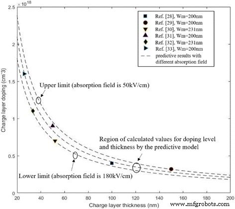
다양한 보고서의 이론적 결과와 실험 데이터 비교(w m =200nm). 닫힌 기호:참조에서 200nm(검은색 정사각형, 검은색 원, 검은색 삼각형, 검은색 오른쪽 삼각형) 및 231nm(검은색 다이아몬드, 검은색 아래쪽 삼각형)의 곱셈 두께를 갖는 전하 층의 도핑 수준 및 두께. 계산된 전하층(도핑 레벨 및 두께) 값을 공식 8로 표시합니다(흡수 필드는 50–180kV/cm임). 흡수 필드가 50kV/cm일 때 전하층의 도핑 레벨의 상한을 얻을 수 있습니다. 흡수 필드가 180kV/cm일 때 전하층의 도핑 수준의 하한을 얻을 수 있습니다. 다양한 보고서의 이론적 결과와 실험 데이터를 비교합니다. 이론 값의 영역은 실험 데이터와 잘 일치합니다. 점선은 공식에 의한 도핑 수준 및 두께의 계산된 값
300, 500, 700nm의 곱셈층을 사용하여 전하층의 다양한 두께에 대한 최적의 도핑 수준을 계산하고 그 결과를 그림 3에 나타내었습니다. 이 결과는 전하층의 도핑 수준의 허용 오차가 다음과 같다는 것을 보여줍니다. 전하층의 두께가 증가함에 따라 두께 및 도핑 레벨의 범위와 관련하여 감소합니다. 즉, 두꺼운 전하 영역을 적용할 경우 최적의 전기장을 만족시키기 위해 전하층의 작은 범위의 도핑 레벨만 존재하게 됩니다. 결과적으로 APD의 성능은 두꺼운 전하층에서 도핑 농도의 몇 퍼센트 편차를 통해 크게 달라집니다. "결과 및 논의" 섹션에서는 APD의 실제 구조를 시뮬레이션하여 이론적인 분석을 연구하고 검증했습니다. 여기에는 전하층의 도핑 레벨 범위에 대한 전하층 두께의 영향과 다양한 전하층 두께에 대한 성능의 다양성이 포함됩니다. APD.
<그림> 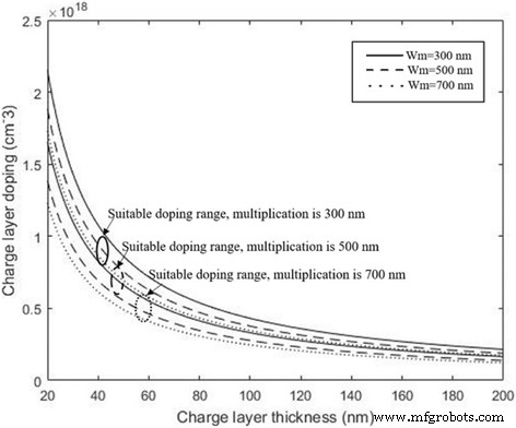
다양한 증배층에 대한 최적의 도핑 레벨 및 전하층 두께. 실선:w m =300nm. 파선:w m =500nm. 점선:w m =700nm 전하층의 계산된 값(도핑 레벨 및 두께)을 공식으로 제시하며 흡수층의 필드가 적합합니다. 곱셈 레이어의 두께는 300, 500, 700nm입니다. 곱셈층의 두께가 확실하면 공식을 사용하여 최적의 도핑 수준과 전하층의 두께를 찾을 수 있습니다.
터널링을 고려한 이론적 모델
위의 해석 모델은 소자의 전계 분포에 관한 것으로 ρ 공핍층의 도펀트 이온입니다. 충분히 높은 전기장이 흡수층 내에 존재한다면 국부 밴드 굽힘은 전자가 터널링되도록 하기에 충분할 수 있습니다[34]. 따라서 전자 터널링이 발생할 수 있습니다. 그림 4의 터널링 개략도에서 흡수층이 항복 터널링을 가질 때 터널링 효과는 전하 밀도 ρ를 변화시킵니다. , 흡수의 양전하가 증가하고 곱셈 및 전하층의 음전하가 증가합니다. 따라서 ρ 터널링 효과가 나타나는 동안 공핍층의 도펀트 이온 전하 밀도와 같지 않습니다. 앞서 논의한 공식은 터널링 효과를 고려하여 변경됩니다.
<그림> 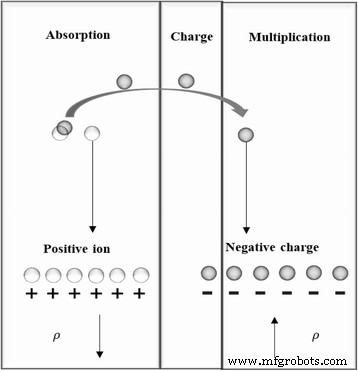
증배층과 흡수층의 터널링 과정과 전하 밀도 변화. 장치에서 터널링 프로세스의 개략도를 제공합니다. 충분히 높은 전기장이 흡수층 내에 존재하면 국부 밴드 굽힘이 전자가 터널링되도록 하기에 충분할 수 있습니다. 흡수층에 항복 터널링이 있는 경우 흡수층의 양전하가 증가하고 증배층 및 전하층의 음전하가 증가합니다. 따라서 ρ 터널링 효과가 나타나는 동안 공핍층의 도펀트 이온 전하 밀도와 같지 않음
발전율 G bbt 대역 대 대역 터널의 비율은 공식 13[35, 36]에 설명되어 있습니다.
$$ {G}_{bbt}={\left(\frac{2{m}^{\ast }}{E_g}\right)}^{1/2}\frac{q^2{E_p}^ {\감마 }}{{\left(2\pi \right)}^3{\hbar}^2}\exp \left(\frac{-\pi }{4{q\mathit{\hbar E}} _p}{\left(2{m}^{\ast}\times {E_g}^3\right)}^{\raisebox{1ex}{$1$}\!\left/ \!\raisebox{-1ex} {$2$}\right.}\right)=A\times {E_p}^{\gamma}\times \exp \left(-\frac{B}{E_p}\right) $$ (13)
공식 13에서 E g InGaAs의 에너지 밴드 갭, m* (0.04 m와 동일) e )는 유효 감소된 질량, E p 는 흡수층의 파괴 전계, γ 일반적으로 1~2로 제한되는 사용자 정의 매개변수입니다. A 그리고 B 특성화 매개변수입니다. G를 계산합니다. bbt 다른 γ , 그 결과를 Fig. 5에 나타내었다. G bbt γ 동안 전하층 도핑 레벨에 대해 동일한 크기 차수를 적용합니다. 1~1.5로 제한됩니다.
<그림> 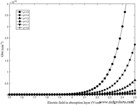
지 btt 다른 γ를 갖는 흡수층의 다른 필드에 대해 . γ의 값 1.0(검은색 별), 1.1(검은 아래쪽을 가리키는 삼각형), 1.2(검은 다이아몬드), 1.3(검은 삼각형), 1.4(검은 정사각형), 1.5(검은 원)입니다. G의 계산된 결과를 나타냅니다. btt 식 13에 의해 흡수영역이 19kV/cm를 초과하는 경우, G bbt 점차 증가합니다. 또한 G bbt γ 동안 전하층 도핑 레벨에 대해 동일한 크기 차수를 적용합니다. 1~1.5로 제한됨
결과적으로 전하 밀도 ρ 는 가변적이며 터널링 효과와 흡수 터널의 도펀트 이온에 의해 결정됩니다. 이때, 수학식 1을 수학식 14로 바꾸고, 곱셈층의 전기장을 수학식 15로 설명한다. w 터널 터널링 프로세스의 유효 공핍층이다[35]. 따라서 Avalanche Field의 변화는 식 16으로 설명할 수 있으며, Avalanche Field는 터널링 효과와 곱하여 감소하게 된다.
$$ \frac{d\xi}{dx}=\frac{\rho }{\varepsilon }=\frac{q\times \left(N+{G}_{btt}\right)}{\varepsilon }, {E}_p>
1.8\times {10}^5V/cm $$ (14) $$ \xi \left(x,{V}_{\mathrm{편향}}\right)={\xi}_{ \max \left({V}_{\mathrm{bias}}\right)}+\frac{q\times \left({N}_1\times \left|x\right|+{G}_{bbt }\times {w}_{\mathrm{tunnel}}\right)}{\varepsilon_{s1}}\left(0\ge x\ge {X}_m\right) $$ (15) $$ \delta \xi \left(x,{V}_{\mathrm{편향}}\right)=\delta E=\frac{q\times {G}_{btt}\times {w}_{\mathrm{tunnel }}}{\varepsilon_{\mathrm{s}3}} $$ (16)
전자 및 정공 이온화 계수는 [18]의 수학식 17 및 18로 설명됩니다. 이 곱셈의 눈사태 필드입니다.
$$ \alpha ={a}_n{e}^{\raisebox{1ex}{$-{b}_n$}\!\left/ \!\raisebox{-1ex}{$E$}\right.} $$ (17) $$ \베타 ={a}_p{e}^{\raisebox{1ex}{$-{b}_p$}\!\left/ \!\raisebox{-1ex}{$E$ }\right.} $$ (18)
캐리어 사태의 영향은 충격 이온화 모델에 의해 설명됩니다. 전하층에 비해 증배층의 매우 낮은 캐리어 밀도를 고려할 때, 전계는 증배층 전체에 걸쳐 균일하다고 가정하는 것이 합리적이다. 따라서 곱셈 계수(M n )는 다음 식과 같이 표현될 수 있다. 19. 여기, w m 는 곱셈 레이어 두께이고 k 는 α/β로 정의된 충격 이온화 계수 비율입니다. . k 이후로 전기장에 따라 매우 느리게 변합니다. k w의 약간의 변화에 대해 거의 일정합니다. m [37].
$$ {M}_n=\frac{k-1}{k\times {e}^{-\alpha \left(1-\raisebox{1ex}{$1$}\!\left/ \!\raisebox{ -1ex}{$k$}\right.\right){w}_m}-1} $$ (19)
상수 w를 가정 m 및 바이어스 전압, M의 미분 n 전자 이온화 계수와 관련하여 공식 20 및 21에 있습니다.
$$ \delta {M}_n\left|{}_{w=const\&V=const}\right.={M_n}^2{e}^{-\alpha \left(1-\raisebox{1ex} {$1$}\!\left/ \!\raisebox{-1ex}{$k$}\right.\right){w}_m}\times {w}_m\delta \alpha $$ (20) $$ \delta \alpha =\frac{\delta \alpha}{\delta E}={\alpha}_n{b}_n{e}^{\frac{-{b}_n}{E}}\frac{1 }{E^2} $$ (21)
식 20 및 21에서 δα/δE 긍정적이다. 전체 공핍 흡수층의 20%가 w라고 가정합니다. 터널 흡수층은 두께가 400nm입니다. 식 16을 풀면 δE 다른 γ의 흡수장 그림 6에 나와 있습니다. δE 곱셈에서 눈사태 필드에 대해 동일한 크기 차수를 적용합니다. 따라서 터널링 효과는 애벌랜치 필드에 영향을 미치고 M n 터널링 효과로 감소합니다. 분석에서는 곱셈에서 음전하가 곱해지지 않고 이를 고려하여 모델이 더 엄격해질 것이라고 가정했습니다. 터널링 효과가 APD의 실제 구조에 미치는 영향을 확인하고 분석하기 위해 "결과 및 논의" 섹션에서 터널링 효과와 증배 애벌랜치 필드 간의 관계를 시뮬레이션했습니다.
<사진> 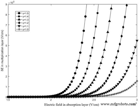
δE 다른 γ를 갖는 흡수층의 다른 필드에 대해 . γ의 값 1.0(검은색 별), 1.1(검은 아래쪽을 가리키는 삼각형), 1.2(검은 다이아몬드), 1.3(검은 삼각형), 1.4(검은 정사각형), 1.5(검은 원)입니다. δE의 계산된 결과를 나타냅니다. 식 16에 의해. 흡수장이 19kV/cm를 초과할 때, δE 점차 증가합니다. 또한 δE 곱셈에서 눈사태 필드에 대해 동일한 크기 차수를 적용합니다. 따라서 터널링 효과는 터널링 효과와 함께 애벌랜치 필드에 영향을 미칩니다.
구조 및 시뮬레이션 모델
시뮬레이션 및 분석에는 TCAD의 반도체 소자 시뮬레이션을 사용하였다. 이 시뮬레이션 엔진은 시뮬레이션에서 물리적 모델을 정의하고 그 결과는 물리적 의미를 갖는다[20]. 기본적인 물리적 모델은 다음과 같이 제시되었다. Poisson 및 캐리어 연속성 방정식을 포함한 드리프트-확산 모델을 사용하여 전기장 분포 및 확산 전류 IDIFF를 시뮬레이션했습니다. . 대역 대 대역 터널링 모델은 대역 대 대역 터널링 전류 IB2B에 사용되었습니다. , 그리고 트랩 보조 터널링 모델은 트랩 보조 터널링 전류 ITAT에 사용되었습니다. . 세대-재결합 전류 IGR Shockley-Read-Hall 재결합 모델 및 Auger 재결합 전류 IAUGER에 의해 설명되었습니다. Auger 재조합 모델에 의해 설명되었습니다. 암전류는 이러한 메커니즘에 의해 명확하게 설명되었습니다[38]. 눈사태 곱셈은 Selberherr 충격 이온화 모델에 의해 설명되었습니다. Fermi-Dirac 캐리어 통계, 캐리어 농도 종속, 낮은 필드 이동성, 속도 포화 및 광선 추적 방법을 포함한 기타 기본 모델이 시뮬레이션 모델에 사용되었으며 엄격한 시뮬레이션 모델이 구축되었습니다.
시뮬레이션의 장치 구조는 [13]의 실험 구조와 유사했습니다. 상부 조명 SAGCM InGaAs/InAlAs APD의 개략적인 단면은 그림 7에 나와 있습니다. 구조는 위에서 아래로 InGaAs 접촉층, InAlAs 클래딩층, InAlGaAs 등급층, InGaAs 흡수층, InAlGaAs 등급으로 순차적으로 명명됩니다. 층, InAlAs 전하 층, InAlAs 증배 층, InAlAs 클래딩 층, InP 접촉 층 및 InP 기판. 각 레이어의 두께와 도핑도 그림 7에 나와 있습니다. 시뮬레이션 결과에 대한 두께의 영향을 피하기 위해 두 가지 시뮬레이션 구조를 선택했습니다. 하나의 시뮬레이션 구조는 APD-1(곱셈 및 흡수 레이어는 각각 800 및 1800nm)으로 명명되고 다른 시뮬레이션 구조는 APD-2(곱셈 및 흡수 레이어는 각각 200 및 600nm)로 명명됩니다. <그림> 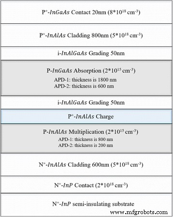
APD의 시뮬레이션 구조 및 매개변수. 상부 조명 SAGCM InGaAs/InAlAs APD-1 및 APD-2의 개략적인 단면을 제시합니다. 여기에는 구조, 재료, 도핑 및 두께가 포함됩니다.
시뮬레이션 모델을 검증하기 위해 [13]의 실험 데이터를 시뮬레이션 결과와 비교하였다. 이 시뮬레이션에서는 레퍼런스와 동일한 구조를 사용했고, 소자의 전류-전압 특성이 주어졌다. 그림 8은 시뮬레이션 결과와 참조의 실험 결과를 보여줍니다. 그들은 유사한 펀치 스루 전압 V을 가지고 있습니다. pt 및 항복 전압 V br . 또한 시뮬레이션과 실험 결과가 잘 일치합니다. 따라서 시뮬레이션의 모델은 정확합니다. 위에서 언급한 매개변수는 표 1에 나열되어 있습니다.
<사진> 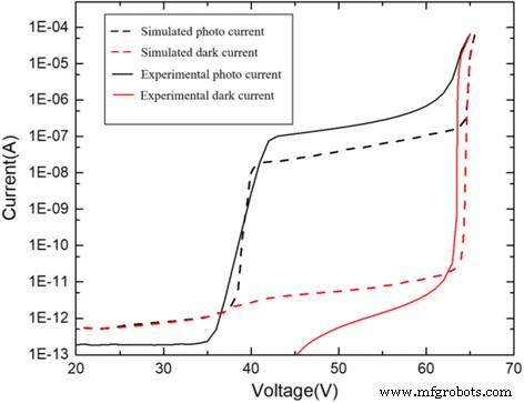
실험 결과와 비교한 시뮬레이션 결과(광전류 및 암전류). 검은색 점선:시뮬레이션된 광전류. 빨간색 점선:시뮬레이션된 암전류. 검은색 실선:실험적 광전류. 빨간색 실선:실험적 암전류. 시뮬레이션 결과와 실험 결과의 비교를 제시합니다. 시뮬레이션 모델은 참조 실험의 동일한 매개변수를 사용합니다.
결과 및 토론
본 절에서는 시뮬레이션을 통해 이론적 분석과 결론을 구체적으로 연구하였다. 먼저, "전하층 두께의 영향" 섹션에서 전하층의 도핑 레벨 허용오차에 대한 전하층 두께의 영향을 연구했습니다. 그런 다음 "전기장 분포에 대한 터널링 효과" 섹션에서 터널링 효과와 증배 눈사태 필드 간의 관계를 분석하고 확인했습니다.
전하층 두께의 영향
[14]에서 InGaAs/InAlAs APD의 적절한 필드 분포는 이러한 규칙을 준수해야 합니다. 보증 V pt <V br 및 V br − V pt 온도 변동 및 작동 범위의 변화를 처리하기 위한 안전 여유가 있어야 합니다. 흡수층에서 전기장은 광유도 캐리어에 충분한 속도를 보장하기 위해 50~100kV/cm보다 커야 합니다. 동시에 전기장은 흡수층에서 터널링 효과를 피하기 위해 180kV/cm 미만이어야 합니다. 전기장 분포는 장치 성능에 큰 영향을 미칩니다. 흡수층에서 전기장의 선택은 실제 요구 사항에 대한 작은 통과 시간, 암전류 및 높은 응답성 간의 균형을 유지합니다.
In the simulation, we used the structure of APD-1 (multiplication is 800 nm thick) and adjusted the charge layer thickness from 50 to 210 nm to study the influence of charge layer thickness on doping level range and verify the theoretical conclusions in analytical model. In the simulation, we selected different doping level ranges in the charge layer so that the electric field distribution complies with the rules. The simulation results on the relationship between thickness and doping level range in the charge layer are presented in Fig. 9a. As the charge layer thickness increases, the suitable doping level range in charge layer decreases. A relatively large doping level range exists in the thin charge layer, and under this doping level range, the device will have a suitable electric field distribution. Apparently, the doping level range is determined by charge layer thickness. The simulation result of APD-2 (with a thickness of multiplication of 200 nm) is presented in Fig. 9b, which has a similar result. Moreover, it can be found that the calculated results of Fig. 2 and simulation results of Fig. 9b match well as shown in Fig. 9c. The small difference between the calculated results and simulation results is caused by the different values of avalanche field in the simulation and calculation. The avalanche field in simulation engine is used 6.4 × 10
5
V/cm, while in the calculation, we use the value of 6.7 × 10
5
V/cm from [27].
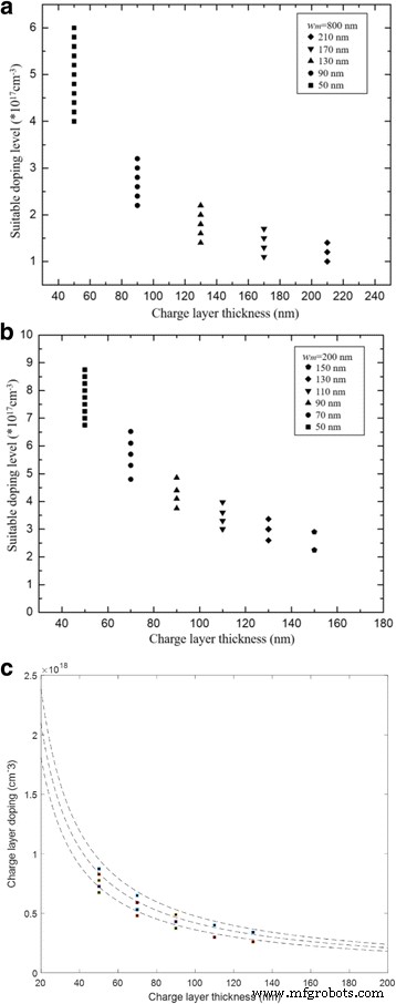
아 Relationship between suitable doping level and thickness of charge layer (APD-1). The thickness of charge layer is 50 nm (black square), 90 nm (black circle), 130 nm (black triangle), 170 nm (black down-pointing triangle), 210 nm (black diamond). 아 presents the suitable doping level region for different thickness of charge layer. As the charge layer thickness increases, the suitable doping level range in the charge layer decreases. A relatively large doping level range exists in the thin charge layer, and under this doping level range, the device will have a suitable electric field distribution. Apparently, the doping level range is determined by charge layer thickness. ㄴ Relationship between suitable doping level and thickness of charge layer (APD-2). The thickness of charge layer is 50 nm (black square), 70 nm (black circle), 90 nm (black triangle), 110 nm (black down-pointing triangle), 130 nm (black diamond), and 150 nm (black pentagon). The figure description of b is similar to a . ㄷ Comparison of calculated results in Fig. 2 and simulated results in Fig. 9b. Dashed line:calculated results. Closed symbols:simulated results (black square). ㄷ presents the comparison of calculated results in Fig. 2 and simulated results in Fig. 9b. The calculated results and simulated results correspond well
The charge layer thicknesses of 210 and 50 nm (APD-1) were selected to show the simulation details and the influence of doping level on the electric field distribution. Figure 10a, c shows the current simulation results of different doping levels in thicknesses of 210 and 50 nm, respectively. Figure 10b, d shows the electric field distribution simulation results using the same structure. The simulation results show that thicknesses of 210 and 50 nm have doping level ranges of 1.0 × 10
17
–1.3 × 10
17
cm
−3
and 3.9 × 10
17
–5.7 × 10
17
cm
−3
, 각각.
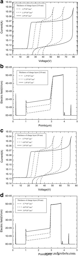
아 Photocurrent and dark current with different doping level (thickness of charge layer is 210 nm). Solid line:doping level in the charge layer is 1.3 × 10
17
cm
−3
. Dashed line:doping level in charge layer is 1.15 × 10
17
cm
−3
. Dashed dot line:doping level in charge layer is 1.0 × 10
17
cm
−3
. 아 Presents the simulation results of currents with different doping level. The device with a charge layer thickness of 210 nm only has a relatively narrow and suitable doping level. A minimal change in the doping level has greatly influence the punch-through voltage, breakdown voltage, and current-voltage characteristic. ㄴ Avalanche field with different doping level (thickness of charge layer is 210 nm). Solid line:doping level in charge layer is 1.3 × 10
17
cm
−3
. Dashed line:doping level in charge layer is 1.15 × 10
17
cm
−3
. Dashed dot line:doping level in charge layer is 1.0 × 10
17
cm
−3
. ㄴ Presents the simulation results of fields with different doping level. The device with a charge layer thickness of 210 nm only has a relatively narrow and suitable doping level. A minimal change in the doping level has greatly influenced the electric field distribution. ㄷ Photocurrent and dark current with different doping level (thickness of charge layer is 50 nm). Solid line:doping level in charge layer is 5.7 × 10
17
cm
−3
. Dashed line:doping level in charge layer is 4.8 × 10
17
cm
−3
. Dashed dot line:doping level in charge layer is 3.9 × 10
17
cm
−3
. ㄷ Presents the simulation results of currents with different doping level. The device with a charge layer thickness of 50 nm has a relatively wide and suitable doping level. A minimal change in the doping level has a small influence on the current-voltage characteristic. d Avalanche field with different doping level (thickness of charge layer is 50 nm). Solid line:doping level in charge layer is 5.7 × 10
17
cm
−3
. Dashed line:doping level in charge layer is 4.8 × 10
17
cm
−3
. Dashed dot line:doping level in charge layer is 3.9 × 10
17
cm
−3
. d Presents the simulation results of fields with different doping level. The device with a charge layer thickness of 50 nm only has a relatively wide and suitable doping level. A minimal change in the doping level has a small influence on the electric field distribution
Clearly, the device with a charge layer thickness of 210 nm only has a relatively narrow and suitable doping level. A minimal change in the doping level has greatly influence the current-voltage characteristic and electric field distribution. As a result, the performance of APD varies significantly via several percent deviations of doping concentrations in the thicker charge layer. This conclusion is the same as the theoretical analysis. Concurrently, when designing APD structures, choosing a thin charge layer will give a high level of doping tolerance, as well as confer APD with good controllability.
Finally, the relationship between charge layer and multiplication thickness was simulated. Figure 11a presents the avalanche field with multiplication region thicknesses of 100, 200, and 300 nm in the APD-2 structure (with a charge layer thickness of 70 nm). Figure 11b presents the charge layer doping range with different multiplication thicknesses at the suitable electric field distribution condition. The charge layer thicknesses are 50, 70, and 90 nm. Clearly, a high avalanche field exists in the thin multiplication layer. As the multiplication region thickness decreases, the electric field difference between multiplication and absorption layers increases. As a result, a thin multiplication layer needs a high product of the charge layer doping level and thickness to reduce the high avalanche field.
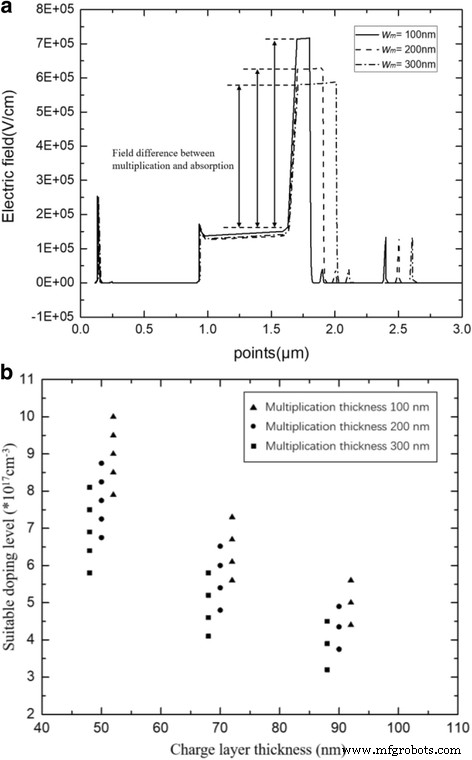
아 Avalanche breakdown electric field with different multiplication thicknesses. Solid line:w m = 100 nm. Dashed line:w m = 200 nm. Dashed dot line:w m = 300 nm. 아 Presents the simulation results of electric field distribution with different w m . As the w m decreases, the avalanche field in the multiplication increase. ㄴ Relationship between multiplication thickness and charge layer. The thickness of multiplication is 300 nm (black square), 200 nm (black circle), 100 nm (black triangle). ㄴ Presents the relationship between multiplication thickness and charge layer. A thin multiplication layer needs a high product of the charge layer doping level and thickness to reduce the high avalanche field
Tunneling Effect on the Electric Field Distribution
The simulation in this part will study the tunneling effect on the electric field in the device. From the theoretical analysis, the tunneling effect has an influence on the avalanche field in multiplication. Thus, the simulation will design to study the influence of electric field in the absorption layer that exceeds the tunneling threshold value. First, group A, with the structure of APD-1, charge layer thickness of 90 nm, and different charge layer doping levels of 1.4 × 10
17
–2.4 × 10
17
cm
−3
, was simulated for electric field distribution when the device avalanche breaks down. The result is shown in Fig. 12a. When the charge layer doping level exceeds 2.0 × 10
17
cm
−3
, the field in the absorption layer becomes lower than the tunneling threshold field and the avalanche field in the multiplication layer reaches the same value. However, when the doping level is less than 2.0 × 10
17
cm
−3
, the field in the absorption layer exceeds the tunneling threshold field and the avalanche field in the multiplication layer decreases with the decrease of the doping level in charge layer. Similar results were observed in the APD-2 structure (with a charge layer thickness of 90 nm and doping level of 2.2 × 10
17
–3.6*10
17
cm
−3
) (Fig. 12b). That is, if the electric field in the absorption layer exceeds the tunneling threshold value at or over the breakdown voltage, then the breakdown electric field in the multiplication will decrease.
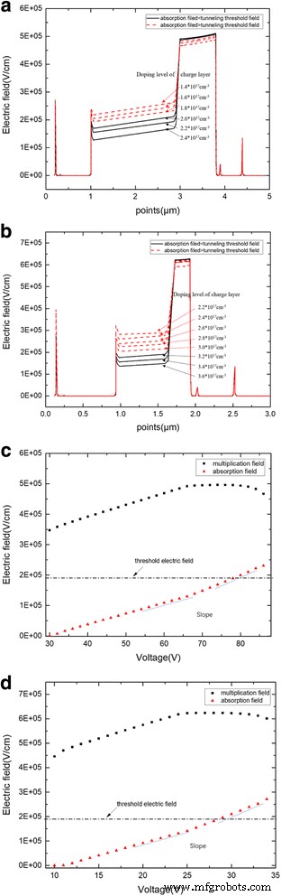
아 Avalanche breakdown electric field with different doping levels (APD-1). Thickness of charge layer is 90 nm. Red dashed lines:the field of absorption is larger than the tunneling threshold field. Black solid lines:the field of absorption is less than the tunneling threshold field. 아 Presents the simulation results of electric field distribution with different doping level while avalanche breakdown. When doping level of charge layer exceeds 2.0 × 10
17
cm
−3
, the field in the absorption layer becomes lower than the tunneling threshold field, and the avalanche field in the multiplication layer reaches the same value with different doping level. However, when the doping level is less than 2.0 × 10
17
cm
−3
, the field in the absorption layer exceeds the tunneling threshold field, and the avalanche field in the multiplication layer decreases with the decrease of the doping level. Thus, if the electric field in the absorption layer exceeds the tunneling threshold value at or over the breakdown voltage, then the breakdown electric field in the multiplication will decrease. Thus, the electric field in the absorption should be less than the tunneling threshold value to maintain the high field in the multiplication layer when the device avalanche breaks down. ㄴ Avalanche breakdown electric field with different doping levels (APD-2). Thickness of charge layer is 90 nm. Red dashed lines:the field of absorption is larger than the tunneling threshold field. Black solid lines:the field of absorption is less than the tunneling threshold field. The figure description of b is similar to a . ㄷ Relationship between field and bias voltage in multiplication and absorption (APD-1). Thickness of charge layer is 90 nm. Electric field of multiplication (black square). Electric field of absorption (red triangle). ㄷ Presents the relationship between the electric field and bias voltage in multiplication and absorption layers. When the electric field in the absorption layer reaches the tunneling threshold value, the avalanche breakdown electric field in the multiplication gradually decreases. Moreover, the absorption field slope increases when the electric field in the absorption layer exceeds the tunneling threshold. d Relationship between field and bias voltage in multiplication and absorption (APD-2). Thickness of charge layer is 90 nm. Electric field of multiplication (black square). Electric field of absorption (red triangle). The figure legend of d is similar to a
Groups B (APD-1 thickness of 90 nm, doping level of 2.4 × 10
17
cm
−3
in charge layer and APD-2 thickness of 90 nm, doping level of 3.6 × 10
17
cm
−3
) were designed to demonstrate the relationship between the threshold electric field in the absorption layer and avalanche field in the multiplication layer. The multiplication and absorption electric fields vary with the bias voltage on the device. As shown in Fig. 12c, d, when the electric field in the absorption layer reaches the tunneling threshold value, the avalanche breakdown electric field in the multiplication gradually decreases. Moreover, when the absorption field exceeds the tunneling threshold, the avalanche breakdown electric field in the multiplication layer plummets. Furthermore, the absorption field slope increases when the electric field in the absorption layer exceeds the tunneling threshold.
The phenomenon in Fig. 12 can be explained by the theoretical analysis that tunneling has an influence on the charge density in the “Methods” section. When the electric field reaches the tunneling threshold value in the absorption layer, the charge density ρ becomes unequal to the dopant ion. The multiplication field will decrease as the negative ion increases, and the absorption field will increase as the positive ion increases. Concurrently, the absorption field slope will increase due to the tunneling effect. As a result, the electric field in the absorption should be less than the tunneling threshold value to maintain the high field in the multiplication layer and the low dark current when the device avalanche breaks down.
결론
In summary, we have presented a theoretical study and numerical simulation analysis involving the InGaAs/InAlAs APD. The mathematical relationship between the device parameters and electric field distribution in the device was built. And the tunneling effect was taken into consideration in the theoretical analysis. Through analysis and simulation, the influence of structure parameters on the device and the detailed relationship of each layer were fully understood in the device. Three important conclusions can be obtained from this paper. First, the doping level and thickness of the charge layer for different multiplication thicknesses can be calculated by the theoretical model in the “Methods” section. Calculated charge layer values (doping and thickness) are in agreement with the experiment results. Second, as the charge layer thickness increases, the suitable doping level range in charge layer decreases. Compared to the thinner charge layer, the performance of APD varies significantly via several percent deviations of doping concentrations in the thicker charge layer. When designing APD structures, choosing a thin charge layer will give a high level of doping tolerance, as well as confer APD with good controllability. Finally, the G btt of tunneling effect was calculated, and the influence of tunneling effect on the avalanche field was analyzed. We confirm that the avalanche field and multiplication factor (M n ) in the multiplication will decrease by the tunneling effect.
약어
- 2D:
-
2차원
- APD:
-
Avalanche photodiode
- DCR:
-
Dark count rate
- SACM APDs:
-
Separate absorption, charge, and multiplication avalanche photodiodes
- SAGCMAPDs:
-
Separate absorption, grading, charge, and multiplication avalanche photodiodes
- SPAD:
-
Single-photon avalanche photodiode
- SPDE:
-
Single-photon detection efficiency
- SRH:
-
Shockley–Read–Hall