고유한 그래핀 공진기가 있는 시스템에서 두 개의 전환 가능한 플라즈몬으로 유도된 투명도 효과
초록
PIT(plasmonically induced transparent) 효과를 구현하기 위한 일반적인 플라즈몬 시스템은 주로 하나의 단일 결합 경로만 허용하기 때문에 하나의 단일 PIT만 존재합니다. 이 연구에서 우리는 두 개의 전환 가능한 PIT 효과를 달성하기 위해 유전체 격자가 장착된 그래핀 층 공진기와 결합된 그래핀 나노리본(GNR)으로 구성된 별개의 그래핀 공진기 기반 시스템을 제안합니다. 공진기의 교차 방향을 설계함으로써 제안된 시스템은 서로 다른 공진 위치와 선폭을 특징으로 하는 두 가지 서로 다른 PIT 효과가 존재합니다. 이 두 가지 PIT 효과는 두 개의 분리된 편광 선택적 결합 경로에서 발생하므로 단순히 편광 방향을 변경하여 PIT를 서로 전환할 수 있습니다. 커플링 효과를 입증하기 위해 매개변수 연구가 수행되는 반면, 물리적 메커니즘을 설명하기 위해 2-입자 모델이 적용되어 수치적 결과와 이론적 결과 사이에 탁월한 일치를 찾습니다. 우리의 제안은 조정 가능한 이중 대역 센서 및 완벽한 흡수 장치와 같은 전환 가능한 PIT 기반 플라즈몬 장치를 설계하는 데 사용할 수 있습니다.
소개
표면 플라즈몬은 절연 매체와 전도 매체 사이의 계면에서 생성되는 자유 전자의 집합적인 공진 모드입니다[1, 2]. 입사 전자기장을 하위 파장 범위에서 원자 1개 규모의 극한 크기로 제한하는 능력으로 인해 [3], 표면 플라즈몬은 강한 광물질 상호 작용을 달성하는 가장 기본적이고 중요한 방법 중 하나가 되었습니다 [4] . 이 매력적인 광학 현상은 다양한 유형의 플라즈몬 시스템에서 발견되어 바이오 센싱[5], 비선형 광학[6, 7], 흡수체[8,9]와 같은 다양한 첨단 응용 분야의 개발을 촉진합니다. ,10,11] 및 기타 플라즈몬 변조기 [12,13,14,15]. 이러한 중요한 응용을 달성할 수 있는 가능성은 플라즈몬 유도 투명도(PIT)와 같은 몇 가지 흥미로운 현상에 기인합니다. PIT로 알려진 프로세스는 근거리 결합 Fano 간섭의 결과이며 시스템에서 공명 흡수를 제거하므로 광학 스펙트럼에서 두드러진 창을 생성하는 것이 특징입니다. 지난 몇 년 동안 이러한 일관된 플라즈몬 상호작용은 플라즈몬 스위칭[16], 느린 광 전파[17] 및 감지[18], 광학 저장[19]과 같은 다양한 응용 분야를 달성하는 데 사용되었습니다.
최근 연구에서 원자 두께까지의 초박형 금속 필름이 동적 전기적 조정성을 가질 수 있음이 밝혀졌지만[20, 21], 이러한 새로운 금속에 의해 지지되는 플라즈몬은 여전히 금속의 상대적으로 큰 저항 및 복사 손실을 겪고 있습니다[22, 23]. 이러한 금속의 단점은 금속 지지 PIT의 추가 개발을 제한하고 새로운 플라즈몬 재료를 찾는 것이 필요합니다. 금속 플라즈몬과 대조적으로 그래핀(대칭 육각형 벌집 격자로 형성된 촘촘하게 구조화된 탄소 원자의 단일 원자 층)에 의해 지지되는 플라즈몬은 정전기 바이어스[24, 25]를 통해 연속적이고 동적으로 조정될 수 있을 뿐만 아니라 긴 전파를 갖습니다. 새로운 세대의 재구성 가능한 플라즈몬 장치를 가능하게 하여 능동 PIT를 달성하기 위한 이상적인 플랫폼을 제공합니다[26, 27]. 순수한 금속[16, 28,29,30,31] 및 그래핀[32,33,34,35,36,37,38,39,40,41,42]에서 PIT를 달성하기 위해 다양한 재료와 디자인이 사용되었지만 , 또는 그들의 하이브리드 재료 기반 [43,44,45] 시스템, 이러한 시스템의 대부분은 단일 PIT 효과만 실현할 수 있습니다. 예를 들어, PIT를 달성하는 일반적인 방법 중 하나는 π를 설계하는 것입니다. -모양/유사 메타표면 [16, 28, 30, 33, 37, 45]. 또 다른 방법은 격자 결합 시스템을 구성하는 것입니다[32, 34]. 그러나 이러한 종류의 구조는 편광 종속 단일 창 PIT만 구현할 수 있습니다. 이는 이러한 구조의 특수한 기하학적 비대칭으로 인해 모든 나노구조 공진기가 밝은(복사/초복사) 또는 어두운(비복사/하복사) 모드로 작동하도록 미리 설정되어 있기 때문입니다. 따라서 그들은 하나의 특정 편광 방향에서 하나의 밝은 커플링 경로에서 어두운 커플링 경로만 허용하므로 하나의 편광 종속 PIT 효과만 발생합니다. 우리의 이전 연구는 순수한 그래핀 나노리본(GNR)[35] 또는 격자 결합 구조[38]에서 두 개의 명암 모드 결합 경로를 가진 PIT 시스템을 보여주었지만, 탈리 편광에 둔감한 단일 창 PIT 또는 편광 의존 이중 이러한 시스템의 창 PIT 효과는 기하학적 매개변수의 특정 선택에 크게 의존합니다(토론 부분 참조).
이 논문에서 우리는 두 개의 개별적인 PIT 효과를 결합하고 실현하기 위해 유전체 격자가 로드된 그래핀 시트와 결합된 GNR, 즉 두 개의 별개의 공진기를 사용할 것을 제안합니다. 우리는 수직 공진 방향을 설정함으로써 두 공진기에서 공진하는 표면 플라즈몬이 입사광의 다른 편광 방향에서 생성되어 두 개의 다른 편광 종속 결합 경로와 두 개의 개별 PIT 효과가 발생함을 입증할 것입니다. 또한 매개변수 연구를 통해 결합 메커니즘을 자세히 조사할 예정입니다. 그리고 고급 시뮬레이션과 2-입자 모델 기반 이론 분석이 결합되어 이러한 전환 가능한 PIT 효과를 보여줍니다. 마지막으로 굴절률 센서 및 완전 흡수체와 같은 제안된 시스템의 잠재적인 응용과 다른 PIT 시스템과의 비교에 대해 논의합니다.
디자인 및 자료
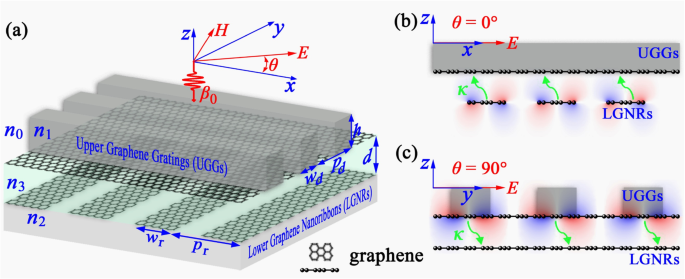
이 부분에서는 본 연구에 사용된 수치 모델과 관련 재료를 소개한다. 우리는 우리 모델에서 고전적 전기역학만을 고려하고 GNR의 가능한 양자 유한 크기 효과, 그래핀의 비선형 효과 및 기질 포논 효과에서 발생할 수 있는 효과를 무시한다고 명시합니다[46]. 제안된 시스템의 개략도는 그림 1에 나와 있습니다. 두 개의 그래핀 층이 x 오이 평면 및 도핑된 Si 또는 SiO2에 의해 분리됨 굴절률이 n인 전도체 3 및 두께 d . 첫 번째 층은 x 주기의 하부 그래핀 나노리본(LGNR)으로 형성됩니다. 방향. 두 번째 층은 전체 그래핀 시트로 굴절률이 n인 유전체 격자로 더 덮여 있습니다. 1 (상단 그래핀 격자, UGG로 표시됨) 및 마침표 Pdy에서 방향. 기하학적 매개변수는 W로 고정됩니다. r =와d =50 nm, pr =피d =100 nm, h =100 nm 및 d =20 nm, 그림 1에서 정의됨. 그래핀 층을 둘러싼 다른 물질의 유전 상수는 n으로 설정됨 0 그리고 n2 , 그림 1에 나와 있습니다. 단순화를 위해 일반성을 잃지 않고 유전 상수는 n으로 가정합니다. 1 =2.0 및 n0 =n2 =n3 =1.0. 굴절률의 허수부를 무시한다고 해서 이 연구의 근본적인 결론이 바뀌지는 않을 것입니다. 위의 매개변수는 달리 지정하지 않는 한 동일하게 유지됩니다. 기술적으로 설계된 2층 그래핀 기반 PIT 시스템의 구현은 잘 발달된 패터닝 및 격자 기술을 사용하여 실험적으로 가능하며, 이는 최근 적층 그래핀 시스템을 제작하는 데 사용되었습니다[27, 47].
<그림>
3D(a ) 및 2D 측면도(b) , ㄷ ) 제안된 PIT 시스템. 주기적인 유전체 격자가 로드된 하나의 그래핀 층은 교차 격자 및 리본 방향을 가진 주기적인 GNR의 한 층 위를 덮습니다. 상부 그래핀 격자 층은 격자 너비 W로 설계되었습니다. d , 높이 h , 및 가로 기간 Pd , 하부 그래핀 나노리본은 리본 너비가 W인 반면 r 마침표 Pr . 두 그래핀 층 사이의 거리는 d입니다. , 전도성 Si 또는 SiO2로 채워진 것으로 가정 굴절률이 n인 스페이서 3 . 유전체 격자와 GNR 아래의 굴절률은 n으로 표시됩니다. 1 , n0 , 및 n2 , 각각. 파동수가 β인 선형 편파 평면파 0 및 편광각 θx와 관련하여 -축은 일반적으로 층상 그래핀 시스템의 표면과 충돌합니다.
방법
제안된 구조는 Lumerical FDTD Solutions 기반의 FDTD(finite-difference time-domain) 방법을 사용하여 수치적으로 시뮬레이션됩니다. 시뮬레이션에서 주기적 경계 조건은 x 및 y 방향 모두에서 사용됩니다. 광대역 평면파는 z 방향에서 입사하며 경계로 나오는 모든 빛을 흡수하기 위해 완벽하게 일치하는 레이어가 적용됩니다. 전기장 분포는 두 층 사이의 그래핀 표면까지 0.5nm 거리의 공명 파장에서 2D 필드 프로파일 모니터에 의해 수집됩니다. 게다가, 그래핀 필름은 RPA(random-phase approximation) [48, 49] 내에서 설명됩니다. 이 근사치 내에서 면내 광학 전도도 σ 그래핀의 중적외선 범위에서 반고전적 Drude-like 표현으로 σ로 표기 (ω ) =즉
2이F /[πћ
2
(ω + iτ
−1
)] [24, 50]. 여기, EF =ћνF (ngπ )
1/2
는 n인 그래핀의 페르미 준위입니다. g= (μ/ћνF )
2/π 캐리어 농도(여기서 μ =15,000 cm
2
/(V × s )는 측정된 DC 이동도, νF =10
6
m/s는 페르미 속도이고 ћ 는 감소된 플랑크 상수)이며 전기 게이팅 [24, 25, 50], ω으로 조정할 수 있습니다. 는 각주파수이고 τ =μEF/ (에브F
2
)은 캐리어 이완 시간입니다. 이 논문에서 EF 달리 명시되지 않는 한 0.6 eV로 고정됩니다. 시뮬레이션에서 그래핀의 광학적 특성은 이방성 비유전율 텐서를 사용하여 설명됩니다[35]. z 그래핀 유전율의 구성 요소는 ε로 설정됩니다. zz =2.5는 흑연의 유전 상수를 기준으로 하는 반면 면내 구성 요소는 ε입니다. xx =εyy =2.5 + iσ (ω )/(ε0ωt ) [24, 51], ε 포함 0 는 진공 유전율 및 t =1 nm는 그래핀의 두께[35]입니다.
x 두 입자 모델을 모두 적용하여 그리고 y 축, 우리는 다음 방정식 세트에 의해 그림 1에 표시된 효과적인 플라즈몬 공명 및 커플링을 이론적으로 분석할 수 있습니다[8, 52, 53].
여기서 i =x 또는 y; γ나 스펙트럼의 선폭과 관련된 손실 계수입니다. ω나 는 공진기의 공진 주파수입니다. 질문나 는 공진 모드의 강도를 나타내는 모드의 유효 전하입니다. 그리고 나나 는 해당 공진 방향에서 입자의 유효 질량입니다. 카나 는 i의 두 레이어 간의 결합 강도입니다. 방향은 두 결합 모드의 전자-전자 상호 작용에 해당하므로 플라즈몬의 특수 필드 분포와 공진기 간의 결합 거리에 의해 결정됩니다. 플라즈몬 커플링이 커플링 강도가 κ인 두 좌표축을 따라만 있음을 고려 12나 =κ21나 =κ나 , 우리는 시스템을 서로 다른 방향에서 독립적으로 공진하는 두 개의 개별 공진기 그룹으로 취급할 수 있습니다. 우리는 모든 입자가 입사 전기장 E와 결합한다고 가정합니다. =E0이iωt
, 변위 벡터 생성 a나 =c나이iωt
. Eqs에 대한 몇 가지 대수적 계산을 수행한 후. (1) 및 (2)에서 플라즈몬의 모드 진폭은 다음과 같이 표현될 수 있습니다.
그런 다음, 시뮬레이션된 투과 및 흡수 스펙트럼은 감수성의 허수 부분에 의해 적합할 수 있습니다. 이 논문에서 흡수는 A로 정의됩니다. =임[χ에프, 나 ]. 이 계수는 에너지 보존 관계 T에서 파생됩니다. + A =1; 따라서 우리는 전송 T의 표현을 가지고 있습니다. =1 − 임[χ에프, 나 ].
<섹션 데이터-제목="결과">
결과
PIT 효과의 여기
PIT 효과를 발생시키기 위해 해결해야 할 한 가지 문제는 밝은 모드 공진기를 설계하는 방법입니다. 들어오는 자유 공간 파동과 플라즈몬 파동 사이의 큰 운동량 불일치 때문에 플라즈몬의 여기는 그래핀 플라즈몬 사용의 주요 과제 중 하나입니다. 이를 끝내기 위해 그래핀 플라즈몬의 여기를 가능하게 하는 몇 가지 접근 방식이 제안되었고 이론적 및 실험적으로 입증되었습니다. 일반적으로 사용되는 첫 번째 방법은 그래핀 단층을 나노리본[25, 54], 나노디스크[55, 56] 및 원[24]과 같은 동일 평면 나노구조로 패턴화하는 것입니다. 또 다른 방법은 회절 유전 격자[51, 57]와 전기장 게이트[58]를 사용하여 위치 종속 주기적 국부 전도도 격자를 구성하거나 주기적 회절 격자를 사용하여 달성되는 연속 그래핀 시트에 격자 구성을 구성하는 것입니다. 그래핀 시트 자체에 의해 형성된 주름 격자[57, 59]. 이러한 그래핀 구조에서 표면 플라즈몬이 여기될 수 있는 이유는 나노구조 또는 격자가 편광 방향이 주기적인 방향을 따를 때 파동 벡터 불일치의 보상에 필요한 추가적인 역파 벡터를 플라즈몬 파동에 제공할 수 있기 때문입니다[51 , 54, 59]. 이 상태에서 그래핀 공진기는 밝은 모드로 동작할 수도 있고, 어두운 모드로 동작할 수도 있다. 여기에서 우리는 그림 1과 같이 PIT 시스템을 구성하기 위해 각각 밝은 모드와 어두운 모드로 작동하도록 직사각형 모양의 유전체 격자가 로드된 그래핀 시트와 GNR을 모두 사용할 것을 제안합니다.
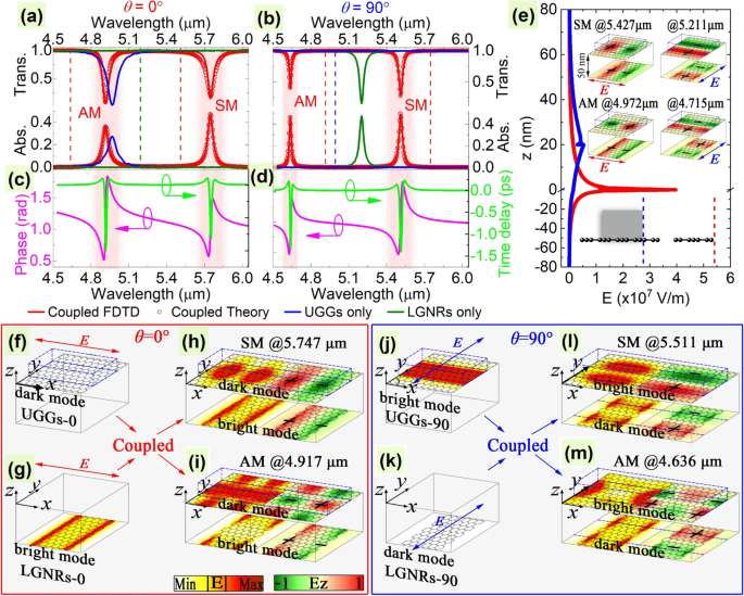
제안된 PIT 시스템의 메커니즘을 탐색하기 위해 그림 1에 표시된 구성의 수치 시뮬레이션이 계산되고 두 개의 서로 다른 편광 각도에 대한 해당 결과가 그림 2에 나와 있습니다. θ =0°일 때, 우리는 먼저 하부 그래핀 나노리본(LGNR)과 상부 유전체 격자가 장착된 그래핀이 단독으로 존재하는 상황에 대한 결과를 계산했습니다. 편광 방향이 LGNR에 수직이기 때문에 SP가 여기에서 여기되어 그림 2a에 표시된 파란색 선과 같이 5.327 μm에서 주요 흡수 피크가 생성될 수 있습니다. 대조적으로, 상부 그래핀 시트의 SP는 입사광이 유전체 격자에 평행하게 편광되기 때문에 이 편광 조건에서 여기될 수 없으며, 그 결과 그림 2a의 평평한 녹색 선에서 알 수 있듯이 강한 운동량 불일치가 발생합니다. 이러한 상황에서 그림 2g 및 f와 같이 LGNR의 직접 여기 모드와 UGG의 다크 모드를 각각 LGNRs-0 및 UGGs-0이라고 합니다. 그러나 여기서 흥미로운 점은 이 두 그래핀 층이 합쳐지고 충분히 가까워지면 5.747 μm와 4.917 μm에서 두 개의 흡수 피크(투과 딥)가 나타난다는 것입니다. 더 긴 공진 파장을 가진 하나는 47.16%에 도달하는 흡수에 의해 지배적인 반면, 더 짧은 공진 파장을 가진 다른 하나는 35.88%의 흡수 피크를 특징으로 하며, 이는 이 두 모드가 외부 입사광과 매우 강하게 상호 작용함을 나타냅니다. 이 두 모드는 두 공진기 간의 동위상 및 비위상 플라즈몬 결합에서 비롯됩니다. 특히 LGNR의 밝은 모드 공진은 입사광에 의해 직접 여기되기 때문에 고정 모드로 간주되어야 합니다. 그러나 상부 그래핀 층의 플라즈몬 공명은 직접 여기될 수 없지만 동위상 및 비위상 상호작용을 통해 LGNR에서 여기된 것과 결합할 수 있습니다. 이 PIT 효과를 직접적으로 초래하는 것은 2개의 공진기와 이들의 플라즈몬 커플링의 공존입니다. 두 모드의 기원 뒤에 있는 물리적 메커니즘을 명확하게 밝히기 위해 그림 2h와 i에서 이 두 모드에서 전계 분포를 표시합니다. E에 따르면 z 성분 필드 분포, 5.747 μm에서의 모드는 계층 구조의 동상 공진 특성을 나타내므로 대칭 모드라고 합니다. 4.917 μm의 모드는 역위상 공진을 나타내며 반대칭 모드라고 합니다. 게다가, 그림 2h와 i는 이러한 모드의 구조를 명확하게 보여줍니다. 모든 Ez 구성 요소는 2π를 특징으로 하는 쌍극자 모드 공진을 보여줍니다. 편광 방향을 따른 위상 변이(x 축) 각 그래핀 층에서. 이 두 가지 기본 모드는 LGNR의 공진 흡수를 제거하는 동시에 광학 스펙트럼에서 두드러진 투과 창과 두 개의 흡수 피크를 발생시켜 PIT(논의의 편의를 위해 이것을 LGNR-PIT라고 함)라는 광학 효과를 유발합니다. 그림 2c에서 두 개의 흡수 피크에서 전송 위상과 지연 시간을 표시합니다. 후자는 각각 0.34 ps 및 0.36 ps에 도달하여 시스템의 느린 조명 효과를 나타냅니다.
<그림>
전송 및 흡수 라인(a , b ) 및 전송 단계(왼쪽 y 축) 및 지연 시간(오른쪽 y 축) (c , d ) 편광 각도가 θ인 시스템 =0°(a , ㄷ ) 및 90°(b , d ), 각각. (a ) 및 (b ), 점선은 다른 편광에서의 공진 위치를 나타냅니다. (a에서 이론적으로 분석된 라인의 피팅 매개변수 ) 및 (b )는 (THz) 6.71, 110.07, 2.25, 0.46, 0.74이고 κ의 경우 5.73, 4.13, 72.83, 0.33, 0.27입니다. 나 , 질문1i /sqrt(ε0나1i ), 질문2i /sqrt(ε0나2i ), γ1i , 및 γ2i , 각각. UGG가 있는 경우의 전기장의 공간 분포(e (파란색 선), f , j ) 및 LGNR(e (빨간색 선), g , k) z만을 따라 축(e ) 및 해당 그래핀 평면(f , 지 , j , k ). 전기장의 공간 분포(왼쪽 패널) 및 해당 z 대칭 모드(SM)의 구성요소(오른쪽 패널)(h , @5.747 μm; 나 , @5.511 μm) 및 비대칭 모드(AM)(i , @4.917 μm; m , @4.636 μm) 편광 각도 θ에서 =0°(h , 나 ) 및 90°(l , m ), 각각. e의 상단 인서트 z 표시 d가 있는 경우의 전기장의 성분 =50 nm, 아래쪽 삽입물은 메인 플롯에서 필드의 위치를 나타냅니다. "+" 및 "-" 기호는 공명 표면 전하를 제공합니다. 더 어두운 색상은 더 큰 전하 밀도를 나타냅니다.
θ의 경우 =90°에서 SP는 5.202 μm의 주요 흡수 피크를 가진 UGG에서 여기될 수 있지만 그림 2b에 표시된 녹색 및 파란색 선과 같이 단독으로 존재할 때 LGNR에서는 여기될 수 없습니다. 이러한 상황에서 우리는 그림 2j 및 k에서와 같이 UGG의 직접 여기 모드와 LGNR의 다크 모드를 각각 LGNRs-90 및 UGGs-90으로 참조합니다. 그러나 이 두 모드가 서로 결합할 수 있을 만큼 가까우면 5.511 μm 및 4.636 μm에서 두 개의 투과 딥(흡수 피크)이 명확하게 나타나 흡수가 각각 49.07% 및 46.46%에 도달하므로 외부 입사파와의 상호 작용이 θ의 경우와 유사하며 Fig. 2b와 Table 1과 같이 매우 강력하다. =0°일 때, 물리적 메커니즘은 두 그래핀 층 사이의 동위상 및 비위상 플라즈몬 커플링을 고려하여 이해할 수도 있습니다. 그림 2l과 m에서 명확히 알 수 있듯이 Ez 구성 요소 필드 분포는 2πy에 따른 위상 변이 각 그래핀 층의 축을 확인하고 해당 흡수 피크에서 동위상(대칭 모드) 및 역위상(반대칭 모드) 공명을 나타냅니다. UGG만으로 케이스의 공진 흡수를 제거하는 동시에 광학 스펙트럼에서 두드러진 투과 창과 두 개의 흡수 피크를 생성하여 또 다른 PIT를 생성하는 것은 이 두 가지 기본 모드입니다(논의의 편의를 위해 이것을 UGGs-PIT라고 합니다. ). 그림 2d에는 두 흡수 피크에서의 투과 위상과 지연 시간도 표시되어 있으며 대칭 모드와 비대칭 모드에서 각각 0.23 ps 및 0.21 ps의 피크 값으로 느린 광 전파 효과를 보여줍니다.
그러나 그림 2i 및 m에서 비대칭 모드의 상부 그래핀 시트의 필드 분포가 "다극" 공진 모양을 보여주지만 전하 진동도 특성을 유지하기 때문에 여전히 쌍극자 모드입니다. 편광 방향을 따른 쌍극자 모드 공진. "다극" 공진 모양의 이유는 LGNR의 강한 필드 간섭 때문입니다. 이는 그림 2e와 같이 패턴화된 GNR에서 가장 강한 국부 플라즈몬 필드가 연속 그래핀 시트[60]보다 더 뚜렷하다는 사실을 고려하여 이해할 수 있습니다. 이러한 "다극" 모드 모양은 필드 모니터를 두 개의 그래핀 층에서 설정하거나 큰 결합 거리를 사용하면 사라집니다(예:d). =50 nm에서 "다극" 모드 모양은 그림 2e의 삽입물에서 볼 수 있듯이 순수한 쌍극자 모드 공진으로 변경됩니다. 게다가, 우리는 또한 두 그래핀 층 사이의 모드 커플링이 다르다는 것을 주목합니다. 특히, θ의 경우 =0°, LGNRs-PIT는 x를 따라 공진하는 LGNRs-0과 UGGs-0 사이의 강한 결합의 결과입니다. 방향. θ의 경우 =90°, UGGs-PIT는 y를 따라 공진하는 UGGs-90과 LGNRs-90 사이의 강력한 결합의 결과입니다. 따라서, LGNRs-PIT 및 UGGs-PIT는 서로 다른 극성에서 공명하는 서로 다른 모드 간의 플라즈몬 결합 효과로 두 가지 서로 다른 PIT 효과가 발생합니다.
따라서 그림 2에서 LGNRs-PIT(θ 포함)라는 결론을 내릴 수 있습니다. =0°) 및 UGGs-PIT(θ 포함) =90°)는 2개의 서로 다른 PIT 효과로, 계층화된 그래핀 시스템의 두 개의 별도의 밝은 모드에서 어두운 모드로의 커플링 경로로 인해 발생하며 다른 스펙트럼 응답으로 표시됩니다. 즉, 편광에 둔감한 PIT 효과와 매우 다른 입사광의 편광 방향을 변경하는 것만으로 이 두 PIT 효과를 서로 전환할 수 있습니다(토론 부분 참조). 게다가, 이 전환 가능한 PIT 효과는 Eqs에 표시된 2-입자 모델로 설명할 수 있습니다. (1) 및 (2). θ의 경우 =0°일 때 UGG의 입사 필드에 대한 직접 결합 효율은 0(어두움)인 반면 LGNR의 효율은 방정식의 오른쪽에서 알 수 있듯이 가장 높은(밝음)입니다. θ의 경우 =90°, 그 반대의 경우 UGG는 밝아지고 LGNR은 어두워집니다. 두 경우 모두 Eq.로 얻은 분석 결과 사이의 일치에 유의하십시오. (5)(그림 2a, b에서 빨간색 원으로 표시) 및 수치 결과(그림 2a, b에서 빨간색 선으로 표시)는 거의 완벽합니다. 우리의 분석 모델은 그림 2에서 볼 수 있듯이 공진의 위치뿐만 아니라 피크 값도 매우 정확하게 예측합니다. 마지막으로 여기에 제시된 결과는 동일한 공진기 [35, 38]; 이는 서로 다른 편광에서 그림 2와 같은 결과를 얻을 수 없기 때문입니다. 차이점은 토론 부분에서 더 논의하겠습니다.
PIT의 기하학적 조정 가능성
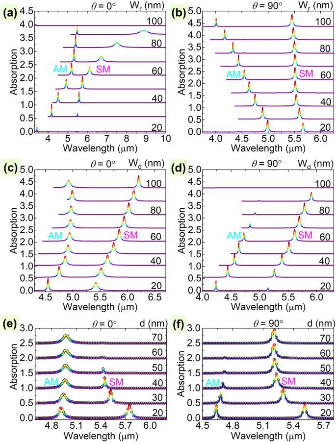
우리는 밝은 모드와 어두운 모드 사이의 근거리 커플링이 두 가지 편광 종속 PIT 효과를 초래한다는 것을 입증했습니다. 따라서 밝은 모드와 어두운 모드 공명에 큰 영향을 미치는 매개변수와 이들 간의 결합 강도는 PIT 효과에 대한 조정 가능한 매개변수로 처리될 수 있습니다. 먼저 θ의 경우에 대한 매개변수 연구를 수행합니다. =너비를 변경하여 0°(Wr ) LGNR 및 너비(Wd ) 20 ~ 100 nm의 UGG의 결과를 각각 그림 3a와 c에 보여줍니다. LGNR은 입사광과 직접 결합하고 이러한 조건에서 밝은 모드로 작동하기 때문에 크기가 변경되면 시스템의 전체 플라즈몬 응답에 직접적인 영향을 미칩니다. 예를 들어, Wr 20 nm와 같이 매우 작으면 GNR의 낮은 점유율로 인해 입사광과의 결합 효율이 매우 약해 [14, 51] PIT 시스템의 대칭 모드, 특히 대칭 모드의 흡수가 낮습니다. W의 흡수선에서 알 수 있듯이 r =그림 3a에서 20 nm. 다른 예로, Wr 충분히 크고 특히 최대 100 nm에 도달하면(즉, LGNR이 전체 그래핀 층일 때) 두 공진기 중 어느 것도 외부 필드와 결합할 수 없으므로 LNGRs-PIT가 사라집니다. 특히, 두 모드의 흡수는 W일 때 동시에 가장 높은 값을 나타냅니다. r 약 50 nm이다. 밝은 모드와 달리 DG 너비의 변화(Wd ) 다크 모드에 대한 상부 그래핀 층은 공진 위치와 대칭 모드 및 비대칭 모드의 흡수를 한계 내에서 조정할 수 있는 반면, 그림 4에서와 같이 외부 파동과의 높은 결합 효율을 제거하거나 크게 영향을 미칠 수는 없습니다. 3c. 실제로 유전체 격자가 제거되거나 전체 유전체층이 되어도(Wd =100 nm), LGNR은 하나의 PIT 효과만 존재하도록 허용되는 이전 연구[36]에서 설명된 2차원 사례에 의해 입증되었듯이 여전히 상부 그래핀 시트와 결합할 수 있습니다.
<그림>
(a ), (b ) 리본 너비 Wr LGNR의; (ㄷ , d ) DG 너비 Wd UGG의; 그리고 (e , f ) 이격 거리 dθ의 편광각에서 10/20 nm의 간격으로 두 그래핀 층 사이 =0°(a , ㄷ , e ) 및 90°(b , d , f ), 각각. (a –f ), 실선의 짙은 붉은색은 더 강한 흡수를 나타냅니다. 일부 선은 다른 고차 흡수 피크로부터 주의가 산만해지는 것을 피하기 위해 잘렸습니다. (e에서 ) 및 (f ), 실선 및 다크 서클은 각각 수치 및 이론 결과를 나타냅니다. SM과 AM은 각각 대칭 모드와 비대칭 모드를 나타냅니다.
그러나 θ의 경우 =90°, 결과는 θ의 경우와 대조됩니다. LGNR은 어두운 모드로 작동하고 UGG는 밝은 모드로 작동하기 때문에 =0°입니다. 구체적으로 LGNR 폭 W의 변화 r 그림 3b와 같이 대칭 모드와 반대칭 모드의 공진 위치와 최대 흡수만 변조하는 반면 두 모드의 존재를 소멸시킬 수는 없습니다. 이는 LGNR이 이러한 편광 조건에서 다크 모드로 동작하기 때문이다. W가 있는 조건에서 r =100 nm, 시스템은 다른 연구에서 이전에 보고된 2차원 단일 PIT 시스템과 유사한 다른 그래핀 시트와 결합하는 DG 로딩된 그래핀 시트가 됩니다[34]. 그러나 이 조건에서 상부 그래핀 시트가 밝은 모드로 작동하기 때문에 상부 유전체 격자의 변경은 PIT 시스템의 광학 응답에 큰 영향을 미치며 이는 W를 변경할 때와 매우 유사합니다. rθ와 함께 =0°, 그림 3d에 표시된 대로. 일반적으로 우리는 그림 3a-d에서 밝은 모드의 조정이 그림 3a와 d에서 보여지는 것처럼 UGGs-PIT의 외관과 존재에 큰 영향을 미칠 것이라는 결론을 내릴 수 있습니다. 어두운 모드는 그림 3b와 c와 같이 UGGs-PIT에서 대칭 모드와 비대칭 모드의 공진 위치와 상대적 강도만 변경할 수 있습니다.
PIT 효과에 큰 영향을 미치는 또 다른 매개변수는 공백 d입니다. 두 그래핀 공진기 사이 GNR과 유전체 격자의 너비를 고정한 다음 d를 늘립니다. , the interaction strength between the two graphene resonators decreases monotonically for both polarization angles due to the fast decreasing plasmonic field in the normal direction of the graphene surface [35, 61]. As a result, the symmetric mode and the antisymmetric mode are respectively extinguished for the case with θ =0° and θ =90° at large coupling distance, e.g., d> 70 nm, as shown in Fig. 3e and f. As it is known that when the bright and dark modes are far beyond the decay length of the evanescent field of each other, these two modes are uncoupled, and therefore, only the bright mode exists. At that point, we can conclude from Fig. 3e and f that the symmetric mode and antisymmetric mode of the PIT respectively originate from the UGGs and LGNRs, as they remain at large layer distance. Note that the PIT effects at different coupling strengths match well with the two-particle model, as the simulated and analytically predicted results are in excellent agreement, as can be seen in Fig. 3a and b, where the solid curves are gotten from FDTD, and the dark circles are from the two-particle model.
Electrical Tunability of PIT
One of the major advantages of graphene-based plasmonic devices is their dynamic and broadband tunability, which can be realized by electrostatic gating techniques [61, 62]. This intriguing property allows us to electrically change the Fermi energy of graphene and, thus, to actively modulate the transmission window of the proposed PIT systems to work at different wavelengths without reconstructing the geometrical structure [24, 25]. By applying different bias voltages with a field-effect transistor structure, researchers have experimentally achieved the dynamical tune of the Fermi energy level from 0.2 to 1.2 eV [63]. The simulated absorption spectra shown in Fig. 4 confirms the broadband and dynamic tunability of the proposed PIT device. For the given geometrical parameters, the plasmon wavelengths of the symmetric mode and antisymmetric mode of the LGNRs-PIT (UGGs-PIT) can be tuned from 4.977 to 9.953 μm and 4.259 to 8.520 μm (from 4.775 to 9.551 μm and 4.015 to 8.033 μm) when the Fermi level is modulated from 0.8 to 0.2 eV, respectively, as the solid and dash-dotted lines shown in Fig. 4a and b. This dynamic tunability will greatly facilitate the design and practical application of the proposed PIT device.
Absorption spectra of the symmetric mode (solid lines) and antisymmetric mode (dash-dotted lines) of the proposed PIT system with different Fermi energy levels of graphene at polarization angles of θ =0° (a ) and 90° (b ), 각각
Applications
In the previous parts, we have made clear how the LGNRs couple with the UGGs and further result in the polarization-dependent PIT effects, and demonstrated how the geometrical and electrical parameters affect the couplings. In this part, we will demonstrate our proposal can be used as selective refractive index sensors and dual-band perfect absorbers.
Considering that the PIT effect is determined by both the bright and dark mode resonances, what brings the change to these two modes will directly alter the symmetric mode and antisymmetric mode in the PIT window. Therefore, the induced symmetric mode and antisymmetric mode are highly sensitive to the local dielectric environment, which can be applied to design refractive index sensors [64]. In our design, both the regions above the UGGs (with refractive index n0 ) and below the LGNRs (with refractive index n2 ) can be thought of as the sensing regions. To calculate the sensitivities, we define S =Δλ/ Δn , which specifies the plasmon wavelength (λ ) shift per refractive index unit (RIU). We assume the refractive indexes of the materials as n1 =2.0 and n0 =n2 =n3 =1.3 (except the cases when n0 or n2 is working as the sensing regions with the range changing from 1.0 to 1.1).
Firstly, when tuning the width of the GNRs (Wr ), we find that when the sensing region is alongside the bright mode (that are sensing region n0 with θ =90° and sensing region n2 with θ =0°), the sensitivity of the symmetric mode SSM gets bigger at wider ribbon width (see the solid blue lines in Fig. 5b, c). Especially, SSM can reach 4 μm/RIU for the case with θ =0° in sensing region n2 . Secondly, for the case with increasing DG width (Wd ), both the sensitivity of the symmetric mode SSM and antisymmetric mode SAM decrease in most cases. Finally, as for the coupling distance d between the two layers, it is found that SSM decreases while that of the antisymmetric mode increases for both of the polarization angles (see the solid and dash-dotted dark lines in Fig. 5). Considering that the antisymmetric mode will disappear under large coupling distance at the polarization angle of θ =90° (see Fig. 3f), the antisymmetric mode for the situation with θ =0° is more suitable to work as a sensor at a larger distance. Generally, the sensitivities of the symmetric mode and antisymmetric mode of the LGNRs-PIT and UGGs-PIT are respectively comparable to each other, as can be concluded by comparing Fig. 5a with 5b, and Fig. 5c with 5d, respectively. Besides, it is also found that the sensitivities for the cases with sensing regions alongside the bright and dark modes do not show a big difference, as can be seen by comparing Fig. 5a with 5d (alongside the dark mode), and Fig. 5b with 5c (alongside the bright mode). However, the sensitivities of the case with the sensing region under the LGNRs are obviously higher than that of the case with the sensing region above the UGGs, as they are shown by comparing Fig. 5a and b with Fig. 5c and d. This is because the sensitivity is directly related to the localized plasmonic field [64], and the local plasmonic field in the cutting-edge nanoribbons is generally stronger than the continuous edge-free graphene dielectric gratings [60].
Refractive index sensitivities of the symmetric mode (SSM , solid lines) and antisymmetric mode (SAM , dash-dotted lines) in the sensing regions of n0 (아 , b ) 및 n2 (ㄷ , d ) as functions of the ribbon width Wr of LGNRs, the DG width Wd of UGGs, and the separation distance d between the two graphene layers at polarization angles of θ =0° (a , ㄷ ) and 90° (b , d ), 각각. The inserts show the location of the sensing region
Besides working as a refractive index sensor, the proposed system can also be further designed as a perfect absorber. To achieve this, we can add a metallic substrate below the LGNRs and assume the refractive indexes of the materials as n1 =2.0 and n0 =n2 =n3 =1.3. With the existence of the metallic substrate, the dielectric layer between the LGNRs and metallic mirror forms a Fabry-Perot cavity, which can increase the interaction of incidence with graphene layers and further increase the absorptivity of the two modes. For the LGNRs-PIT case with θ =0°, we find that perfect absorptions with absorptivity> 96% of the symmetric mode and antisymmetric mode can be achieved simultaneously when the metallic substrate is with a 3.0-μm distance below the LGNRs, as shown in Fig. 6a and c. We also find that our proposal has good robustness to the doping level of graphene, as shown in Fig. 6a. The absorptivity of the two modes is> 90% when the Fermi energy level of graphene ranges from 0.58 to 0.66 eV. Besides the doping level of graphene, the perfect absorptions also show good tolerance to the polarization angle:The absorptivity of the two modes can keep at a high level (>90%) even the polarization angle ranges from − 17 to 17°. The robustness to the parameters is good for the practical design of the absorber.
Absorption spectra with different Fermi energy levels of graphene at polarization angles of θ =0° (a ) and 90° (b ) for the cases with a metal substrate below the LGNRs with a distance of 3.0 μm (a , ㄷ ) and 1.2 μm (b , d ), 각각. (ㄷ , d ) Absorption maxima as functions of θ . SM and AM refer to the symmetric mode and antisymmetric mode, respectively
To achieve the perfect absorption for the UGGs-PIT case with θ =90°, we need to set the metallic substrate with a 1.2-μm distance below the LGNRs. It is found that perfect absorptions with absorptivity> 95% of the symmetric mode and antisymmetric mode can be achieved simultaneously, as shown in Fig. 6b and d. Similar to the LGNRs-PIT case, it also found that the perfect absorptions show good tolerance to the polarization angle ranging from − 15 to 15° with absorptivity of the two modes> 90% (see Fig. 6d). More notably, the proposed absorber for the UGGs-PIT case shows much bigger robustness to the doping level of graphene, as plotted in Fig. 6b. It is found that the absorptivity of the two modes is> 90% even the Fermi energy level of graphene ranges from 0.55 to 1.15 eV. Considering that the Fermi level of graphene can be dynamically tuned by an external gate voltage, the designed structure can be thought of as active dual-band perfect absorber with a working wavelength of the symmetric mode (antisymmetric mode) ranging from 4.59 to 6.64 μm (3.77 to 5.45 μm).
Discussions
In this part, we discuss the advantages and differences of the proposed structure with other similar structures. To this end, we first calculated the plasmon resonant wavelengths for the cases with only the GNRs and only the dielectric grating-loaded graphene, as shown in Fig. 7a. It shows that the plasmon wavelengths have different dependencies on the width of the resonator. Besides, the inserts show the resonant property of the modes:For GNRs, the plasmonic fields are mainly localized on the edge of the GNR, while for the case with graphene sheet attached with dielectric gratings, the plasmonic fields are mainly concentrated on the grating area. Previous studies have shown that the field distributions and the distance between the resonators will greatly affect the plasmonic couplings [35, 65] and, therefore, the spectral response of the coupled system. That is to say, in our cases, the couplings from the LGNRs to the upper dielectric gratings are different from the other way coupled from the upper dielectric gratings to the LGNRs. Therefore, we obtain the results shown in Fig. 7b that even when the plasmon wavelengths of the two resonators are the same when they exist alone, they will also lead to two distinct PIT effects no matter what they work as bright or dark modes. To show more clearly the advantage of our design, we plot the resonant mode positions of the PIT effects for different geometrical parameters in Fig. 7c and d. They clearly demonstrate that there are always two distinguishable PIT effects for the two polarization directions, even when the geometrical parameters are the same.
(아 ) Plasmon wavelengths of the cases with only the GNRs and only dielectric grating-loaded graphene sheet for different ribbon and grating width. The inserts show the field distribution of the modes. (b ) Absorption spectra for different polarization angles of GNR and dielectric grating-loaded graphene-coupled system with their width of 54 nm. (ㄷ –f ) Resonant positions of the two PIT peaks at different polarization angles for different systems. The inserts show the corresponding structures
However, one may want to know why the proposed structure is not designed with the same resonators, such as perpendicular GNRs and dielectric grating-loaded graphene, as it has been reported in the previous studies [35, 38]. To explain this, we have plotted the resonant positions of the two modes in the PIT effects for the structures with pure GNRs and dielectric grating-loaded graphene resonators in Fig. 7e and f, respectively. It is found that when the two layers of resonators are designed with the same geometrical parameters, there is only one PIT effect for all the polarization directions, which means the PIT effect becomes indistinguishable from the absorption spectrum. This is because the couplings between the two layers of resonators are equivalent due to the same field distribution of the plasmon modes. That is to say, the polarization-independent PIT effects of the structures shown in the insert of Fig. 7e and f depend on the particular choice of the geometrical parameters. Whereas, on the contrary, the design in this paper to achieve two switchable PIT effects is not dependent on the particular choice of the geometrical parameters, which can guarantee the existence of the two switchable PIT effects.
결론
In this paper, both advanced simulations and theoretical analyses are combined to investigate switchable PIT effects in two graphene layers formed by GNRs coupled with a dielectric grating-loaded graphene layer. Thanks to the crossed nanoribbon and grating directions, both the GNRs and the dielectric gratings can operate as either the bright or the dark mode depending on the polarization direction. The incident light under these two polarization directions introduces two different bright to dark mode coupling pathways within the two resonators, resulting in two switchable PIT effects. Geometrical parameters, such as graphene nanoribbon width, dielectric grating width, layer distance, and graphene Fermi level, are used to study the physical mechanism and the performance of the proposed PIT effect. Additionally, the proposed concepts are examined by applying a two-particle model, showing outstanding agreement with the numerical results. The proposed methods provide a general approach to achieving switchable PIT effects in distinct resonator-coupled system and can advance the applicability and versatility of PIT-based plasmonic sensing platforms and active dual-band perfect absorbers.