연마 흐름 연마는 현대의 초정밀 가공에서 중요한 역할을 합니다. 연마재 흐름의 매질에 부유하는 초미세 입자는 나노 스케일로 물질을 제거합니다. 이 논문에서는 연마 흐름 연마 중 연마 절단 공정에 대한 충격 방향의 영향을 조사하기 위해 3차원 분자 역학(MD) 시뮬레이션을 수행했습니다. 분자 역학 시뮬레이션 소프트웨어 Lammps는 다양한 절단 각도(0
o
)에서 SiC 연마 입자가 있는 단결정 구리의 절단을 시뮬레이션하는 데 사용되었습니다. –45
o
). 일정한 마찰 계수에서 절삭 각도와 절삭력 사이의 직접적인 관계를 발견했으며, 이는 궁극적으로 연마 흐름 가공 중 전위 수를 증가시킵니다. 우리의 이론적 연구는 작은 절단 각도가 표면 품질을 개선하고 공작물의 내부 결함을 줄이는 데 도움이 된다는 것을 보여줍니다. 그러나 절단 각도와 마찰 계수 사이에는 명확한 관계가 없습니다.
<섹션 데이터-제목="배경">
배경
현대의 초정밀 가공에서 재료 제거 기술은 마이크로일렉트로닉스, 마이크로기계 및 광학 요소 제조에서 중요한 역할을 합니다. 높은 치수 정확도와 품질 표면을 가진 소형 장치에 대한 요구로 인해 언급된 분야에서 초정밀 공정이 주요 선택이 되었습니다[1]. 또한, 표면 구성 요소와 표면 아래 구조의 변화는 나노미터 길이 규모입니다. 연마 입자 흐름 연마 기술은 정밀 가공의 많은 분야에서 중요한 역할을 하며 표면 품질을 향상시키는 다른 비 전통적인 마무리 기술과 같습니다. 이 기술은 중요한 역할로 인해 많은 연구자를 끌어들였습니다. E. Uhlmann과 다른 연구원들은 절삭 재료의 영향에 대한 다양한 가공 요소의 연삭 유체 흐름을 확인하기 위해 설계된 실험을 위해 연마 입자 연마 세라믹 표면의 컴퓨터 시뮬레이션을 보고했습니다[2]. Sehijpal Singh와 다른 연구원들은 구리 및 알루미늄 재료를 절단하기 위해 연마 흐름 연마 기술을 사용합니다. 주사 전자 현미경 분석에서 그들은 작업물의 깊은 홈 표면을 발견했습니다[3]. G. Venkatesh와 다른 연구원들은 마무리 공정의 복잡한 표면에 있는 원추형 기어에 대한 초음파 보조 연마 입자 연마 기술을 보고했습니다. 이 기술에서는 연마 입자 속도가 기존 연마 입자 흐름보다 빨라서 공작물의 표면과 충돌하여 처리 효율을 향상시킬 수 있습니다. 실험적이고 이론적인 방법에서 그들은 이 기술이 기어 블레이드 마무리를 위한 최선의 선택 중 하나라는 것을 발견했습니다[4, 5]. K. Kamal et al. 유체 연마제 점도, 전단 속도 및 크리프 시간에서 연마액의 유변학적 특성을 연구했습니다[6]. 그러나 대부분의 연마 흐름 연마 연구는 거시적 수준을 기반으로 하며 매우 드물게 미시적 수준에 주의를 기울였습니다. 연마 흐름 연마 공정에서 매체의 부유 입자는 미세 절단 공작물 표면의 영향으로 특정 속도로 매체를 따라 흐릅니다(그림 1).
<그림>
연마 절단 공작물의 스케치입니다. 모든 수치는 분자 역학을 이용한 연마 나노미터 절단 공정에 대한 영향 방향의 영향에 관한 것입니다. 그림 1은 연마 절단 공작물의 스케치입니다. 연마 흐름 연마 공정에서 매체의 부유 입자는 미세 절단 공작물 표면의 영향으로 매체를 따라 특정 속도로 흐릅니다.
연마 입자의 모양이 규칙적이지 않기 때문에 도구와 유사하게 공작물의 표면에 작용하는 특정 모서리와 모서리가 있습니다. 그러나 절단 공정은 원자 규모로 재료 제거 공정과 분명히 다릅니다. 나노 스케일 절단은 재료 표면의 수 나노미터 이하를 포함하지만 이 과정을 실험으로 관찰하는 것은 매우 어렵습니다. 따라서 이론적 조사 방법인 MD 시뮬레이션은 나노미터 절단 공정을 연구하는 데 매우 유용합니다. 조건 예측 및 분석을 위해 원자의 상호 관계를 연구하기 위해 시간 기반 통계 역학 방법을 사용하는 컴퓨터 시뮬레이션 기술로서의 분자 역학. 이것은 또한 재료 제거 프로세스를 시뮬레이션하고 이해하기 위한 강력한 도구입니다. 문헌에는 정밀 가공을 조사하기 위한 도구로서 MD에 관한 많은 연구가 있습니다. Oluwajobi와 Chen은 구리 나노 스케일 가공의 MD 시뮬레이션에 대한 광범위한 작업을 수행했습니다[7]. 그들의 연구에서 그들은 최소 절단 깊이, 기하학 및 원자 간 전위와 같은 나노 가공에 대한 다양한 매개 변수를 조사했습니다[8]. 또한 MD 시뮬레이션 결과는 실리콘과 같은 취성 재료의 나노미터 절단 공정과 관련된 많은 문제를 해결하기 위해 과거에도 성공적이었습니다[9]. Komanduriet al. Tersoff 전위를 사용하여 결함이 없는 순수 실리콘 단결정의 나노미터 절단을 위한 MD 시뮬레이션을 수행했습니다. 그들은 재료 제거 및 표면 생성에 대한 경사각, 절단 폭, 절단 깊이 및 여유각의 영향을 연구했습니다[10]. Goel et al. 나노미터 절단 과정에서 SiC의 연성 응답의 원자적 측면을 조사했습니다. 그들은 sp3-sp2 질서-무질서 전이의 존재를 발견하여 마침내 다이아몬드의 흑연화를 초래했습니다[11]. Cai et al. 실리콘의 나노 스케일 연성 모드 절단을 연구하기 위해 MD를 사용했습니다. 그들은 공구 절삭날과 공작물 재료의 전단 응력에 미치는 영향을 보고했습니다[12]. Arafin et al. 실리콘 웨이퍼의 나노스케일 연성 모드 절단에서 절삭날 반경의 영향에 대해 논의했습니다[13]. 다양한 다른 연구자들도 MD 시뮬레이션을 사용하여 실리콘 나노 가공의 다양한 조건을 강조했습니다. 절삭력, 절삭 깊이, 온도, 전단 응력 및 기타 매개변수로 조사가 이루어집니다. 그러나 이 분야에서 적절한 실험적 검증이 부족합니다. Qihong Fang et al. 스케일이 다른 서로 다른 이종 재료에서 전위의 상호 작용 메커니즘, 전위 및 재료 인성과 파괴 손상 사이의 관계를 연구했습니다. 그들은 분자 역학 시뮬레이션을 사용하여 단결정, 다결정 및 나노쌍정 다결정 구리를 포함한 세 가지 다른 결정 구조에 대한 나노인덴테이션을 연구합니다. Scratch rate의 증가에 따라 심한 소성변형과 큰 chip volume으로 인해 Scratching력과 가공물 온도가 지속적으로 상승하여 dislocation slip, GB slip, twining/detwining이 발생한다[14, 15].
방법/실험
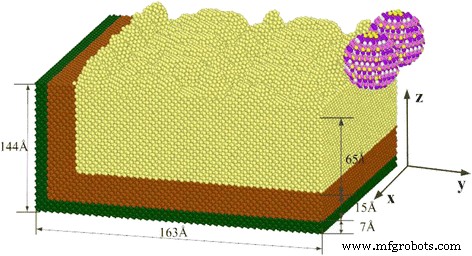
연마 흐름 연마 실험에서 공작물은 일반적으로 SiC 연마재로 절단되었습니다. SiC 연마 입자의 모델이 확립된 후, 소프트웨어 Lammps에 의해 공작물의 분자 역학 시뮬레이션이 수행되었습니다. 각도가 다른 두 개의 SiC 연마 절단 단결정 구리 모델을 구성했습니다. SiC 연마 입자 충돌 절단 단결정 구리의 시뮬레이션 모델이 그림 2에 나와 있습니다.
<그림>
SiC 연마 단결정 구리 절단 시뮬레이션 모델. 그림 2는 SiC 연마 절단 단결정 구리의 시뮬레이션 모델에 관한 것입니다. 우리는 단결정 구리를 절단하기 위해 두 개의 SiC 연마재를 만들었습니다. 연마 흐름 연마 실험에서 공작물은 일반적으로 SiC 연마재로 절단되었습니다. SiC 연마 모델 구축 후, 공작물의 분자 역학 시뮬레이션이 수행되었습니다. 각도가 다른 두 개의 SiC 연마 절단 단결정 구리 모델을 구축했습니다.
시뮬레이션된 원자의 수는 159,020개이고 모델의 크기는 그림 2에 나와 있습니다. 연마반경은 15Å, 연마입자의 총 C 원자수와 Si 원자수는 1406개, 탄소수는 681개, 규소수는 725개였다. 완화 단계 수는 시뮬레이션된 평형 앙상블에 대해 10,000 단계로 설정되고 충돌 시뮬레이션 단계는 100,000 절단 단계로 설정되고 시뮬레이션의 각 단계는 0.001ps, 절단 시뮬레이션, 절단 방향 속도 80m/s의 SiC 연마 입자. AFM 분석 값 입자는 연마 중에 미세 가공 공작물과 충돌하고, SiC 연마 입자는 분자 충돌 역학 다른 각도 절단 공정을 탐색합니다. 연마 흐름 절단 과정에서 절단 속도가 증가함에 따라 절단력이 증가하고 절단력의 크기는 절단 효과에 직접적인 영향을 미칩니다. 따라서 적절한 절단 속도의 선택은 절단 품질에 중요한 영향을 미칩니다. 고품질 절단을 달성하기 위해 80m/s의 절단 속도를 선택했습니다. 절단 속도가 공작물 원자 사이의 상호 작용을 빠르게 파괴할 수 있는 절단력을 생성하기 때문입니다[16].
10 m/s와 같은 낮은 절단 속도에서 분자 역학 시뮬레이션에서 원자 변위 맵과 실리콘 카바이드 연마 입자의 절단력 및 절단 각도가 시뮬레이션 단계 크기에 따라 어떻게 변하는지 패턴이 그림 1과 그림 2에 나와 있습니다. 3, 4. 절삭 속도가 너무 느리기 때문에 절삭력도 불충분하여 격자의 변형 및 전위가 훨씬 적습니다. 전체적으로 절단 효율이 낮고 절단 품질이 상대적으로 열악합니다. 대조적으로, 현미경 실험에서 절단 속도가 최대 80m/s일 때 구리 원자 사이의 화학 결합이 빠르고 효과적으로 끊어질 수 있으므로 즉각적인 고품질 절단의 목표를 달성할 수 있습니다. 따라서 종합적인 분석을 거친 후 80m/s의 절삭 속도가 시뮬레이션에 적합합니다.
<그림>
저속 원자 변위
<그림>
절삭력, 절삭각 및 시뮬레이션 단계 간의 관계
타당성과 신뢰성을 시뮬레이션하기 위해 우리는 원자의 원자간 전위를 고려하는 합리적인 경험적 전위 함수를 선택합니다. 다른 대상에 따라 전위 기능을 쌍 전위 기능과 다체 전위 기능으로 나눌 수 있습니다. 단결정 구리와 연마 입자 사이의 두 모델은 모스 전위에 의해 그들 사이의 원자간 전위를 설명하고[17], EAM 전위는 구리 원자 사이 원자의 원자간 전위를 설명하는 데 사용됩니다[18,19,20]. SiC 입자 간의 상호 작용은 Tersoff 전위를 사용하여 설명됩니다[21].
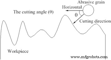
연마 과정에서 매체에서 연마 입자의 충돌 방향은 무작위입니다. 궤적이 공작물의 표면을 따라 정확히 일치하지 않습니다. 미세 절단 공정 중에 연마 입자의 절단 방향이 항상 공작물 재료에 수직인 것은 아닙니다. 절단각은 연마입자의 절단방향과 수평면이 이루는 각도를 의미한다. 입자가 공작물 표면을 향해 접근하면 양수입니다. 절단 각도의 스케치는 그림 5에 나와 있습니다.
<그림>
절단 각도의 스케치입니다. 그림 5는 연마 입자가 절단될 때 다양한 절단 각도의 스케치입니다. 공작물 재료를 절단하는 다른 방향의 연마 입자, 재료의 성능 및 가공 품질이 달라집니다.
이 연구에서는 절단 단결정 구리의 영향 방향이 다른 다중 연마재를 시뮬레이션하기 위해 MD 시뮬레이션이 사용되었습니다. 그림 5에서 볼 수 있듯이 절삭각은 0°~45° 사이이며 구리 가공물의 표면은 거칠다.
결과 및 토론
SiC 연마 절단 역학 충돌 분석
단결정 구리 재료의 절단에 대한 탄화규소 연마제의 영향은 구리 재료의 단결정 격자 구조를 파괴함으로써 달성됩니다. 파괴 과정에서 구리 원자 사이의 상호 작용, 피삭재의 Cu 원자에 대한 SiC 연마 입자의 C, Si 원자에 의한 전단 응력이 절삭력으로 확인되었으며, 이는 절삭력의 중요한 물리적 매개변수입니다. 단결정 구리 공작물 재료의 제거 과정을 깊이 반영합니다. 앞서 논의한 바와 같이 마이크로 절삭력과 매크로 절삭력 사이에는 큰 차이가 있습니다. 일반적으로 거시절삭력은 절삭력과 연삭력의 합이고, 미세절삭은 지립과 피삭재 원자의 상호작용에 의해 절삭력이 발생한다.
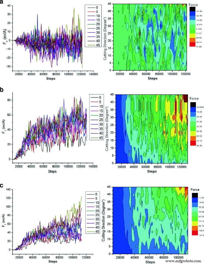
Fig. 6은 다양한 방향에 따른 연마입자의 전단응력 변화, 다양한 방향에 따른 전단응력의 영향, 절삭각도에 따른 절삭력 분포를 보여주고 있다.
<그림>
절삭 각도와 시뮬레이션 단계 크기가 절삭력에 미치는 영향. 그림 6은 SiC 연마 절삭력과 절삭 각도 및 시뮬레이션 단계 다이어그램을 보여줍니다. 절삭 깊이가 증가함에 따라 파괴 결정 구조의 수가 증가하고 절삭력 변동의 최대 값도 커집니다. 아 절삭력의 방향. ㄴ 절삭력의 방향. ㄷ [001] 절삭력 방향
탄화규소 연마 입자는 [010] 및 [100]과 같은 다른 각도의 모서리에서 단결정 구리 재료에 절단 및 충격을 가합니다. [001] 및 [010] 방향에 따른 절삭력은 전단력이었다. 추가 시뮬레이션에서 절삭 깊이가 점차 증가하여 [001] 및 [010] 방향을 따라 절삭 부하가 지속적으로 증가했습니다. 그러나 특정 한계까지 이러한 힘은 그림 6에서 볼 수 있듯이 변동했습니다. 연마 입자가 공작물의 재료 쪽으로 이동하면 가장 바깥쪽의 구리 원자와 원자 사이의 상호 작용(인력에서 반발로)이 완전히 변경되었습니다. SiC(Si 및 C). 초기에는 피삭재를 연삭할 때 구리 원자의 반발력으로 인해 절삭력이 부족했습니다. 마무리 공정의 경우 연마 입자가 구리 원자의 화학 결합을 쉽게 끊고 자유롭게 움직일 수 있도록 절삭력이 충분히 높아야 합니다. 또한 절삭 깊이 증가는 원자 상호 작용과 직접적인 관계가 있습니다. 원자가 쌓이기 시작하면 연마 입자가 공작물에 들어갈 때까지 절삭력이 지속적으로 증가하므로 정상 상태의 절삭력이 필요합니다. 이 상대적으로 안정적인 단계에서 절삭력 변동은 격자 변형 정도, 격자 재구성, 비정질 위상 변화 및 칩 생성의 영향을 받습니다. 연마 입자가 절단 방향을 따라 이동함에 따라 FCC 격자의 구리 원자에 외력이 가해져 구리 원자의 변위가 발생했습니다. 이 변위는 FCC 격자를 붕괴시키고 전위를 갖는 새로운 격자 구조로 변형시킨다. 절삭력에서도 유사한 상황이 관찰됩니다. [010] 방향을 따른 절단력과 입자의 충돌 각도 사이에는 양의 선형 상관 관계가 없습니다. 0°, 5°, 10° 이상의 충돌에서 [010] 방향의 힘은 다른 절단 방향의 힘보다 작고 변동이 적습니다. 더 작은 각도로 절단하면 3.5 ~ 15 Å의 높이 범위에서 버를 정의할 수 있으므로 기본적으로 버를 제거합니다. 이러한 방향을 서로 비교할 때 절단 깊이가 상대적으로 작으면 결정 구조의 손상 및 변형이 보통입니다. 따라서 전체 절단 과정에서 [010] 방향의 전단력은 도 6b의 곡선 그래프와 같이 작게 유지되었다. 시뮬레이션의 후반 단계에서 절삭력은 최소 0°에 도달했습니다. 또한 Fig. 6c와 같이 절단력이 각도와 직접적인 관계가 있음을 알 수 있는데, 이는 입자속도가 80m/s에 도달할 때 더 큰 절단각이 얻어지기 때문이다. 반면에 동일한 시뮬레이션 단계에서 [001] 방향을 따라 구성요소 속도가 클수록 각도가 높을수록 입자가 더 깊게 절단되고 원자 격자가 더 많이 파괴됩니다. 그러나 절삭각과 절삭력 사이에는 양의 상관관계가 있었다. 결정립이 [100] 방향으로 이동할 때 C, Si, Cu 원자 간의 마찰이 절삭력의 원인이 됩니다. 따라서 절삭력은 점진적으로 증가하는 경향을 보이지 않았다. 그러나 추가 시뮬레이션에서 절단력이 증가하고 변동하는데, 이는 격자의 변형 및 재구성 및 비정질 구조적 상전이의 생성과 밀접한 관련이 있습니다. 연마 입자가 파괴되기 전에 가공물의 원자 사이의 상호 작용을 통해 재료를 제거하므로 궁극적으로 절삭력이 지속적으로 증가합니다. 연마 절삭력을 증가시키면 임계값(원자 결합력) 이상으로 원자 격자가 손상되고 결합이 해리되어 비정질 구조가 생성됩니다. 이를 달성하면 절삭력이 상대적으로 낮은 값으로 떨어졌습니다. 절삭유동가공의 전 과정에서 절삭력 변동이 연속적으로 나타나며, 이는 절삭깊이의 증가로 인한 결정구조 파괴가 더 많이 발생하기 때문이다. 따라서 이 단계에서 절삭력 변동의 최대값이 더 큰 것으로 결론지어진다. Fig. 6b에서 보는 바와 같이 시뮬레이션 후반부에 빨간색 영역이 더 넓은 면적을 차지하게 되는데, 이는 절삭력이 크게 상승했음을 의미한다. 동일한 시뮬레이션 시간에서 절단 각도가 15° 미만일 때 절단력이 더 작아서 결정 격자의 작은 부분이 파괴되었음을 의미합니다.
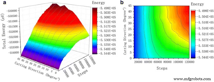
SiC 연마 충격 절단 공정을 위한 에너지 분석
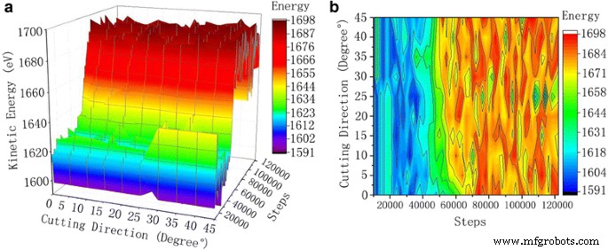
열역학 총 에너지는 시스템의 총 위치 에너지와 총 운동 에너지의 합으로, 연마 입자가 공작물에 수행한 작업의 영향을 나타냅니다. 시스템의 에너지 변화에 대한 탄화규소 연마재에 대한 절단 각도의 영향은 그림 7에 나와 있습니다. 단결정 구리 공작물 재료를 탄화규소 연마 입자로 절단하는 과정에서 연마 입자가 공작물 재료에 수행한 작업이 작용합니다. 두 가지 방법으로; 한 부분은 단결정 구리 원자의 열을 증가시키는 운동 에너지로 변환되어 연마 기능을 하는 탄화규소 입자와 접촉하고, 다른 부분은 단결정 구리 공작물의 내부 구조, 격자 변형 및 격자 변형의 변화를 허용하는 위치 에너지로 변환됩니다. 격자 에너지 방출.
<그림>
공작물 원자의 운동 에너지 곡선. 그림 7은 절단 과정에서 다양한 절단 각도의 운동 에너지 곡선입니다. 시뮬레이션 단계 수가 증가함에 따라 원자의 운동 에너지는 낮은 범위에서 변동하다가 변동 내에서 높은 범위로 변동합니다. 아 3D 곡선. ㄴ 윤곽
단결정 구리 공작물의 연마 입자 절단 과정에서 시스템의 운동 에너지는 SiC 연마재가 공작물 재료에 수행한 작업과 밀접한 관련이 있습니다. 매 순간 시스템에서 입자의 속도를 계산하여 전체 시스템 운동 에너지를 계산할 수 있습니다.
공식에서 \( {v}_{\mathrm{ix}}^2 \), \( {v}_{\mathrm{iy}}^2 \) 및 \( {v}_{\mathrm {iz}}^2 \)는 속도 성분 x를 나타냅니다. , y , z 방향 원자, 각각.
그림 7의 운동 곡선은 시뮬레이션 단계가 증가할 때 원자의 운동 에너지가 처음에는 낮은 범위에서 변동하다가 이후에는 높은 범위로 변동한다는 결론을 도출했습니다. 연마 입자의 이동과 함께 가장 바깥쪽의 구리 원자와 Si, C 원자(SiC) 사이에 장거리 반발 상호 작용이 발견됩니다. 공작물의 구리 원자는 운동 에너지를 얻고 움직이기 시작합니다. 탄화규소 입자가 구리 단결정과 접촉하면 접촉 영역의 원자 온도가 상승하여 원자 열 운동이 증가합니다. 절단이 안정적일 때 재료에 있는 구리 원자의 운동 에너지는 동적 평형 패턴으로 전달 및 변형되며 원자의 운동 에너지는 높은 범위에서 변동합니다.
운동 에너지 분석을 통해 절단 과정에서 입자가 공작물과 접촉하기 시작할 때 압출 영역의 원자가 격자 변형을 겪고 원자 좌표가 변경되며 운동 에너지에 따라 변위가 변경된다는 결론을 내렸습니다. 연마 입자가 단결정 구리에 들어가면 공작물이 공작물에 완전히 들어갈 때 단결정 구리 공작물의 운동 에너지의 피크 값이 나타납니다. 연마 입자의 운동 에너지와 위치 에너지는 단순히 상호 변환되기 때문입니다. 그러나 전체 시스템의 에너지는 공작물에 들어가는 움직이는 입자를 제외하고 변경되지 않습니다. 또한 탄화규소 입자의 움직임으로 인해 공작물 원자가 동시에 이동합니다. 원자 마찰 시 발생하는 열은 운동 에너지에 의해 방출되고 전위 운동으로 인한 변형 에너지 방출입니다.
공식에서 n 원자의 수입니다. vi는 순간 속도를 나타냅니다. ㅋ나 는 볼츠만 상수이고 T나 원자의 온도입니다.
절삭력은 연마제가 공작물 재료와 접촉하는 영역의 원자 온도를 증가시킵니다. 원자의 열 운동과 원자의 운동 에너지를 고려하면 구리 원자의 운동 에너지가 부분적으로 증가합니다. 시뮬레이션된 시스템은 표준 앙상블로 설정됩니다. 전체 시스템 온도는 특정 범위에서 변동합니다. 연마입자를 절단할 때 발생하는 열은 항온 원자층으로 빠르게 전달되기 때문에 시스템 전체의 운동에너지는 거의 변하지 않습니다.
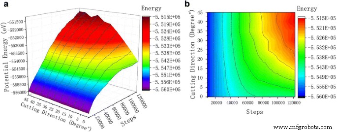
Fig. 8의 포텐셜 에너지 곡선에서 알 수 있듯이 시뮬레이션 단계가 증가할수록 공작물에 있는 구리 원자 단결정 사이의 포텐셜 에너지도 증가하는 경향이 있다. 탄화규소 연마제가 구리 공작물의 단결정과 접촉하면 처음부터 완전히 안정된 절단이 시작되고 공작물 재료가 점차 변형되고 구리 원자가 변위되어 결정의 결정 격자가 왜곡됩니다. 이것은 또한 변형 에너지가 증가하는 탄성 응력 필드를 생성합니다. 변형 에너지가 재료 원자를 재배열하기에 충분하지 않으면 원자의 전위가 발생하여 시스템의 총 에너지가 증가합니다. 0°에서 45°까지의 전위 곡선과 대조적으로 일정한 온도에서 원자의 열 운동의 일관성을 볼 수 있습니다. 원자 운동 에너지와 SiC 연마 입자의 절단 각도 사이에는 중요한 관계가 없습니다. 원자의 운동 에너지는 원자의 열 운동과 밀접한 관련이 있습니다. 그러나 위치 에너지와 총 에너지의 변화는 분명히 SiC 연마 입자의 절단 각도와 관련이 있습니다. 원자 위치 에너지의 크기는 절단 각도가 증가함에 따라 증가합니다. 절단 각도가 0°와 20° 사이일 때 위치 에너지의 명백한 변화가 관찰됩니다. 그러나 절단 각도가 25°와 45° 사이일 때 위치 에너지는 그대로 유지되며 전체 위치 에너지 곡선은 절단 각도 0°에서 20°입니다. 그림 9에서 보는 바와 같이 전체 에너지 경향은 위치 에너지 곡선의 경향과 유사하다. 모든 절단 각도의 총 에너지 값은 서로 매우 가깝습니다. 전체 에너지는 시스템의 위치 에너지 및 운동 에너지와 같지만 절단 과정에서 운동 에너지는 절단 각도에 따라 변하지 않기 때문입니다. 가공물의 운동 에너지 변화는 절단 각도에 따라 매우 낮습니다. 따라서 위치 에너지의 변화 곡선은 총 에너지 곡선과 유사합니다. 그림 9의 원자 변위 다이어그램을 비교하면 동일한 절삭 조건에서 단결정 구리 공작물의 절삭 깊이는 절삭 각도가 25°와 45° 사이일 때 더 커짐을 알 수 있으며, 이는 변위 증가에 기인할 수 있습니다. 구리 원자의. SiC 입자의 방향을 따라 격자 및 전위에서 더 많은 원자 손상이 발생합니다. 이 시간 동안 생성된 변형 에너지가 더 높기 때문에 높은 위치 에너지 변화 곡선과 공작물 원자의 총 에너지 변화 곡선이 발생합니다.
<그림>
공작물의 위치 에너지 곡선. 그림 8은 절단 과정에서 다른 절단 각도에서 위치 에너지 변화의 그래프입니다. 시뮬레이션의 단계 수가 증가함에 따라 단결정 구리 원자 전시 워크피스 사이의 전위가 증가하는 경향이 있습니다. 아 3D 곡선. ㄴ 윤곽
<그림>
총 에너지 곡선. 그림 9는 총 에너지 곡선을 보여줍니다. SiC가 단결정 구리 공작물을 절단하는 과정에서 공작물에 대한 연마 입자의 영향은 두 가지 형태로 나타납니다. 단결정 구리 공작물과 SIC 입자의 접합 영역; 다른 부분은 위치 에너지로 변환되고 단결정 구리 공작물의 내부 구조가 변경되고 격자가 변형되고 격자 에너지가 방출되어 위치 에너지로 변경됩니다. 아 3D 곡선. ㄴ 윤곽
SiC 연마 입자 충돌 절단 공정의 원자 변위 분석
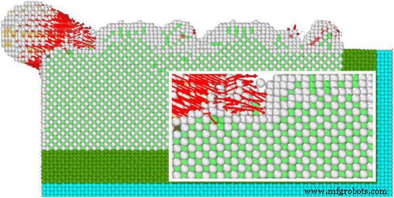
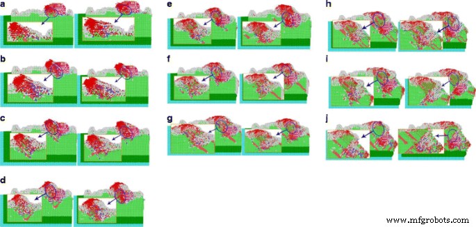
공작물 재료를 다양한 각도로 절단하는 과정에서 연마 입자는 절단 방향을 따라 이동하여 공작물의 구리 원자를 강제로 이동시킵니다. 공작물의 이동 방향 분석에서 연마 입자가 공작물 재료에 미치는 영향, 칩 형성 방식 및 재료 제거가 완전히 명확해집니다. Ackland-Jones가 제안한 결합각 분석 방법에 따르면 관찰 및 분석을 위해 서로 다른 원자 격자 구조가 다양한 색상으로 표시됩니다. ZOY 평면은 개별 SiC 입자의 절단 과정을 관찰하기 위해 선택되었으며 절단 영역의 원자 변위 다이어그램은 그림 10에서 볼 수 있듯이 확대됩니다.
<그림>
다른 절단 각도로 인해 원자 변위가 발생합니다. 그림 10은 다양한 절단 각도의 원자 변위를 설명합니다. 단결정 SiC 지립이 구리를 절단하는 공작물에 서로 다른 방향으로 충돌하여 SiC 지립이 절단되면 절단 방향의 속도가 80m/s, [001] 방향의 이동 속도이므로 절단 깊이가 증가합니다. v입니다 z =0.8 * sin θ , 절단 각도의 절단 깊이가 증가함에 따라 동일한 절단 각도에서 시뮬레이션 단계가 증가함과 동시에 절단 깊이가 큽니다. 아 0° 변위. ㄴ 5° 변위. ㄷ 10° 변위. d 15° 변위. 이 20° 변위. 에 25° 변위. 지 30° 변위. 아 35° 변위. 나 40° 변위. j 45° 변위. (원자색: HCP 구조, BCC 구조, 백색 비정질 구조로서의 FCC 구성)
단결정 SiC 연마 입자가 공작물과 충돌하여 구리를 다른 방향으로 절단하면 공정을 따라 절단 깊이가 증가합니다. 절단 방향의 속도는 80m/s이며, 여기서 [001] 방향의 구성요소 속도는 v입니다. z =0.8
*
죄 θ . At the same simulation step, cutting depth increases with increasing the cutting angle. As shown in Fig. 10, there is an atomic position shift in both of the surface and interior of the workpiece material, contacting with the abrasive grains, where atoms of different lattice types are arranged and doped with each other. Due to the movement of these abrasive particles, the copper atoms accumulated at the tip of the abrasive grains, which results no cracks during abrasive particles cutting. It can be seen that the material removal mode of the abrasive particles is plastic deformation. At the same time, due to abrasive cutting, the atoms displacement in single crystal copper increases from 15° to 45°.
The number of the workpiece atoms along the abrasive grain motion direction also increases, and the atomic displacement is perpendicular to the direction of abrasive cutting. This part of the atomic displacement is due to that of the abrasive particles, change the cutting action to the extrusion upon the workpiece atoms. At cutting angle, the abrasive particles is between 0° and 10°, while the cutting depth is smaller than those of the 15° to 45°. Abrasive particles are performing mainly the cutting function, the extrusion of the workpiece atoms is marginal, and the number of atoms is small whose displacement direction is perpendicular to the direction of the abrasive grain motion. With the repeated cutting on the workpiece surface by numerous abrasive particles, the abrasive particles having large cutting angle produce deep pits on the workpiece material during the whole cutting process, while ones following smaller cutting angles will continue cutting along the cutting mark produced by the former. Under the combined action, the workpiece material is cut to a certain depth (micro-cutting) followed by whole abrasive flow polishing.
Dislocation Collision Analysis for SiC Abrasive Cutting
Dislocation is a special arrangement of atoms in crystal along certain crystal surface and crystal direction, or a boundary between the slip zone and the non-slip zone on the slip surface. Dislocation can be divided into edge dislocation, spiral dislocation, and mixed dislocation, among which mixed dislocation is most common. In the process of abrasive particle cutting, the single crystal copper workpiece is plastically deformed, the atoms move, and the crystal lattice breaks and reconstructs, which results in a large number of dislocations. The analysis for dislocation and bond angles at different incidence angles is shown in Fig. 10. In the simulation model of abrasive flow simulation, two abrasive particles are used for cutting the workpiece material. For ease of analysis, the generation and change of different dislocation lines in single crystal copper material, during cutting process and the different lattice structures in the cutting part are analyzed in the view of one single SiC particle on the YOZ surface, as shown in Fig. 11.
Different angles-bond angle dislocation line charts. Figure 11 represents the cutting dislocation line and the bond angle. As the repeated cuttings on the workpiece surface are done by the numerous abrasive particles during the polishing process, in the entire cutting process, the abrasive particles with larger cutting angle produce bigger pits, while the following abrasive particles with smaller cutting angles continue to polish along the cutting trace. Therefore, certain depth is done on the workpiece material and the whole micro-cutting of abrasive flow polishing is achieved. 아 Dislocation lines with 0° cutting angles. ㄴ Dislocation lines with 5° cutting angles. ㄷ Dislocation lines with 10° cutting angles. d Dislocation lines with 15° cutting angles. 이 Dislocation lines with 20° cutting angles. 에 Dislocation lines with 25° cutting angles. 지 Dislocation lines with 30° cutting angles. 아 Dislocation lines with 35° cutting angles. 나 Dislocation lines with 40° cutting angles. j Dislocation lines with 45° cutting angles. (Note:the upper part of the key angle analysis, the figure in the atomic color: HCP BCC Amorphous structure Abrasive grain; the lower part of the dislocation line diagram, the figure dislocation line color: Stair-rod, Shockley, Hirth, Perect, Frank, Burgers vectors)
Key angle analysis diagram of each cutting angle is shown in Fig. 11, where the sample from the interior workpiece simulation at time 60 and 70 ps, the atoms are colored individually according to different arrangement of atoms through BAD technology. To facilitate the analysis of the lattice changes in the cutting part, atoms of the FCC structure in the workpiece material are removed. By DXA techniques, different types of dislocations are marked in diverse colors:red arrow indicates the Burgers vector (Burgers vectors), green for Shockley partial dislocations (Shockley), light blue for the Frank partial dislocations (Frank), pink pole position for the pressure error (Stair-rod), and blue for the whole dislocation (Perfect).
As can be observed from the analysis of the bond angle portion in Fig. 11, a large number of dislocations and lattice deformations occurred under the impact of external cutting forces. The bond angle analysis shows that the internal HCP structure of the workpiece appears more clearly with increasing of cutting angle. On further simulations, the structure of HCP increases gradually. The silicon carbide particles continuously cut and squeeze the workpiece material at 80 m/s speed, resulting in a phase transition from the FCC structure to the HCP structure. During this phase transition, the atomic strain of the workpiece continues to increase. However, when the stress state of atoms of the workpiece has exceeded the threshold of thermodynamic phase transition, it turns to metastable state. As the strain increases, the HCP phase begins to nucleate and grow spontaneously, and the FCC lattice of copper undergoes absolute destabilization, which induces a sudden change in mechanical quantities. As the kinetic energy of the atom is directly related to the atomic temperature (formula 1), there is a saltatory augment in the kinetic energy change curve, as can be seen from Fig. 7. This is due to high strain energy, accumulated in the single crystal copper workpiece before the nucleation of HCP. The HCP structure increases the system temperature through metastable nucleation and partial stress release. Due to the abrasive cutting and extrusion, bonds of copper atoms in workpiece material break down which results in disorder. The original regular lattice structure is broken, where the partial copper atoms gradually change into disorder and form an amorphous structure. It can be seen from the bond angle analysis diagram that (Fig. 11) atoms with relatively disordered displacement tend to form amorphous structures at 60 and 70 ps, which is because of silicon carbide abrasive particles. At the same time, many atoms with the same displacement direction are transformed into HCP structures. Meanwhile, the particles shear downward and the atomic structure is rearranged due to the displacement of atoms in the original amorphous structure, results an amorphous structure of HCP. Atoms that have already been transformed into HCP structures, even before the next cut stage, change back into amorphous structure. As the cutting depth increases, the number of amorphous atoms near the abrasive particles also increases.
When the FCC crystal structure undergoes cutting by abrasive particles, a shear stress generates in atoms, which results in the displacement of atoms in the lattice and the arrangement of various lattice structures. In moving the atoms of workpiece, the rigid displacements of the atoms produce dislocations, also called as dislocation lines (Fig. 11). Dislocation line can be termed as the boundary between the slip zone and the non-slip zone, on the slip surface. According to the relation between the dislocation and the PATS vector, dislocation is parallel to the PATS vector, called the screw dislocations. The vertical ones are edge dislocations, and the mixed dislocations are neither parallel nor vertical. In Fig. 11, most of the dislocation lines are neither parallel nor vertical to PATS vectors, which are typical mixed dislocations. In the cutting process of abrasive particles, the dislocation line changes, moves and grows around the abrasive particles. The closer the particle, the greater the density of the dislocation line. Dislocation lines are also very dense, when the arrangement of atoms is complicated. The abrasive particles marked as orange, produce a large amount of HCP, BCC, and amorphous structures around them, which interlace and blend with each other to form dislocations that increases the internal energy of the crystals. When atoms arrange their self just like shown in Fig. 12b, possess maximum potential energy. While for the arrangement, shown in Fig. 12a–b, the atoms situate at the lowest potential energy position. The number of dislocation lines is directly related to the magnitude of strain energy of the crystal. The total strain energy of the unit length dislocation can be measured with the given formula:
$$ W=\alpha {Gb}^2 $$ (3)
Schematic view of dislocation changes. Dislocation is a special arrangement of atoms in crystals. It is the crystal in the atomic arrangement along a certain crystal face and crystal orientation occurred in a certain wrong line, and it is the boundary of the slip surface within the area where the slip has occurred and the area with no slip has occurred. In Fig. 12a –ㄷ , the relative displacement of the rigidity of the upper atom and the underlying atom produce dislocations, the upper atom belongs to the sliding region, and the lower atoms belong to the non-slip region, they are in the slip surface of the intersection line which is called dislocation line, that is, dislocation. Figure 12 is the process of dislocation generation and development
Where, α is the geometric factor (type dislocations, dislocation density) parameter related to, and generally 0.5 ~ 1.0; G is the shear modulus, and b is the slippage distance.
When the workpiece material is being cut, particles break the atomic arrangement and the lattice reconstructs, which constitutes, macroscopically, the plastic deformation of the workpiece material. In the process of plastic deformation, the dislocation was supposed to escape from the crystal and decrease the dislocation density. However, this dislocation density increases due to dislocation propagation. There are many ways of dislocation multiplication and the main one is the Frank–Reed dislocation source theory, of which the growth mechanism is shown in Fig. 11. As illustrated in Fig. 11, the density of the dislocation line increases markedly from 60 to 70 ps when the cutting simulation proceeds, change both the number and shape of dislocation lines in accordance with Frank–Reed dislocation source theory. At simulation time of 60 ps, there are many long Shockley dislocations. But after another 10 ps simulating, the long Shockley dislocation line becomes less and shorter. The original straight dislocation lines turn into bent, which is especially evident near the abrasive grains. From formula 3, the strain energy of the dislocation is proportional to b
2
. From the viewpoint of energy, the dislocations with the smallest b in the crystal should be most stable with low energy; however, dislocations with larger b will break down into ones. In addition, the energy of the dislocation is valued by the unit length of the dislocation line. Given the shortest line between two points is the straight, the strain energy of straight dislocation is lower than that of the bent one, means straight dislocations are more stable. Frank–Reed dislocation source theory argued that the long dislocation line becomes shorter and breaks down into smaller dislocations, thus decreasing the strain energy of the crystal.
Analysis for Friction Coefficient Between Workpiece Surface and Abrasive Particles
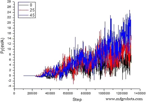
To quantitatively disclose mechanical properties and surface effect of SiC abrasive cutting single crystal copper material, the tangential force ([010] direction) and normal force ([001]direction) on the cutting surface are further analyzed. The friction coefficient can be defined as the ratio of the tangential force to the normal force, with the formula below:
$$ f=\frac{F_y}{F_z} $$ (4)
Figure 13 shows the variation of friction coefficient along different cutting angles during abrasive cutting. The change of friction coefficient can be divided into two periods. Period I, when the cutting distance is less than half of the size of the abrasive particle, the friction coefficient fluctuates violently in certain range due to surface effect of the material; while in period II, all the friction coefficients fluctuate in very small range, and the friction coefficients remains steady state at different angles. However, at cutting angle of 5°, there is a small amount of abnormal fluctuation at the end of simulation. Moreover, in period I, abrasive particles contact the workpiece atoms to the abrasive grains enter into the workpiece of half abrasive diameter (shown in Fig. 13b), the cutting movement distance reaches 7.5 Å. In Fig. 6, the cutting force change curve shows that the tangential force and normal force are in an oscillating phase during period I. Since the friction coefficient can be characterized as the adhesion among atoms in the contact surface and is related to the two atoms contacting with each other, regardless of the cutting mode, which can interpret the phenomenon that change of cutting angle does not cause significant change of friction coefficient, as shown in Fig. 13a.
Friction coefficients of different cutting angles. Figure 13 is the changes of the frictional coefficients during SIC particles cutting single crystal copper from different angles. The change in cutting angle did not cause significant changes in friction coefficient. It described two kinds of coefficient of friction in contact with the relevant atoms in the cutting process, regardless of the cutting mode. 아 Friction coefficient variation curve with cutting angle. ㄴ Instantaneous structure when SiC abrasive grains move 7.5 Å
결론
The micro cutting simulation of single crystal copper by SiC abrasive particles is achieved during abrasive flow polishing. Comprehensive analysis of the SiC abrasive cutting reveals that when SiC abrasive particles cut at angle from 0° to 15°, cutting forces in along Y and Z direction are relatively small and tend to stay steady. A larger cutting angle results more dislocations, which brings about larger grooves damaging of the workpiece material. In the process of cutting, it is necessary to avoid more dislocations, which has an immediate adverse effect on the performance of all aspects of crystal material. Therefore, a cutting angle of 0° is better than other angles. Considering the amount of dislocation produced, or the change of cutting force and energy in the cutting process; cutting with small or medium angles is not only beneficial for improving surface quality but reduce the internal defects.


 HCP 구조,
  BCC 구조,
  백색 비정질 구조로서의 FCC 구성)
 HCP
HCP  BCC
BCC  Amorphous structure
  Abrasive grain; the lower part of the dislocation line diagram, the figure dislocation line color:
 Stair-rod,
  Shockley,
  Hirth,
  Perect,
  Frank,
  Burgers vectors)
