

나노물질

산업 제조
우리는 이론적으로 하전 와이어로 모델링된 두 개의 병렬 게이트 사이의 나노나선에 전자가 국한되어 있는 문제를 조사합니다. 이중 게이트 나노 나선 시스템은 게이트 전압에 매우 민감한 특성을 가진 이진 초격자입니다. 특히, 밴드 구조는 게이트 전압의 특정 조합에 대해 에너지 밴드 교차를 나타내며, 이는 준상대론적 Dirac과 유사한 현상으로 이어질 수 있습니다. 선형 및 원형 편광에 의해 유도된 광학 전이에 대한 우리의 분석은 이중 게이트 나노나선이 다양한 광전자 응용 분야에 사용될 수 있음을 시사합니다.
첫 번째 저자가 어린 시절 열정적으로 수집한 화석화된 나선형 복족류부터 선사 시대 생물을 정의한 DNA의 얽힌 구조에 이르기까지 나선 기하학은 자연 전체에 널리 퍼져 있습니다[1]. 자연적으로 발생하는 생체 분자의 모양에 기인한 복잡한 기능에서 영감을 받아[2-6], 나노 기술에 적합한 나선형 기하학을 가진 다른 시스템이 풍부한 물리학을 산출하고 새로운 응용에 기여할 것으로 예상됩니다. 지난 30년 동안 나노 제조 기술의 눈부신 발전으로 InGaAs/GaAs[7], Si/SiGe[8], ZnO[9–11], CdS[ 12], SiO2 /SiC[13, 14], 순수 탄소[15–20], II-VI 및 III-V 반도체[21](최신 기술 상태는 참고문헌[21–26] 참조). 결과적으로, 토폴로지 양자화된 전하 펌핑[27, 28], 초전도성[29], 스핀 필터링[30-32]과 같은 이국적인 수송 특성에서 분자 및 나노기계적 신축성 전자장치[33, 34] 압전 효과[35], 센싱 응용[36, 37], 에너지[38] 및 수소 저장[39], 전계 효과 트랜지스터[40, 41]로 인한 것입니다.
나노 나선 기반 장치의 매력은 궁극적으로 나선 구조의 토폴로지에 인코딩된 고유한 주기성에서 비롯됩니다. 특히, 나노나선에 가로 전기장(나선 축에 수직)을 가하면 초주기 전위에서 전자의 브래그 산란과 같은 초격자 거동이 발생하여 초격자 브릴루앙 영역의 가장자리에서 에너지 분할이 발생합니다. 전기장에 의해 선형으로 조정 가능한 가장 낮은 상태[42, 43]. 이 거동은 Bloch 진동과 음의 차동 전도도를 유발할 수 있으며[44, 45], 나선을 통한 스핀 편극 수송을 강조할 수 있을 뿐만 아니라[31, 46], 나노광자 카이로광학 응용에 유용한 원형 이색성 향상을 생성할 수 있습니다[47]. 이 시스템은 단항 초격자(unary superlattice)를 구성하고, 테라헤르츠 범위에서 주파수 증폭, 증폭, 복사 생성 또는 흡수를 위한 터널 다이오드 또는 건 다이오드로 나노나선을 사용할 가능성을 더욱 열어줍니다[48-51]. 원형 초격자는 일반적으로 서로 다른 고유 밴드 갭을 갖는 교대 반도체 층의 이종 구조에서 실현되지만 나노나선 초격자의 매개변수는 외부 필드에 의해 완전히 제어됩니다. 반대로, 기존의 기존 초격자 전위의 모양은 이종 구조에 고유하며 견고하지만 큰 외부 필드를 사용하지 않고 활용하는 과정에서 제한된 조작 능력을 제공합니다. 따라서 나노나선을 초격자로 사용하는 것의 매력은 더 큰 조정 가능성에 있습니다.
반면에 이종구조 반도체 초격자(또는 실제로 광자 초격자 구조[52-55]와 광학 격자의 차가운 원자[56, 57])를 사용하면 나선을 따라 전기장. 이진 초격자[58-60]로의 확장조차도(단위 셀이 두 개의 다른 양자 우물 및/또는 장벽으로 구분됨) Bloch-Zener 진동[61]과 같은 풍부한 물리학 배열을 약속하며, 이는 차례로 기여할 수 있습니다. 조정 가능한 빔 스플리터 및 간섭계 애플리케이션 [62]. 따라서 나노나선 기반 초격자의 외부 필드 조정 가능성과 이진 초격자의 우수한 기능을 결합하는 것이 매우 바람직합니다.
다음에서 우리는 나선 축과 정렬된 두 개의 평행 게이트 대전 와이어 사이에 나노 나선이 위치한 시스템을 설명합니다. 우리는 추가 가로 전기장의 적용을 예상하고 이론적으로 게이트 및 필드 제어 가능한 전위가 1차원 나선을 따라 이진 초격자를 구성한다는 것을 보여줍니다.
N이 있는 단일 전자 반도체 원형 나노 나선의 경우를 연구하여 시작하겠습니다. 반경 R 회전 , 피치 p , 총 길이 L =Np . 나노구조는 z를 따라 정렬된 나선 축과 함께 하전 와이어로 모델링된 두 개의 평행 게이트 사이에 위치합니다. -축 및 축 및 게이트가 모두 그림 1에 표시된 것처럼 동일한 평면에 있습니다. 또한 게이트 축 평면에 수직인 외부 횡전계를 고려합니다. \(\mathbf {E}=E_{\bot } \ 평면 아래 전위에 대한 평면 위 전위의 반사 대칭을 깨는 데 사용할 수 있는 모자 {\mathbf {y}}\). r을 통해 매개변수로 설명된 나선형 좌표에서 작업합니다. =(x,y ,z )=(R cos(s φ ),R 죄( φ ),ρ φ ), 여기서 동적 각도 좌표 φ =z /ρ ρ가 있는 나선 축을 따른 거리에만 의존 =피 /2π , 및 s =±1은 각각 왼쪽 또는 오른쪽 나선을 나타냅니다. 이 작업에서 우리는 왼손잡이 나선 s를 고려합니다. =1. 유효 질량 모델의 틀에서 에너지 스펙트럼 ε v v의 이러한 외부 전위의 영향을 받는 나선에서 전자의 고유 상태는 슈뢰딩거 방정식에서 찾을 수 있습니다.
$$ -\thinspace \frac{\hbar^{2}}{2M^{*}\rho^{2}}\frac{d^{2}}{d\varphi^{2}}\psi_{\ nu} +\left[V_{g} (\varphi) + V_{\bot} (\varphi) \right]\psi_{\nu} =\varepsilon_{\nu} \psi_{\nu} $$ (1 ) <그림>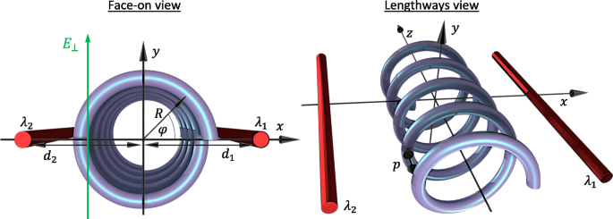
정면 및 세로 관점 모두에서 시스템의 지오메트리 및 매개변수 다이어그램. R 는 나선 반경이고 d 1 그리고 d 2 전하 밀도가 λ인 나선 축에서 대전된 와이어의 거리입니다. 1 및 λ 2 , 각각. 공간 좌표 φ 나선의 각도 위치를 정면에서 설명하고 z와 관련이 있습니다. - φ를 통한 좌표 =2π z /p p와 함께 나선의 피치. 가로 전기장 E ⊥ y -축
여기서 전자 유효 질량 M을 기하학적으로 재정규화했습니다. e M에게 * =엠 e (1+R 2 /ρ 2 ) 나선 축을 따라 좌표로 모든 것을 표현하기 위해 (φ =z /ρ ) 외부 전위에 대해 더 편리합니다. 자, V ⊥ (φ )=−eE ⊥ R 죄(φ )는 y를 따라 향하는 가로 전기장의 기여도입니다. -축과 같은 V ⊥ (π /2)<0. 게이트의 전위는 V입니다. g (φ )=−e [Φ 1 (φ )+Φ 2 (φ )] Φ로 주어진 개별 대전 와이어로 인해 나선을 따라 전자가 느끼는 정전기 전위 나 (φ )=−λ 나 ㅋ ln(r 나 /d 나 ). 여기, 나 =1,2는 전선에 레이블을 지정합니다. λ 나 는 와이어의 선형 전하 밀도이고 \(k =1/2\pi \tilde {\epsilon }\)이고 \(\tilde {\epsilon }\) 절대 유전율입니다. 특정 와이어에서 테스트 전하의 수직 거리는 \(r_{i}=[d^{2}_{i}+R^{2} + 2(-1)^{i}d_{i }R\cos (\varphi)]^{1/2}\), d 포함 나 나선의 축에 대한 와이어의 해당 거리를 나타냅니다. 우리는 나선의 축을 따라 제로 게이트 유도 전위를 정의했습니다. 전체 1차원 전위 V T (φ )=V g (φ )+V ⊥ (φ ) 분명히 주기적 V T (φ )=V T (φ +2π n ) 마침표 2π 일반적으로(p 기간에 해당 좌표 z를 기준으로 ). 이 기간은 원자간 거리보다 훨씬 더 크며 전형적인 초격자 효과를 일으킵니다. 이 문자는 가로 전기장의 나노나선과 다릅니다(V로 재현할 수 있음). T (φ )=V ⊥ (φ ) 여기에서) 주로 이중 게이트 전위 V를 통해 초격자의 반복 단위 셀을 조작함으로써 g (φ ). 제한 p →0, 두 개의 정전기 게이트가 있는 고리 그림의 입자로 돌아갑니다[63, 64]. 근사값 R 만들기 /d 나 ≪1, V를 확장할 수 있습니다. g (φ ) cos(φ에서 2차까지) ), 식을 변환할 때 1 무차원 형태로
$$ {\begin{정렬} \frac{d^{2} \psi_{\nu}}{d\varphi^{2}}+\left[\epsilon_{\nu} + 2A_{g}\cos( \varphi) + 2B_{g}\cos(2\varphi) + 2C_{\bot} \sin(\varphi) \right]\psi_{\nu} =0, \end{정렬}} $$ (2)에너지 규모 \(\varepsilon _{0}(\rho) =\hbar ^{2} / 2 M^{*} \rho ^{2}\) 단위의 양은
로 정의됩니다. $$\begin{array}{@{}rcl@{}} A_{g} &=&\beta\frac{\left(d_{1}^{2} +R^{2}\right)}{ d_{1} R}(1-\감마), \qquad B_{g} =\frac{\beta}{2}\left(1+\frac{\lambda_{1}}{\lambda_{2}} \gamma^{2}\right), \\ C_{\bot} &=&e E_{\bot} R /2\varepsilon_{0}(\rho), \qquad \qquad \qquad \; \epsilon_{\nu} =\frac{\varepsilon_{\nu}}{\varepsilon_{0}(\rho)}. \end{배열} $$ (3)여기서 \(\beta =ek d_{1}^{2} R^{2} \lambda _{1} /2\left (d_{1}^{2} +R^{2}\right)^ {2}\varepsilon _{0}(\rho) \)는 게이트 1의 기여를 특성화하는 반면 비대칭 매개변수 \(\gamma =\lambda _{2} d_{2} \left (d_{1}^{2 } +R^{2}\right)/\lambda _{1} d_{1} \left (d_{2}^{2} + R^{2}\right)\)는 게이트 2의 상대적 기여도를 나타냅니다. , γ 포함 =1 전위에 대한 동일한 게이트 기여에 해당(결과는 A) g =0). d 유지의 어려움으로 인한 불가피한 비대칭에 유의해야 합니다. 1 =d 2 λ를 조작하여 보상할 수 있습니다. 1 및 λ 2 . 이 편지에서 우리는 γ를 고려하도록 제한합니다. ≤1(이는 |Φ 1 |>|Φ 2 |) 1보다 큰 비대칭 매개변수는 게이트에 레이블을 지정하는 인덱스의 간단한 교환과 관점 φ의 해당 이동을 통해 1보다 낮은 동등한 시스템에 매핑될 수 있습니다. →φ ±π . 또한 C ⊥ 음의 C 대칭으로 인해 ≥0 ⊥ φ의 좌표 변환과 관련하여 , 및 A g ≥0, B g >0(즉, 와이어 β의 양전하 밀도만)>0) 음으로 대전된 게이트가 있는 모든 잠재적인 풍경은 양으로 대전된 게이트의 매개변수의 올바른 조합으로 재현될 수 있습니다. 그림 2에서 무차원 전위 V를 플로팅합니다. T (φ )/ε 0 (ρ ), π의 강도로 - B에 고정된 주기적인 잠재적 구성요소 g =0.2, 2배 주기 섭동 매개변수 A의 여러 조합에 대해 g 및 C ⊥ . 우리는 총 외부 전위가 φ를 따라 이진 초격자를 유도한다는 것을 알 수 있습니다. , 파란색으로 강조 표시된 단위 셀로 이중 양자 우물(DQW)이 있습니다. 이것은 상대적인 게이트 기여도 γ를 조작하여 질적으로 다른 형태를 취할 수 있습니다. 및 횡전계 E ⊥ . 단위 셀은 본질적으로 동등한 게이트 기여(γ =1) 가로 전기장 없음 E ⊥ =0(A에 대한 그림 2a에서와 같이 g =C ⊥ =0). E 수정 ⊥ =0, 더 강력한 게이트 1 기여도(γ <1), 단위 셀은 웰 최소값과 퇴화 장벽 최대값이 다른 DQW가 됩니다(그림 2b에서 A g =0.1 및 C ⊥ =0). 대조적으로, DQW 최소값을 퇴화 상태로 유지하고 서로에 대해 두 개의 잠재적 장벽을 조작하려면 대칭 게이트 기여(γ =1) 0이 아닌 전기장에서 E ⊥ ≠0(A가 있는 그림 2c g =0 및 C ⊥ =0.1). 비대칭 게이트 기여 결합(γ <1) E ⊥ ≠0은 잠재적인 유정 최소값과 장벽이 다른 DQW를 생성합니다(그림 2d에서 볼 수 있듯이 A g =C ⊥ =0.1). 이는 다음 섹션에서 볼 수 있듯이 질적으로 다르고 풍부한 행동으로 이어집니다.
<그림>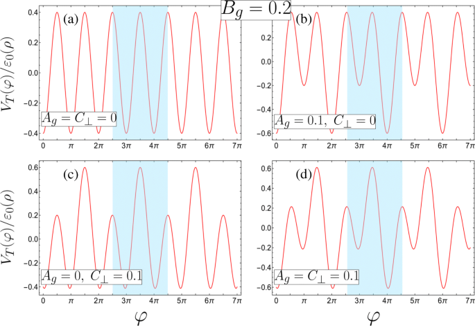
파란색으로 강조 표시된 단위 셀이 있는 4가지 가능한 초격자 전위 구성(무차원 매개변수로 정의됨, 물리적 매개변수의 해당 요구사항은 식 3 참조, 모두 B g =0.2). 아 단위 셀(A g =C ⊥ =0). ㄴ –d b 중 하나에서 형성된 이진 초격자 최대 축퇴로 인한 최소값 및 내부 반사 대칭이 다른 비대칭 DQW(A g =0.1, C ⊥ =0), c 축퇴 최소값만 있는 대칭 DQW(A g =0, C ⊥ =0.1) 또는 d 최소값과 최대값이 다른 비대칭 DQW(A g =C ⊥ =0.1)
식에 대한 솔루션 2는 Bloch 함수의 관점에서 찾을 수 있습니다.
$$ \psi_{n,q}(\varphi)=(2\pi N \rho)^{-\frac{1}{2}}e^{iq \varphi}\sum_{m} c^{( n)}_{m,q} e^{im \varphi}, $$ (4)여기서 q =카 z ρ 전자 준운동량 k의 무차원 형태 z 나선의 축을 따라 n 서브밴드를 나타내며, 전인자는 φ의 관점에서 정규화에서 발생합니다. :\(\rho \int _{0}^{2\pi N}|\psi _{n,q}(\varphi)|^{2} d\varphi =1\). 결과 표현식에 \(e^{im^{\prime } \varphi }/2\pi \)를 곱하고 φ에 대해 적분하여 지수 함수의 직교성을 활용합니다. , 여기서 m ′ 계수 \(c^{(n)}_{m,q}\),
에 대한 무한 연립 방정식 세트에 도달하는 정수입니다. $$ {\begin{정렬} &\left[(q+m)^{2}-\epsilon_{n}\right]c^{(n)}_{m} - \left(A_{g} - i C_{\bot} \right)c^{(n)}_{m-1} - \left(A_{g} + i C_{\bot} \right)c^{(n)}_{m +1}\\ &\quad- B_{g}\left(c^{(n)}_{m+2}+c^{(n)}_{m-2} \right)=0, \ 끝{정렬}} $$ (5)명확성을 위해 q -아래 첨자 표기가 삭제되었습니다. ε n,q ≡ε n 및 \(c_{m}^{(n)}\equiv c_{m,q}^{(n)} \). 방정식 5는 시스템이 q에서 주기적임이 분명한 무한 오대각 행렬을 나타냅니다. , 그리고 − 1/2≤q로 정의된 첫 번째 Brillouin 영역으로 고려 사항을 제한할 수 있습니다. ≤1/2. 초격자 전위 A가 없는 경우 g =나 g =C ⊥ =0이면 고유값이 m으로 열거됩니다. ε로 주어진 m =(m +q ) 2 그리고 우리는 m을(를) 인식합니다 나선의 자유 전자와 관련된 각운동량 양자수입니다. 우리는 식에서 봅니다. 5 A일 때 g =C ⊥ =0 Δ가 있는 상태만 나 =±2가 혼합되는 반면, A를 통해 달성되는 웰 최소값 또는 장벽이 다른 DQW 단위 셀의 형성 g ≠0 및/또는 C ⊥ ≠0, 상태도 Δ와 혼합 나 =± 1. 흥미롭게도, 외부 횡전위(나선의 1회전에 걸쳐 변함) 하에서 나선상의 전자 시스템은 수학적으로 자기장에 의해 관통되고 각도 좌표를 따라 변화하는 동일한 기능적 형태; 예를 들어 참조 참조. [65-67] 또는 예를 들어 Refs. [42–45]와 [68–70]. 반지의 경우 q가 수행하는 역할 여기에서 자속이 차지합니다. 따라서 이 작업에서 정확히 동일한 분석이 이중 게이트 양자 링[63-66]의 문제에 적용할 수 있으며, 링이 자속에 의해 관통되어야 합니다.
Eq.에 해당하는 행렬을 자르고 수치적으로 대각화합니다. 5는 n을 제공합니다. th 부대역 고유 에너지 ε n q의 각 값에 대한 계수 \(c_{m}^{(n)}\) . |m에서 잘림을 적용합니다. |=10, 매트릭스 크기의 증가가 가장 낮은 부대역에서 눈에 띄는 변화를 일으키지 않는다는 사실을 알고 있기 때문에 안전합니다.
여러 매개변수 조합에 대해 가장 낮은 대역의 에너지 분산을 그림 3에 표시합니다. 초격자의 형태에 따라 분산 거동의 현저한 다양성을 발견하고 매개변수의 일부 특정 조합에 대해 Brillouin 영역의 가장자리(그림 3a 및 c) 또는 Brillouin 지역의 중심(그림 3b 및 d).
<그림>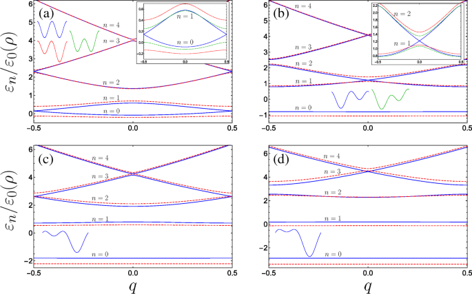
무차원 매개변수의 다양한 조합을 위한 이중 게이트 나노 나선 시스템의 밴드 구조(B 포함) g =0.4 전체 고정):a 파란색 실선(빨간색 점선) 플롯 A g =0 &C ⊥ =0(A g =0.2 &C ⊥ =0), 삽입은 A를 사용하여 가로 전기장에 영향을 받는 하위 2개 부대역의 동작을 추가로 플롯합니다. g =0 &C ⊥ =0.2는 점선 녹색 곡선입니다. ㄴ 파란색 실선(빨간색 점선) 플롯 A g =0.63 &C ⊥ =0(A g =0.8 &C ⊥ =0) 파란색 곡선이 Brillouin 구역의 중심에서 교차하는 에너지 밴드와 함께 공명의 첫 번째 사건(텍스트 참조)을 묘사하는 곳에서 삽입된 그림은 A g =0.63 &C ⊥ =0.2는 점선 녹색 곡선입니다. ㄷ 파란색 실선(빨간색 점선) 플롯 A g =1.26 &C ⊥ =0(A g =1.5 &C ⊥ =0) 여기서 파란색 곡선은 더 높은 밴드에 대한 Brillouin의 가장자리에서 닫히는 에너지 갭과 공명의 두 번째 입사를 나타냅니다. d 세 번째 공명과 더 높은 서브밴드 미니갭은 중앙에서 닫히고 파란색 실선(빨간색 점선)은 A입니다. g =1.9 &C ⊥ =0(A g =2.2 &C ⊥ =0). 단위 셀 모양이 스케치됩니다. n 밴드를 열거하고 삽입 축은 기본 그래프와 동일합니다.
A일 때 g =C ⊥ =0일 때 단위 셀은 두 개의 등가 양자 우물을 구성하고 결과적으로 Brillouin 영역 가장자리에서 접하는 밴드 쌍의 모양이 자연스럽게 발생합니다. 실제로 하나의 우물을 단위 셀로 사용하면 초격자 기간이 절반으로 줄어들고 결과적으로 브릴루앙 영역이 두 배가 됩니다. 1≤q ≤1. 그런 다음 q에서 접지와 첫 번째 밴드 사이의 밴드 갭이 있는 일반적인 단항 초격자 밴드 다이어그램을 관찰합니다. =1은 n 사이의 밴드 갭을 통해 제공됩니다. =1 및 n q에서 =2 =0이고 B에서 선형입니다. g 교란 이론에서. 그래도 |q에서 밴드 구조에 대한 설명을 제공합니다. |=부록의 행렬 대수학을 사용하는 DQW 단위 셀 그림의 1/2입니다. 그림 3a의 삽입에서 볼 수 있듯이 이중 주기 전위 항 중 하나의 도입은 Brillouin 영역 가장자리에서 밴드 갭을 엽니다. 대칭 게이트 기여의 단위 셀(A g =0) 가로 필드 C의 적용 하에 대칭 DQW의 형태를 유지합니다. ⊥ 하나의 전위 장벽이 다른 하나에 대해 수정된 헬릭스 게이트 축에 수직입니다(그림 3a의 녹색 DQW 스케치로 표시). 동안 C ⊥ 밴드 갭이 열리면 분산 수정은 적용된 A와 유사한 크기의 분산 수정보다 현저히 덜 민감합니다. g . 이것은 |q의 더 작은 밴드 갭에서 볼 수 있습니다. |=1/2(A 포함) 그림 3a의 삽입에서 녹색 점선 g =0 및 C ⊥ =0.2) 빨간색 점선 곡선의 더 큰 간격(A용)과 비교 g =0.2 및 C ⊥ =0). 이 거동을 강조하기 위해 그림 4a는 |q에서 에너지 갭 크기를 표시합니다. |=고정 B<의 경우 두 개의 가장 낮은 부대역 사이의 1/2 \(\Delta \varepsilon _{01}^{(q=1/2)}/\varepsilon _{0}(\rho)\) /나> g =0.25 C 둘 다의 함수 ⊥ (A와 함께 g =0) 및 A g (C와 함께 ⊥ =0), 각각 녹색 점선 및 빨간색 점선 곡선입니다. 제로 횡전계 및 비대칭 게이트 전위(C ⊥ =0 및 A g ≠0), 단위 셀은 비대칭 DQW이지만 등가 장벽으로 인해 우물 최소값에 대한 내부 반사 대칭이 있습니다. 그러면 A 변화에 대한 밴드 갭의 더 높은 감도를 이해할 수 있습니다. g 초격자가 구성되는 격리된 DQW 단위 셀의 속성을 고려하여. A와 함께 g =C ⊥ =0, |q |=1/2(Brillouin 영역의 가장자리), 바닥에서 형성된 Bloch 상태와 격리된 DQW 단위 셀의 첫 번째 여기 상태(그림 4a의 파란색 회로도 및 수반되는 파동 함수 참조)는 임의 단계. 이 상황은 그림 3a의 갭리스 청색 분산 곡선에 해당합니다. 녹색 DQW 스케치를 통해 그림 4a에 개략적으로 도시된 바와 같이, C ⊥ DQW 최소값은 퇴화 상태로 유지되는 동안 다른 장벽에 대한 장벽 중 하나의 상대 최대값을 줄입니다. 따라서 격리된 DQW의 바닥 상태는 더 작은 전위 장벽에서 확률 분포의 약간의 증가에 의해서만 수정되며(교란되지 않은 바닥 상태에 비해 에너지가 약간만 감소함) 첫 번째 여기 상태는 본질적으로 변경되지 않은 상태로 유지됩니다. 노드가 장벽 아래에 위치하고 변동에 민감하지 않기 때문입니다. 이러한 바닥 및 첫 번째 여기 상태로 구성된 Brillouin 구역 가장자리의 Bloch 상태는 더 작은 장벽 아래에서 바닥 상태 파동 함수의 감소된 감쇠에서만 교란되지 않은 경우와 다릅니다(녹색 DQW와 파란색 DQW를 비교하십시오. 그림 4a). A 변경 g 장벽이 퇴화하는 동안 DQW 최소값의 상대적 위치를 조작합니다. 두 개의 가장 낮은 격리된 DQW 상태의 파동 함수는 상당히 다르며, 기저 상태는 단일 깊은 우물의 국부적 기저 상태를 향하는 경향이 있고 첫 번째 여기 상태는 더 얕은 유정의 국부적 기저 상태를 향하는 경향이 있습니다[71]. 섭동이 바닥 상태의 에너지를 낮추는 반면, A가 증가함에 따라 얕은 우물의 최소값이 위로 이동함에 따라 첫 번째 여기 상태의 에너지가 상대적으로 증가합니다. g , 결과적으로 A에 대한 밴드 갭 크기의 더 높은 감도 g . 특히, 지상 서브밴드의 입자는 A가 증가함에 따라 가장 깊은 포텐셜 우물의 바닥 근처에 빠르게 갇히게 됩니다. g . 따라서 가장 낮은 대역은 횡전계의 경우보다 더 빠르게 분산 없는 평면 대역에 접근하며, 이는 고밀도 상태를 수반하는 전자적 불안정성과 강력한 상호 작용 효과를 초래할 수 있습니다[72].
<그림>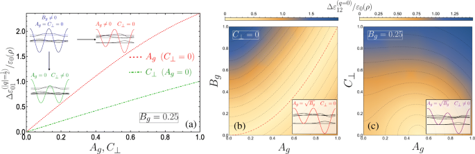
아 A의 함수로서 접지와 첫 번째 부대역 사이의 밴드 갭 크기 g (C ⊥ ) 빨간색 점선(녹색 점선)으로 표시됩니다(여기서는 B). g =0.25. 다이어그램은 격리된 DQW 단위 셀과 고유 상태에 대한 다양한 섭동의 영향을 나타냅니다. ㄴ –ㄷ 2D 밀도 플롯을 통해 표시되는 첫 번째 및 두 번째 부대역 사이의 밴드 갭 크기는 다음과 같은 함수로 표시됩니다. ㄴ A g 그리고 B g C용 ⊥ =0 및 c A g 및 C ⊥ 고정 B g =0.25. ㄴ 인접한 등에너지 등고선은 0.17의 차이를 나타내며 \(A_{g}=\sqrt {B_{g}}\)에 대해 점선 빨간색 선으로 주어진 간격이 0인 반면 c 차이는 0.13이며 가장 작은 반원 윤곽(0.5,0)의 중심에 간격이 없습니다. 다이어그램은 격리된 DQW 및 고유 상태를 스케치합니다. 혼성화는 s 사이에서 발생하지 않습니다. -좋아요 및 p - b에서 공명과 같은 국지화된 개별 우물 상태 , 하지만 c에서 수행 전기장이 다른 장벽에 대해 한 장벽을 변경하기 때문에
C를 유지하면 ⊥ =0 및 A 증가 g , 처음에는 모든 축퇴가 해제되지만 이후의 더 높은 에너지 밴드는 Brillouin 영역의 중심과 가장자리 사이를 번갈아 교차하도록 가져옵니다(그림 3a에서 d까지 진행되는 파란색과 빨간색 점선 곡선이 번갈아 나타나는 동작 관찰). 물리적으로 우리는 단위 셀에서 국부적인 파동 함수의 상호 작용 측면에서 소실 밴드 갭을 이해할 수 있습니다. 비대칭 DQW 전위가 얕은 우물의 바닥 상태(s -like 궤도)는 깊은 우물(p)에서 첫 번째 여기 상태와 공명합니다. -유사 궤도), q에서 =0 어느 쪽 우물의 중심에 대한 반사 대칭으로 인해 이러한 상태의 반대 패리티는 그들 사이의 일반적인 터널 커플링을 방지하고 결과적으로 이러한 궤도에서 구성된 여기 상태가 일치합니다(그림 3b의 파란색 곡선). 이것은 소위 s를 연상시킵니다. -피 광학 격자의 공명 [73, 74]. 같은 이유로, 매개변수가 얕은 우물의 국부적인 바닥 상태가 동일한 패리티를 갖는 깊은 우물의 여기 상태와 공진하는 것과 같으면 |q |=1/2일 때 Bloch 상의 존재는 두 인접 국부 우물 상태 사이의 일반적인 혼성화를 완전히 억제하고 밴드 갭이 닫힙니다(그림 3c에서 두 번째 여기 상태로 접지 공진에 대해 표시됨). 주기적 잠재력에서 산란의 언어로; cos(φ에서 2차 브래그 산란 진폭의 완전한 상쇄 간섭으로 인해 밴드 갭이 닫힙니다. ) cos(2φ의 잠재적 및 1차 산란 진폭 ) 잠재력 [75–77].
식으로 돌아가서 Brillouin 영역의 중심과 가장자리 모두에서 에너지 밴드 교차(0 가로 전기장에 대한)의 존재를 정량적으로 나타낼 수 있습니다. 2, C일 때 휘태커-힐 방정식으로 인식할 수 있습니다. ⊥ =0 [78]. Bloch 기능 Eq. 4 꼬인 주기 경계 조건 ψ 준수 n,q (φ +2π )=exp(2π iq )ψ n,q (φ ). 특히 q일 때 =0 Eq.에 대한 공식 솔루션 2는 2π입니다. -주기적인 반면 |q |=1/2 해는 2π입니다. -반주기적(따라서 우리는 4π를 검색할 것입니다. -주기적인 솔루션). 구체적으로 식. 2와 C ⊥ =0은 Ince의 방정식 [79, 80]에 매핑될 수 있으며, 이는 Eq. 2 및 알 수 없는 함수 \(\psi _{n,q}(\varphi) =\exp \left [ -2\sqrt {B_{g}}\cos (\varphi)\right ]\Phi _{n, q}(\varphi)\),
$$ \frac{d^{2} \Phi_{n,q}}{d \varphi^{2}} + \frac{\xi}{2} \sin(\varphi)\frac{d\Phi_{ n,q}}{d\varphi} +\frac{1}{4}\left[ \eta_{n,q} - p\xi\cos(\varphi) \right]\Phi_{n,q} =0, $$ (6)여기서 보조 매개변수 \(\xi =8\sqrt {B_{g}}\), η를 정의했습니다. n,q =4ε n,q +8나 g , \(-p \xi =8A_{g}+8\sqrt {B_{g}}\) 및 Φ n,q (φ ) 각 솔루션의 필요한 꼬인 주기성을 유지합니다(여기 p 아님 나선 피치). 또한 여기에서 초격자 전위는 φ 변환에서 불변하므로 →− φ , q 솔루션 =0 및 q =1/2는 다음과 같은 삼각 시리즈
와 같이 홀수 패리티와 짝수 패리티로 분리될 수 있습니다. $$ \Phi_{n,0}^{(e)}(\varphi) =\sum_{l=0}a^{(n)}_{l}\cos(l\varphi), $$ (7a ) $$ \Phi_{n,0}^{(o)}(\varphi) =\sum_{l=0}b^{(n)}_{l+1}\sin[(l+1)\ varphi], $$ (7b) $$ \Phi_{n,\frac{1}{2}}^{(e)}(\varphi) =\sum_{l=0}\widetilde{a}^{( n)}_{l}\cos\left[\left(l+\frac{1}{2}\right)\varphi\right], $$ (7c) $$ \Phi_{n,\frac{1} {2}}^{(o)}(\varphi) =\sum_{l=0}\widetilde{b}^{(n)}_{l+1}\sin\left[\left(l+\frac {1}{2}\right)\varphi\right], $$ (7d)공식 솔루션을 다루고 q에 대한 솔루션은 =−1/2는 q와 동일합니다. =1/2. 여기에서 위 첨자 e 그리고 오 함수에 각각 짝수 및 홀수로 레이블을 지정하고 n 여전히 n을(를) 참조합니다. n이기도 한 th 서브밴드 지정된 q에 대한 고유 상태 가치. 이것을 식에 대입합니다. 6은 푸리에 계수에 대한 3항 재귀 관계를 나타냅니다. q =0 짝수 솔루션 산출량
$$ -\eta_{n,0}^{(e)}a^{(n)}_{0} + \xi\left(\frac{p}{2} +1 \right) a^{( n)}_{2} =0, $$ (8a) $$ \xi pa^{(n)}_{0} + \left(4 - \eta_{n,0}^{(e)} \ 오른쪽)a^{(n)}_{2} + \xi \left(\frac{p}{2} +2 \right)a^{(n)}_{4}=0, $$ (8b ) $$ {\begin{정렬} &\xi \left(\frac{p}{2} - l +1 \right)a^{(n)}_{2l-2} + \left(4l^{ 2} - \eta_{n,0}^{(e)} \right)a^{(n)}_{2l}\\ &\quad+\xi \left(\frac{p}{2} + l +1 \right)a^{(n)}_{2l+2} =0, \qquad (l \ge 2) \end{정렬}} $$ (8c)및 q에 대한 홀수 솔루션에 대한 해당 재귀 관계 =0은
입니다. $$ (4 - \eta_{n,0}^{(o)})b^{(n)}_{2} + \xi \left(\frac{p}{2} +2 \right)b ^{(n)}_{4} =0, $$ (9a) $$ {\begin{정렬} &\xi \left(\frac{p}{2} - l +1 \right)b^{ (n)}_{2l-2} + \left(4l^{2} - \eta_{n,0}^{(o)} \right)b^{(n)}_{2l} +\xi \left(\frac{p}{2} + l +1 \right)b^{(n)}_{2l+2}\\ &=0. \qquad (l \ge 2) \end{정렬} } $$ (90억)q =1/2 짝수 솔루션은
를 제공합니다. $$ \left[ 1 -\eta_{n,\frac{1}{2}}^{(e)} +\frac{\xi}{2}(p+1) \right]\widetilde{a} ^{(n)}_{1} +\frac{\xi}{2}(p+3)\widetilde{a}^{(n)}_{3}=0, $$ (10a) $$ {}{\begin{aligned} &\frac{\xi}{2}(p-2l +1)\widetilde{a}^{(n)}_{2l-1}+\left[(2l+1 )^{2} - \eta_{n,\frac{1}{2}}^{(e)}\right]\widetilde{a}^{(n)}_{2l+1}\\ &\ quad+ \frac{\xi}{2}(p+2l+3)\widetilde{a}^{(n)}_{2l+3}=0, \qquad (l \ge 1) \end{aligned} } $$ (10b)and the q =1/2 odd solution gives
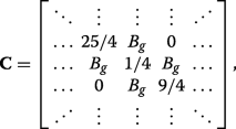
$$ \left[ 1 -\eta_{n,\frac{1}{2}}^{(e)} -\frac{\xi}{2}(p+1) \right]\widetilde{b}^{(n)}_{1} +\frac{\xi}{2}(p+3)\widetilde{b}^{(n)}_{3}=0 $$ (11a) $$ {}{\begin{aligned} &\frac{\xi}{2}(p-2l+1)\widetilde{b}^{(n)}_{2l-1}+\left[(2l+1)^{2} -\eta_{n,\frac{1}{2}}^{(e)}\right]\widetilde{b}^{(n)}_{2l+1}\\&\quad + \frac{\xi}{2}(p+2l+3)\widetilde{b}^{(n)}_{2l+3}=0. \qquad (l \ge 1) \end{aligned}} $$ (11b)Consider then Eqs. (8c) and (9b) for the q =0 solutions. The series solutions (7a) and (7b) can clearly be made to terminate if p is 0 or an even positive integer. The resulting polynomials are referred to as Ince polynomials. The remaining solutions for higher eigenvalues are simultaneously double degenerate and correspond to the energy crossings observed at q =0 for certain parameters. The existence of these degeneracies can be seen by looking at the diagonalizable matrices describing the recursion relations for a l 그리고 b l :
$$ \boldsymbol{\mathcal{A}} =\left[ \begin{array}{ccccc} 0 &\xi\left(\frac{p}{2} +1 \right) &0 &0 &\hdots \\ \xi p &4 &\xi\left(\frac{p}{2} +2 \right) &0 &\hdots \\ 0 &\xi\left(\frac{p}{2} - 1 \right) &16 &\xi\left(\frac{p}{2} +3 \right) &\hdots \\ \vdots &\vdots &\vdots &\vdots &\ddots \end{array} \right]\!, $$ (12)그리고
$$ \boldsymbol{\mathcal{B}} =\left[ \begin{array}{ccccc} 4 &\xi\left(\frac{p}{2} +2 \right) &0 &0 &\hdots \\ \xi\left(\frac{p}{2} - 1 \right) &16 &\xi\left(\frac{p}{2} +3 \right) &0 &\hdots \\ 0 &\xi\left(\frac{p}{2} -2 \right) &36 &\xi\left(\frac{p}{2} +4 \right) &\hdots \\ \vdots &\vdots &\vdots &\vdots &\ddots \\ \end{array} \right]\! $$ (13)각기. Either of the above tridiagonal matrices can be broken into tridiagonal sub-matrices if a leading off-diagonal matrix element is equal to zero, i.e. if p is an even number. The matrices will decompose into two tridiagonal blocks, one smaller finite matrix \(\boldsymbol {\mathcal {A}_{1}}\) (\(\boldsymbol {\mathcal {B}_{1}}\)) and a remaining infinite matrix \(\boldsymbol {\mathcal {A}_{2}}\) (\(\boldsymbol {\mathcal {B}_{2}}\)). From the theory of tridiagonal matrices the corresponding eigenvalue spectra for each matrix is then \(\eta (\boldsymbol {\mathcal {A}}) =\eta (\boldsymbol {\mathcal {A}_{1}}) \cup \eta (\boldsymbol {\mathcal {A}_{2}})\) and \(\eta (\boldsymbol {\mathcal {B}}) =\eta (\boldsymbol {\mathcal {B}_{1}}) \cup \eta (\boldsymbol {\mathcal {B}_{2}})\). The smaller finite matrices are analytically diagonalizable in principle, giving exact eigenvalues, and their corresponding finite length eigenvectors define the fourier coefficients yielding Ince polynomials via Eq. 7. We can see that for a given even integer p , the remaining infinite tridiagonal matrices are the same \(\boldsymbol {\mathcal {A}_{2}}=\boldsymbol {\mathcal {B}_{2}}\equiv \boldsymbol {\mathcal {D}}\) which results in the double degenerate eigenvalues. To be clear, we provide an example of when p =2 in the Appendix.
In the same way, when p is a positive odd integer the series solutions (7c) and (7d) can be made to terminate, and the matrices corresponding to \(\widetilde {a}_{l}\) and \(\widetilde {b}_{l}\) share eigenvalues resulting in the closing of higher subbands at the edge of the Brillouin zone q =± 1/2. From the definitions of the auxiliary parameters in Eq. 6, we have
$$ A_{g} =(p+1)\sqrt{B_{g}}, $$ (14)which defines the condition for exactly-solvable solutions for the lower lying solutions and simultaneously the existence of higher double degenerate eigenvalues above the p th subband, with p =0 or an even positive integer corresponding to crossings at the centre of the Brillouin zone, while crossings at the edge require p to be an odd positive integer. Figure 4b plots the size of the band gap between the first and second subbands \(\Delta \varepsilon _{12}^{(q=0)}/\varepsilon _{0}(\rho)\) as a function of A g 그리고 B g , with the dot-dashed red contour line corresponding to Eq. 14 for p =0. The schematic indicates the appropriate eigenstates of the isolated DQW at the p =0 resonance.
The application of a small transverse field C ⊥ breaks the reflection symmetry of the system, permitting hybridization of the localized well states of the isolated DQW which results in a significant change at points of degeneracy, as can be seen by comparing the schematic depicted in Fig. 4b with that in c (see also inset of Fig. 3b). We plot in Fig. 4c the behaviour of the band gap between the first and second subbands as a function of A g 및 C ⊥ . Here we see that the band gap is more sensitive to C ⊥ due to the significant change in the isolated DQW eigenstates by lowering one barrier with respect to the other. This behaviour is notably the converse of the parameter sensitivity for the band gap between the ground and first subbands. By degenerate perturbation theory, it can be shown that this induced band gap is linear in C ⊥ for the lowest crossing bands when p =0, and to higher order with increasing p . Finally, within the vicinity of the crossings, e.g. for small q about q =0 in Fig. 3a, the dispersions could be approximated as a quasi-relativistic linear dispersion yielding Dirac-like physics, which could permit superfluiditiy [81] for example. The advantage in using nanohelices lies in introducing such phenomena to portable nanostructure based devices, while also exhibiting unusual responses of the charge carriers to circularly polarized radiation [44, 45, 82–85] (or indeed magnetic fields [86, 87]) due to the helical spatial confinement.
In order to understand how our double-gated nanohelix system interacts with electromagnetic radiation, we study the inter-subband momentum operator matrix element \(T^{g\rightarrow f}_{j} =\langle {f}|\boldsymbol {\hat {j}} \cdot \boldsymbol {\hat {P}}_{j} |{g}\), which is proportional to the corresponding transition dipole moment, and dictates the transition rate between subbands ψ f and ψ g . Here, \(\boldsymbol {\hat {j}}\) is the projection of the radiation polarization vector onto the coordinate axes (j =x,y ,z ) and the respective self-adjoint momentum operators are [44, 45, 82–84]
$$ \boldsymbol{\hat{P}}_{x} =\boldsymbol{\hat{x}}\frac{i \hbar R}{\rho^{2} +R^{2}}\left[\sin(\varphi)\frac{d}{d\varphi} + \frac{1}{2}\cos(\varphi) \right], $$ (15a) $$ \boldsymbol{\hat{P}}_{y}=-\boldsymbol{\hat{y}}\frac{i \hbar R}{\rho^{2} +R^{2}}\left[\cos(\varphi)\frac{d}{d\varphi} - \frac{1}{2}\sin(\varphi) \right], $$ (15b) $$ \boldsymbol{\hat{P}}_{z}=-\boldsymbol{\hat{z}}\frac{i \hbar \rho}{\rho^{2} +R^{2}}\frac{d}{d\varphi}. $$ (15c)In terms of the dimensionless position variable φ , we are required to evaluate \(T^{g\rightarrow f}_{j} =\rho \int _{0}^{2\pi N}\psi _{f}^{\ast } P_{j} \psi _{g} d\varphi \), and upon substituting in from Eq. 4 we find
$$ {\begin{aligned} T^{g\rightarrow f}_{x} &=\frac{i \hbar R}{2\left(\rho^{2} + R^{2} \right)}\sum_{m} c_{m}^{\ast (f)} \left[ c_{m-1}^{(g)} \left(q+m-\frac{1}{2}\right)\right.\\ &\quad\left.-c_{m+1}^{(g)} \left(q+m+\frac{1}{2}\right) \right], \end{aligned}} $$ (16a) $$ {\begin{aligned} T^{g\rightarrow f}_{y} &=\frac{\hbar R}{2\left(\rho^{2} + R^{2} \right)}\sum_{m} c_{m}^{\ast (f)} \left[ c_{m-1}^{(g)} \left(q+m-\frac{1}{2}\right)\right.\\&\left.\quad+c_{m+1}^{(g)} \left(q+m+\frac{1}{2}\right) \right], \end{aligned}} $$ (16b) $$ T^{g\rightarrow f}_{z} =\frac{\hbar \rho}{\left(\rho^{2} + R^{2} \right)} \sum_{m} c_{m}^{\ast (f)} c_{m}^{(g)} (q+m). $$ (16c)We see from Eqs. 16a and 16b that light linearly polarized transverse to the helix axis couples coefficients with angular momentum differing by unity Δ 나 =± 1, whereas from Eq. 16c, linear polarization parallel to the helix axis couples only Δ 나 =0. In Fig. 5, we plot the absolute square of the momentum operator matrix element between the lowest three bands for linearly polarized light propagating perpendicular to the helix axis (i.e. with z -편극). Initially, for A g =C ⊥ =0, transitions between the ground and first bands are forbidden (as is to be expected for a unit cell with two equivalent wells resulting in a doubling of the first Brillouin zone, so it is in fact the same band). As the strength of the doubled period potential A g is increased with respect to B g , transitions become allowed away from q =0 as can be seen from Fig. 5a (following behaviour from the dotted red curve through to the solid blue curve). The parameters are swept through a resonance as we go from the solid to the dashed blue curve, wherein the situation changes drastically. To understand this behaviour, we must consider the special case of q =0. As we traverse this resonance, the energy of the Bloch function with q =0 constructed from the first excited state of the deeper well in the DQW unit cell (p -like) passes below the Bloch function constructed from the ground state in the shallower well (s -like). Consequently, the parity with respect to φ (which is a good quantum number only for q =0 or |q |=1/2) of the two excited states is exchanged resulting in the rapid switch from forbidden to allowed at q =0, wherein the z -polarized inter-subband matrix element becomes non-zero due to the operator \(\boldsymbol {\hat {P}}_{z}\) (see Eq. 15c) now coupling the even ground state with the odd first excited state. We therefore see the opposite behaviour for transitions between the ground and second band in Fig. 5b about q =0. While initially increasing A g allows transitions at q =0 between the ground state and the second excited state when it is p -like, beyond resonance (when the order of the s -like and p -like excited states are swapped) transitions are suppressed. See for example Ref. [88] for a clear picture of this interchange between the ordering of the even and the odd parity excited states. For transitions between the first and second band (Fig. 5c), we observe a large transition centred about q =0 due to the lifting of the m =± 1 degenerate states of the field-free helix by the superlattice potential. The presence of symmetry-breaking C ⊥ ruins the pristine parities of the states at the centre of the Brillouin zone and all transitions are allowed, as shown in the insets of Fig. 5.

Square of the dimensionless momentum operator matrix element between the g th and f th subbands in the first Brillouin zone as a function of the dimensionless wave vector q of the electrons photoexcited by linearly z -polarized radiation and for a variety of parameter combinations spanning the first incident of resonance. The different blue curves keep A g =0.5 and C ⊥ =0 fixed and vary B g =0.1, 0.2, and 0.3 corresponding to dot-dashed, dashed, and solid. The different red curves keep B g =0.3 and C ⊥ =0 fixed while varying A g =0.05, 0.1 and 0.3 as dot-dashed, dashed, and solid, while the dotted blue (dotted red) plots the limiting case A g =0.5 &B g →0 (A g →0 &B g =0.3). 아 Transitions between the ground and first bands. The inset plots the behaviour for fixed A g =0.5 and changing B g crossing the resonant condition at B g =0.25 (see text) in a reduced q -range, ranging from upper blue B g =0.245, lower blue B g =0.249, upper purple B g =0.251, to lower purple B g =0.255. The dashed green curves are for small non-zero transverse field C ⊥ =0.05 ranging from B g =0.245 (upper curve) to B g =0.255 (lower curve) in increments of 0.05. ㄴ Plots transitions between the ground and second bands, the inset plots the behaviour close to resonance when A g =0.5; blue is B g =0.249, purple is B g =0.251, and dark green is at resonance with C ⊥ =0.05. ㄷ Plots transitions between the first and second bands, the parameters for the inset are the same as those in (b )
In Fig. 6, we plot the absolute square of the momentum operator matrix element for right-handed circularly polarized light which propagates along the helix axis, given by |T x +iT 와 | 2 . Notably, we observe a large anisotropy between the two halves of the first Brillouin zone, while the result for left-handed polarization is a mirror image to what we see in Fig. 6. Physically, this can be attributed to the conversion of the photon angular momenta to the translational motion of the free charge carriers projected onto the direction of the helix axis, with an unequal population of the excited subband in a preferential momentum direction controlled by the relative handedness of both the helix and the circular polarization of light. An intuitive mechanical analogue would be the rotary motion of Archimedes’ screw being converted into the linear motion of water along the direction of the screw axis dictated by the handedness of the thread. As such, our system of a double-gated nanohelix irradiated by circularly polarized light exhibits a photogalvanic effect, whereby one can choose the net direction of current by irradiating with either right- or left-handed circularly polarized light [44, 45, 89]. This differs from conventional one-dimensional superlattices, wherein the circular photogalvanic effect stems from the spin-orbit term appearing in the effective electron Hamiltonian and is consequently a weaker and hard-to-control phenomenon [90, 91]. The electric current induced by promoting electrons from the ground subband to an excited subband f via the absorption of circularly polarized light can be understood from the equation for the electric current contribution from the f th subband
$$ j_{f} =\frac{e}{2 \pi \rho} \int dq \left[ v_{f}(q) \tau_{f}(q) - v_{g}(q) \tau_{g} (q) \right] \Gamma_{CP}^{g \rightarrow f}(q), $$ (17)
Square of the dimensionless momentum operator matrix element between the g th and f th subbands in the first Brillouin zone as a function of the dimensionless wave vector q of the electrons photoexcited by right-handed circularly polarized radiation |T x +iT 와 | 2 and for a variety of parameter combinations spanning the first incident of resonance. 아 The blue curves denote transitions between the ground and first band while the red curves denote transitions between the ground and second band, both with the following parameters:A g =0.5 and B g =0.3 for solid curves, A g =0.5 and B g =0.1 for dashed curves, A g =0.3 and B g =0.3 for dot-dashed curves, and A g =0.01 and B g =0.3 for dotted curves (as A g →0 the maximum of the 0→2 increases rapidly as it approaches q =− 1/2). The inset plots the behaviour as B g is tuned through resonance for A g =0.5; dotted is B g =0.24, dot-dashed is B g =0.25, and dashed is B g =0.26. The solid purple (orange) curve denotes transitions between the ground and first (second) band at resonance with C ⊥ =0.05 applied. ㄴ Plots transitions between the first and second bands. The different blue curves keep A g =0.5 fixed and vary B g =0, 0.2, and 0.3 corresponding to dotted, dot-dashed, and solid. The different red curves keep B g =0.3 fixed while varying A g =0.05, 0.1, and 0.3 as dotted, dot-dashed, and solid. We have omitted plots for C ⊥ ≠0 here as it yields no great qualitative change to the matrix elements
where \(v_{g,f}(q)=(\rho /\hbar)\partial \varepsilon _{g,f}/\partial q \) is the antisymmetric electron velocity v (q )=− v (− q ) (which we can deduce from the symmetric dispersion curves), τ g,f (q ) is a phenomenological relaxation time, and \(\Gamma _{CP}^{g \rightarrow f}(q)\) is the transition rate resulting from the optical perturbation of the electron system. Given that \(\Gamma _{CP}^{g \rightarrow f}(q) \propto |T_{x}^{g \rightarrow f} + i T_{y}^{g \rightarrow f}|^{2}\) for right-handed circularly polarized light where T x 그리고 T 와 are given by Eqs. 16a and 16b, respectively. The anisotropy present in Fig. 6a enters Eq. 17 to yield a non-zero photocurrent. This current flows in the opposite direction for left-handed polarization. Such a circular photogalvanic effect is also exhibited in chiral carbon nanotubes under circularly polarized irradiation [92, 93], although tunability predominantly stems from manipulating the nanotube physical parameters, which are hard to control. The double-gated nanohelix system offers superior versatility by fully controlling the landscape of the superlattice potential, which can be used to tailor the non-equilibrium asymmetric distribution function of photoexcited carriers (as shown in Fig. 6 for inter-subband transitions between the three lowest subbands).
On a side note, we expect that (as with chiral carbon nanotubes [93–95]) the application of a magnetic field along the nanohelix axis can take up the role played by circularly polarized radiation, whereby the current is induced by a magnetic-field-induced asymmetric energy dispersion—which in turn produces an anisotropic electron velocity distribution across the two halves of the Brillouin zone.
In summary, we have shown that the system of a nanohelix between two aligned gates modelled as charged wires is a tunable binary superlattice. The band structure for this system exhibits a diverse behaviour, in particular revealing energy band crossings accessible via tuning the voltages on the gates. The application of an electric field normal to the plane defined by the gates and the helix axis introduces an additional parameter with which to open a band gap at these crossings. Engineering the band structure in situ with the externally induced superlattice potential along a nanohelix provides a clear advantage over conventional heterostructure superlattices with a DQW basis [96, 97]. Both systems can be used as high-responsivity photodetectors, wherein tailoring the band structure (to the so-called band-aligned basis [98–100]) can lead to a reduction in the accompanying dark current. Here control over the global depth of the quantum wells also permits versatility over the detection regime, which can lie within the THz range. We have also investigated the corresponding behaviour of electric dipole transitions between the lowest three subbands induced by both linearly and circularly polarized light, which additionally allows this system to be used for polarization sensitive detection. Finally, the ability to tune the system such that a degenerate excited state is optically accessible from the ground state, along with the inherent chirality present in the light-matter interactions, may make this a promising system for future quantum information processing applications [101]. It is hoped that with the advent of sophisticated nano-fabrication capabilities [102], fully controllable binary superlattice properties will be realized in a nanohelix and will undoubtedly contribute to novel optoelectronic applications.
Here, we show using matrix algebra that in the picture of a binary superlattice pairs of subbands touch at the Brillouin zone edges if A g =C ⊥ =0 and B g ≠0, as seen from the solid blue curves in Fig. 3a. Equation 5 is equivalent to the following N -by-N pentadiagonal matrix Hamiltonian with zeros on the leading sub- and superdiagonals:
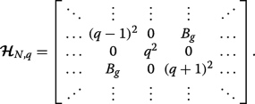 (18)
(18) Let us consider q =1/2 (we could alternatively take q =− 1/2) which makes the leading diagonal symmetric. We can then express this matrix Hamiltonian \(\widetilde {\mathcal {\boldsymbol {H}}}_{N} \equiv \boldsymbol {\mathcal {H}}_{N,q=1/2} \) in block form as
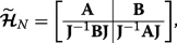 (19)
(19) 어디
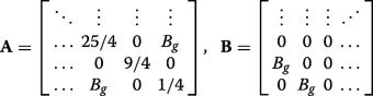 (20)
(20) are both of dimension N /2-by- N /2, and J is the exchange matrix. We may construct a matrix via permuting \(\boldsymbol {\mathcal {H}}_{N}\) with the N -by-N permutation matrix \(\boldsymbol {\mathcal {P}}_{N}\),
$$ \boldsymbol{\mathcal{P}}_{N} =\left[ \begin{array}{cccccc} 1 &0 &\hdots &\hdots &\hdots &0 \\ 0 &\hdots &\hdots &\hdots &\hdots &1 \\ 0 &1 &\hdots &\hdots &\hdots &0 \\ 0 &\hdots &\hdots &\hdots &1 &0 \\ \vdots &&&&&\vdots \\ 0 &\hdots &\hdots &1 &\hdots &0 \\ \end{array} \right], $$ (21)such that the permutation-similar matrix is
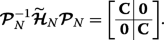 (22)
(22) Hence, the eigenvalues of \(\boldsymbol {\mathcal {P}}_{N}^{-1}\widetilde {\boldsymbol {\mathcal {H}}}_{N} \boldsymbol {\mathcal {P}}_{N}\), which are the same as the eigenvalues \(\widetilde {\boldsymbol {\mathcal {H}}}_{N}\), are double degenerate with the values given by the eigenvalue spectrum of the tridiagonal matrix C
 (23)
(23) which can also be expressed succinctly in terms of the previously defined matrices via \(\mathbf {C}=\boldsymbol {\mathcal {P}}_{N/2}^{-1}\mathbf {A}\boldsymbol {\mathcal {P}}_{N/2}+\boldsymbol {\mathcal {P}}_{N/2}^{-1}\mathbf {B}\mathbf {J}\boldsymbol {\mathcal {P}}_{N/2}^{4}\). We can see that applying C ⊥ ≠0 (inset of Fig. 3a) or both C ⊥ 그리고 A g ≠0 (inset of Fig. 3b) ruins the symmetry in the matrix Hamiltonian and prevents the existence of eigenvalues with multiplicity beyond unity, resulting in the appearance of band gaps.
As an example, let us specifically consider the case where p =2, wherein the matrices (12) and (13) become:
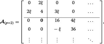 (24)
(24) 그리고
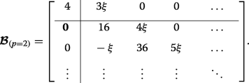 (25)
(25) This case corresponds to the crossings of the blue curves at the edge of the Brillouin zone in Fig. 3d (whereas p =0 results in crossings at q =0 in Fig. 3b). The lower eigenvalues are found exactly by diagonalizing each of the two finite matrices and they interlace, yielding \(\eta _{0,1,2} =2-\sqrt {4+4\xi ^{2}}, 4, 2+\sqrt {4+4\xi ^{2}}\). The infinite lower-right-hand block tridiagonal matrices coincide, thus the remaining double degenerate eigenvalues are found by approximately or numerically solving Det[D −η I ]=0.
The data for the figures all stem from numerically diagonalizing the matrix described by Eq. 5 and can readily be achieved in any numerical software package. With this in mind, the datasets used and/or analyzed during the current study are available from the corresponding author on reasonable request.
나노물질
초록 본 논문에서는 도핑이 없는 핀형 SiGe 채널 TFET(DF-TFET)를 제안하고 연구한다. 고효율 도핑 없는 라인 터널링 접합을 형성하기 위해 핀 모양의 SiGe 채널과 게이트/소스 중첩이 유도됩니다. 이러한 방법을 통해 높은 온 상태 전류, 12자리의 스위칭 비율 및 명백한 양극성 효과가 없는 DF-TFET를 얻을 수 없습니다. 높은 κ DF-TFET의 오프 상태 누설, 인터페이스 특성 및 신뢰성을 개선하기 위해 재료 스택 게이트 유전체가 유도됩니다. 또한, 도핑이 없는 채널과 핀 구조를 사용하여 도핑 프로세스의 어려
구성품 및 소모품 Arduino UNO × 1 spdt 전환 × 7 M3 x 8 소켓 헤드 캡 나사 × 15 M3 너트 × 3 Adafruit Standard LCD - 파란색 바탕에 16x2 흰색 × 1 40mm 스탠드오프 × 4 Adafruit 실리콘 커버 연선 - 30AWG 여러 색상 × 1 스위치 드레스 너트 1/4-40 선택 사항입니다. × 9 흰색 LED 링이 있는 견고한