

나노물질

산업 제조
섬유는 어디에나 있으며 일반적으로 수동적입니다. 광섬유로 구현된 광전자공학은 생합성 및 웨어러블 전자공학, 환경 감지 및 에너지 수확을 비롯한 여러 응용 분야에 혁명을 일으킬 수 있습니다. 그러나 섬유에 고성능 전자 장치를 구현하는 것은 실리콘과 같은 결정질 반도체로 만들어진 장치를 질서 정연하고 주소 지정이 가능한 섬유로 포장할 수 있는 재료 처리 전략이 어렵기 때문에 여전히 어려운 과제로 남아 있습니다. 확장 가능한 방식. 현재의 광섬유 센서 제조 방식은 확장 불가능하거나 전자 성능이 실리콘보다 열등한 칼코겐화물 유리와 같은 비정질 반도체로 반도체 선택을 제한하여 표준 실리콘과 비교할 때 이러한 센서의 대역폭과 감도가 제한적입니다. 포토다이오드. 우리 그룹은 현대 마이크로프로세서의 출현을 가능하게 한 VLSI(Very Large-Scale Integration)와 유사한 논리 회로 및 감각 시스템의 보편적인 섬유 내 제조를 입증합니다. 우리는 실리카, 실리콘 및 고온 금속의 통합 마이크로 전자 장치 및 시스템에 일반적인 섬유 내 재료 아키텍처를 조립하는 다목적 하이브리드 제조 방법론을 개발합니다. "섬유용 VLSI" 또는 "VLSI-Fi"라고 하는 이 방법은 재료 선택적인 공간적으로 일관된 모세관 분해를 통해 예비 성형체의 3D 인쇄, 섬유의 열 인발 및 섬유 내장 통합 장치의 인발 후 조립을 결합합니다. 섬유 코어의. 우리는 이 방법이 새로운 차원의 내구성, 저비용, 보급형 섬유 장치 및 센서를 제공하여 가구 및 의류와 같은 인간이 만든 물체와 만나는 직물을 사물 인터넷(IoT)에 통합할 수 있다고 믿습니다. 또한 3D 프린팅의 혁신을 촉진하여 디지털 제조 방식을 나노전자공학 영역으로 확장할 것입니다.
유리 인발 섬유는 로마 시대로 거슬러 올라가지만 최초의 기능성 광섬유는 1792년 프랑스의 Chappe 형제가 통신 목적으로 제조했습니다[1]. 1842년 스위스의 물리학자인 Jean-Daniel Colladon은 물분사를 통해 빛이 내부로 안내될 수 있음을 보여주었습니다[2]. 이 두 가지 발견은 수십 년에 걸친 광학 및 재료 엔지니어링 개선을 통해 오늘날의 효율적인 섬유로 이어지며 25,000km 길이의 태평양 횡단 해저 케이블(TPC) 완성과 같이 전 세계 수 킬로미터에 걸쳐 고속 통신 및 데이터 저장을 가능하게 합니다. 1996년 [3, 4]. 또한 광섬유 센서(FOS)는 생물의학, 석유 및 가스, 해양, 건축, 화학, 항공우주 등 다양한 분야에 사용됩니다[5, 6].
Philip Russel이 1996년에 개발한 광결정 섬유(PCF)를 사용한 광 전파의 제어 및 개선된 성능은 보다 복잡한 섬유 내부 기능 구조에 대한 연구의 문을 열었습니다[7,8,9]. 새로운 미세구조는 전자공학[12], 광전자공학[11], 섬유내 합성[13], 미세유체공학[14], 미세전자기계 시스템[15, 16] 및 생합성 인터페이스 [17]. 스마트 섬유는 광통신을 넘어서는 비전통적인 기능과 상업용 직물에서 섬유의 일반적인 사용을 포함한다는 점에서 기존의 섬유와 다릅니다. 스마트 섬유는 미세 구조의 광학 간섭으로 인한 섬유의 색상 외관을 제어함으로써 전자 섬유의 심미성을 위해 사용될 수 있거나 [18] 광 안내를 허용하는 기존의 광섬유 가이드 및 유전체 미러 라이닝의 경우와 같이 성능을 향상시키는 데 사용할 수 있습니다. 공기를 통해 [19, 20].
섬유를 기능적으로 만들기 위해서는 다양한 전자적 특성을 가진 재료로 구성되어야 하고, 그 아키텍처는 주어진 기능을 수행하도록 특별히 설계되어야 하며, 내부 기능은 현재 통신의 핵심보다 수십 배 작은 나노 스케일로 축소되어야 합니다. 섬유. 섬유는 일반적으로 광섬유 제조 방법, 즉 "프리폼(preform)"이라고 하는 거시적 원통형 또는 직육면체 막대에서 열로 당겨서 만들어집니다. 제조 공정은 금속, 절연체 및 반도체와 같은 적절한 코어 및 클래딩 재료를 선택하는 것으로 시작됩니다. 예를 들어, 금속-절연체-반도체 구조를 포함하는 최초의 섬유는 광검출을 위해 2004년에 개발되었습니다[21]. 프리폼의 재료는 점도가 μ가 되도록 선택됩니다. , 4
본질적으로 섬유의 확대 버전인 프리폼은 그림 1a와 같이 깔개와 같은 재료의 롤링, 퍼즐과 같은 밀링 부품 쌓기 또는 3D 인쇄와 같은 다양한 기술을 사용하여 만들 수 있습니다. (I) 이 리뷰에서 논의한 다음 진공 소결로 통합합니다. 그런 다음 예비 성형품은 노에서 가열되어 카라멜 또는 태피와 같은 섬유로 늘어납니다(그림 1a(II)의 드로잉 원뿔 참조). 이때 점도, 경계면과 같은 구성의 주어진 열기계적 특성을 기반으로 단면 배열을 유지합니다. 에너지, 상호 접착 및 차등 열팽창(그림 1a(III)) [22]. 3D 인쇄된 프리폼의 경우 이 프로세스는 그림 1a에 개략적으로 설명되어 있습니다. 일반적인 드로우는 약 5 nm의 매우 미세한 나노스케일 단면 직경을 가진 수 킬로미터의 섬유를 생성할 수 있습니다[23, 24].
<그림>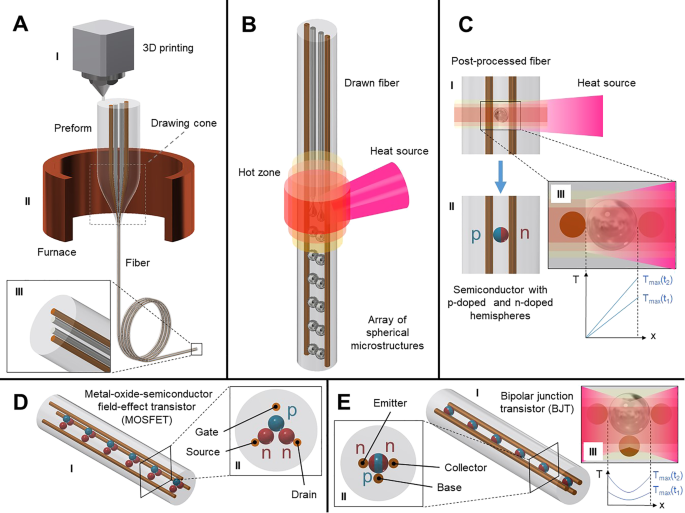
VLSI-Fi:"2D + 1D + 0D" 접근 방식을 나타내는 VLSI-Fi 기술의 개념적 개략도. 3D 인쇄 프리폼 a (I) 열 연신 a (II) 프리폼(2D)의 단면 형상을 보존하는 길고 가는 섬유로. ㄴ 공간적으로 일관된 재료 선택적인 모세관 분해(+1D)를 통한 섬유의 축 방향 패터닝으로 초기에 연속적인 별도의 코어를 병렬로 접촉된 개별 장치의 어레이로 조립합니다. ㄷ 분리 후 반도체 입자의 도핑에 대한 분리 기반 제어를 통해 개별 장치의 내부 아키텍처를 제어할 수 있습니다. c (II) 열 구배 c를 통해 (Ⅲ). d (I) VLSI-Fi를 통한 금속 산화물 반도체 전계 효과 트랜지스터(MOSFET)의 개략도. 여기서 p형 및 n형 반도체는 각각 파란색과 빨간색으로 표시됩니다. 실리카 섬유에 내장된 황금색 연속 막대는 게이트, 소스 및 드레인 역할을 합니다. 결과 섬유 단면은 d에 표시됩니다. (II). 마찬가지로 (I) VLSI-Fi에 의해 구현된 바이폴라 접합 트랜지스터(BJT)의 개략도를 보여줍니다. 섬유 단면 e (II) n-p-n 접합의 p형 및 n형 반도체가 각각 파란색과 빨간색으로 표시된 BJT(섬유에 내장된 연속 막대)의 에미터, 컬렉터 및 베이스를 보여줍니다.
포스트 드로잉 단계에서 모세관 불안정성을 이용하여 섬유를 재액화하여 공간적으로 일관된 재료 선택적인 방식으로 코어를 분해할 수 있으므로 섬유 내장 구조에 대한 축 제어가 가능합니다[25,26, 27] 도 1b에 도시된 바와 같이. 축 방향으로 코어를 패터닝하기 위한 대체 기술에는 광중합 코어의 포토마스크를 통한 UV 노출이 포함되며, 그 결과 사소한 모양의 미세 입자가 생성됩니다[28]. 다른 하이브리드 기능화 기술에는 섬유 표면을 기능성 물질로 코팅하고[10, 29] 표준 CMOS(Complementary Metal-Oxide-Semiconductor) 제조에 의해 제조된 광전자 장치 어레이에 드로우[12]에 의해 섬유 클래딩을 제한하는 것이 포함됩니다.
섬유는 개별 섬유의 기능을 능가하는 집합적 기능을 얻기 위해 직물이나 망으로 직조될 수 있습니다[30]. 생체 모방을 통해 설계된 섬유는 자연의 유용한 특성에 따라 모양을 만들어 소수성과 같은 직물의 기능을 향상시킬 수 있습니다[31]. 섬유는 또한 실리카 피복 섬유[13] 또는 상 분리에 의한 다공성 구조의 열 유도 제조[32]에서 알루미늄 코어를 실리콘으로 변환하는 것과 같은 저렴한 재료 생산을 위한 합성 플랫폼으로 생각할 수 있습니다. 섬유는 또한 위험한 휘발성 물질의 환경 화학 감지와 같은 원격 및 분산 신호 감지를 제공할 수 있습니다[29]. 섬유 설계의 유연성은 신경퇴행성 질환 연구를 위한 마우스의 깊은 척수피질 자극 및 모니터링과 같은 복잡한 응용 분야를 위해 여러 기능적 양식을 하나의 섬유에 통합할 수 있는 정도입니다[33]. 이러한 예는 스마트 섬유가 자연적인 솔루션인 다양한 영역 중 일부를 보여줍니다.
섬유는 보편적으로 어디에나 있지만 얇은 섬유 내에 고성능 마이크로 전자 시스템을 통합하는 것은 여전히 주요 과제입니다[11, 12]. 이 문제를 해결하는 다양한 접근 방식이 제안되었으며 주로 저온 재료에 중점을 두었습니다. 예를 들어, 고압 화학 기상 증착(HPCVD)은 화합물 반도체를 미세구조 광섬유(MOF)[34]에 통합하고 유연한 실리콘 p-i-n 접합 섬유[35]를 만드는 데 사용되었습니다. 또는 CO2 레이저는 실리카 섬유의 SiGe 코어를 재결정화하여 전기적 특성을 조작하는 데 사용되었습니다[36]. 이러한 접근 방식은 본질적으로 무정형이거나 본질적으로 확장할 수 없는 칼코겐화물 물질의 경우와 같이 제한된 전자 대역폭을 가진 장치를 초래합니다.
이와 같이 Fibers and Additive Manufacturing Enabled Systems Laboratory(FAMES Lab)는 이 리뷰에서 설명하는 섬유의 3D 아키텍처를 제어하는 기술을 개발하여 현재 구현하고 있습니다. 최종 섬유의 복잡함은 프리폼 단면의 복잡성과 상관 관계가 있기 때문에 프리폼의 자유 형태 제작은 다른 방법으로는 얻을 수 없는 섬유 장치 기능을 가능하게 합니다. 또한 3D 프린팅은 널리 접근할 수 있어 전통적으로 사용되는 방법에 대한 비용 효율적이고 사용자 친화적인 기술 대안이 되며, 열가소성 수지에서 고온 재료 및 생체 재료에 이르기까지 광범위한 재료를 허용합니다[37].
또한 FAMES Lab은 적층 제조에서 열가소성 플라스틱을 사용하는 전통적인 방법과 함께 고온 재료를 처리할 수 있는 능력을 갖추고 있어 Si/Ge[38]의 높은 전자 이동성과 같은 특성을 활용할 수 있습니다. 납 지르콘 티탄산염(PZT)/BaTiO3의 향후 사용 폴리머에 비해 큰 압전 계수를 갖고 [39, 40] 더 높은 음향 대역폭[41]을 갖는 압전 응용을 위한 복합 재료.
이러한 과제를 염두에 두고 우리는 더 빠르고 복잡한 프리폼 제작을 달성하기 위해 적층 제조를 사용하는 최적화 솔루션, 섬유의 축 제어를 최적화하기 위한 모세관 분해 시뮬레이션, 섬유와 조직 공학의 조합을 제안합니다. 이러한 전략을 통해 유망한 섬유 장치 응용 프로그램 중 하나로 시험관 내 약물 및 치료 분석을 위한 생체 감지 및 생체 기능화 기능을 갖춘 현실적인 생체 의학 플랫폼을 만들 수 있습니다.
기능성 섬유를 실현하기 위해 우리는 VLSI(Very Large-Scale Integration)에서 영감을 얻었습니다. 이는 1970년대에 현대적인 마이크로프로세서를 탄생시킨 디지털 설계 및 제조 기술입니다. 이 기술은 반도체 기판 웨이퍼의 노출된 영역에 대한 포토리소그래피 및 화학적/열적 처리를 사용하여 이 층(2D)에서 집적 회로의 특징을 정의하는 한편, 완전한 회로의 제조는 수직 방향으로 이러한 개별 층을 적층함으로써 진행됩니다. 웨이퍼 표면(+1D). 또한 회로의 개별 구성 요소(+0D)의 전자 도핑은 주입 및 열 활성화에 의해 제어될 수 있습니다[42]. "섬유용 VLSI" 또는 "VLSI-Fi"라고 하는 섬유에 대한 우리의 접근 방식은 유사합니다. 첫째, 적층 제조 및 예비 성형품의 열 인발은 섬유 장치(2D)의 단면 형상을 정의합니다. 둘째, 결과적인 섬유는 나중에 축 방향으로 패턴화될 수 있어(+1D), 처음에는 연속적이지만 분리된 코어에서 통합된 개별 장치의 어레이를 조립할 수 있습니다. 셋째, 개별 섬유 내 내장 장치(0D)의 분리 기반 구조화를 수행할 수 있습니다. 표 1은 두 기술을 비교하여 각 기술(“2D + 1D + 0D”)에 의해 가능해진 각 기하 제어 수준 간의 일치를 강조 표시합니다. 설명된 단계의 개략도는 VLSI-Fi 기술을 사용하여 가능한 섬유 내 내장 장치의 예를 실현할 수 있는 그림 1에 자세히 나와 있습니다.
이 섹션에서는 먼저 폴리카보네이트 프리폼의 3D 인쇄에 대한 작업을 설명하고 광조형을 사용한 유리 3D 인쇄의 최근 발전에 대해 설명합니다. 그런 다음 공간적으로 일관성 있고 재료 선택적인 모세관 분해를 통해 섬유의 축 방향 패터닝에 접근합니다. 이를 통해 처음에는 연속적인 개별 코어를 병렬로 접촉된 개별 장치의 어레이로 조립할 수 있습니다. 마지막으로, 생체 외에서 생존 가능한 조직 성장을 모니터링하기 위해 조직 공학과 결합된 생체 인터페이스 섬유의 적용을 제안합니다. 섬유내 미세유체 채널을 사용하여 세포를 전달하고 움직임 제어를 위한 생화학 물질 및 형상 기억 합금 와이어를 전달하고 압전 소자를 사용하여 초음파로 환경을 매핑함으로써 기능이 활성화됩니다.
앞서 언급한 바와 같이 박막 압연 및 적층 가공과 같은 기존의 프리폼 제작 기술[10]은 복잡한 기하학적 구조를 생산하는 데 한계가 있고 섬유 연신 공정에서 상당한 시간이 소요되며 숙련된 기술이 필요합니다. 노동력과 고가의 장비. 3D 프린팅은 용해성 지지 재료와 부분적으로 자동화되고 사용자 친화적인 프로세스를 통해 이러한 문제를 해결합니다. 이를 통해 비교적 짧은 시간에 매우 복잡한 형상을 쉽게 인쇄할 수 있습니다.
폴리카보네이트(Hatchbox 3D) 프리폼의 인쇄 각도의 영향을 평가하기 위해 단일 헤드 Prusa i3 MK2 FDM 프린터를 사용하여 원통형 및 사각형 막대를 인쇄했습니다. 압출기 및 프린트베드 온도는 각각 235 °C 및 105 °C로 설정되었으며 프린터는 0.35mm 노즐로 100% 충전 프리폼을 생산하도록 설정되었습니다. 프리폼의 레이어 방향은 인쇄 베드에 대한 부품의 수평 방향에 따라 달라지며, 열 인발 중에 프리폼이 퍼니스에 도입될 때 열 흐름은 레이어 방향에 영향을 받습니다. 열 연신에 가장 적합한 방향을 테스트하기 위해 0°, 15°, 30°, 45° 및 90° 방향의 프리폼을 인쇄했습니다. 모든 각도는 프리폼의 세로축과 가로축 사이에서 측정되었습니다. 3D 인쇄된 프리폼은 90 °C, 100 °C 및 200 °C의 세 가지 온도 영역이 있는 용광로에서 열 인발 과정을 거쳤습니다. 원통형 프리폼의 경우 열 인발은 0° 및 45° 각도에서 성공적이었습니다. 90° 프리폼 드로우는 레이어 박리로 인해 항상 실패합니다.
우리는 또한 그림 2a(I)와 같이 즉석 채우기 패턴이 있는 사각형 막대와 같은 비평형 구조를 성공적으로 그릴 수 있었습니다. 질서정연한 구조로 0° 정사각형 기반 프리폼 드로우는 성공적이었고 약간 변형되었지만 섬유는 여전히 프리폼의 모양을 유지할 수 있었습니다. 40 μm × 60 μm의 낮은 치수를 가진 섬유가 성공적으로 연신되었으며 층의 박리가 없는 그림 2a에 나와 있습니다. 또한 모든 레이어가 제대로 통합되었습니다. 섬유 단면의 예가 그림 2a(IV)에 표시되어 있고 어닐링 전과 후의 섬유 이미지가 각각 그림 2a(V)와 2a(VI)에 나와 있습니다. 여기서 어닐링된 섬유 향후 작업에서 특징이 될 광학적 투명도를 달성합니다. 이 실험에서 우리는 가장 성공적인 프리폼이 0°로 인쇄된 반면 90°는 인발 과정에서 항상 박리된다는 결론을 내렸습니다. 3D 인쇄 프리폼의 배향 각도가 감소함에 따라 열 연신 섬유의 레이어 통합이 향상되었습니다.
<그림>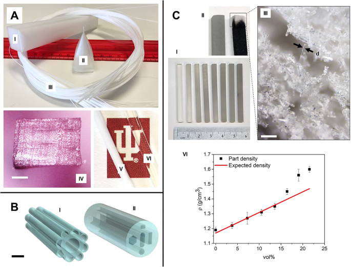
3D 인쇄 프리폼:a (I) 정사각형 기반 3D 인쇄 폴리카보네이트 프리폼. 아 (II) 원뿔 그리기. 아 (III) 열 연신 후 생성된 폴리카보네이트 섬유. 아 (IV) 층 박리가 없는 연신 공정 후의 섬유 단면. 단면은 채우기 패턴의 비등방성 다공성으로 인해 직사각형입니다(눈금 막대 200 μm). 아 (V) 어닐링 전의 인발 섬유. 아 (VI) 명백한 광학 투명도를 갖는 어닐링 후 인발된 섬유. ㄴ 고정밀 압출 기반 3D 프린팅으로 소다석회 유리에서 성공적으로 구현된 유리 프리폼의 CAD 모델. ㄴ (I) 구조는 파란색 독거미 털을 모방합니다. ㄴ (II) 비평형 단면 형상의 프리폼 모델(축척 막대 1 cm). ㄷ (I) SLA 기술로 인쇄된 유리 충전재(왼쪽에서 오른쪽으로)가 증가하는 정사각형 유리 샘플. ㄷ (II) 굽기 전(왼쪽)과 굽는 동안(오른쪽) 유리 샘플의 세부 사항. 후자의 경우 탄화된 수지의 잔류물로 인해 검은색으로 변색되는 것을 볼 수 있으며, 이러한 잔류물을 제거한 후 팁은 흰색으로 변색됩니다. ㄷ (III) 백색 착색은 상호 연결된 다공성 구조에서 압축된 밀링 섬유의 자연 색상의 결과인 ash-out 섹션(눈금 막대 200 μm)의 현미경 사진입니다. 또한 이미지에서 d로 표시된 유리 섬유의 공칭 너비는 16 μm(#38 Fiber Glast)의 예상 값과 상관 관계가 있습니다. ㄷ (IV) 인쇄된 유리 프리폼 밀도의 플롯(ρ ) 인쇄 재료의 평균 밀도와 함께 수지와 혼합된 유리 섬유의 부피 분율의 함수로서
열가소성 수지 외에도 용융 석영을 포함한 유리는 광학, 통신 및 전자 제품에서 중요한 과학 및 엔지니어링 응용 분야를 가지고 있습니다[43]. 구조화된 실리카 섬유는 예를 들어 패션용 직물의 무염색 착색, 광학-화학적 검출을 위한 광결정 섬유 또는 통신 및 빛의 긴밀한 초점을 위한 단일 모드 섬유와 같은 여러 응용 분야에 이점을 줄 수 있습니다. 이러한 섬유는 일반적으로 예비 성형품 제작 및 예비 성형품을 섬유로 열 인발하는 2단계 공정으로 제조됩니다. Draw 공정은 비교적 간단하고 저렴하지만, 이때 프리폼 제작은 케이스 바이 케이스 처리가 필요하며, 각각의 특정 프리폼 구성에 대해 별도의 기술을 개발하여 적용해야 합니다.
그림 2b는 Micron3DP가 설명하는 제품과 유사한 압출 기반 인쇄 기술에서 높은 정밀도로 성공적으로 구현된 소다석회 유리 프리폼 CAD(Computer-Aided Design) 모델을 보여줍니다[44]. 이 재료는 특히 IR과 같은 장파장에서 유망한 광학적 특성을 가지고 있어 새로운 광학 기능을 가진 섬유 제조에 흥미로운 후보가 됩니다. 그림 2b(I)에 표시된 프리폼 모델은 [46]에 제시된 구조와 유사한 파란색 독거미 털의 구조를 모방하고, 그림 2b(II)에서 프리폼 단면은 비평형 기하학을 포함하며 다음과 같습니다. 따라서 표면 장력 최소화로 인해 변형되기 쉽습니다. 이 모델은 복잡하고 비평형 프리폼 단면을 달성할 가능성을 검증하기 위해 설계되고 실현되었습니다.
클래딩 구조는 인발 과정에서 섬유에 기계적 무결성을 제공하기 때문에(가장 점성이 있는 재료로 구성됨) 지금까지 우리의 노력은 섬유의 이 구성요소에 집중되었으며 궁극적으로 단면 형상의 보존을 목표로 했습니다. 프리폼의. 장기적으로 우리는 다중 재료 압출 기술을 개발하는 것을 목표로 하며, 이를 통해 여러 재료를 동일한 인쇄물에 모놀리식으로 통합할 수 있습니다. 또는 Si 또는 Ge와 같은 분말 재료로 구조를 채우는 것이 가능합니다. 그런 다음 채워진 구조를 소결하여 프리폼을 얻을 수 있습니다. Gumennik et al. 유사한 접근 방식을 설명했습니다[47].
소다석회 유리를 코어 재료로 사용하여 섬유를 생산하는 데 관심이 있는 경우 한 가지 간단한 접근 방식은 서스펜션 코어 프리폼을 인쇄하는 것입니다. 매달린 코어 섬유는 감지[48] 및 저손실 테라헤르츠 안내[49]를 포함한 다양한 응용 분야에 관심이 있으며 일반적으로 폴리머로 실현됩니다[49]. 이러한 유형의 섬유 기하학에서 코어는 코어를 외부 레이어에 연결하는 버팀대에 의해 지지됩니다. 드로잉 후 이러한 구조는 유도된 빛의 경우 효과가 매달린 코어와 같은 방식으로 관심 파장의 차원으로 축소됩니다. Monro et al. 실리카 및 비스무트 유리와 같은 다양한 재료에서 부유 코어 섬유를 보고했습니다[48]. 또한 특히 생물학적 및 화학적 감지에서 이러한 섬유의 감지 응용 프로그램에 대한 일련의 예를 제공하여 이러한 섬유 형상의 실행 가능성을 확인합니다.
광경화성 실리카 나노복합체를 사용하여 맞춤형 수지를 사용한 광조형 기반 유리 3D 프린팅에 대한 새로운 접근 방식이 설계되었습니다[50]. 여기에서 우리는 기성 상용 수지를 기반으로 3D 프린팅으로 유리 섬유 프리폼을 제조하는 방법을 제안합니다. 이를 통해 SLA(stereolithography)를 사용하여 3D 프린팅된 유리 부품을 달성하는 비용 효과적이고 간단한 방법을 만들 수 있습니다. SLA 프린터(Formlabs의 Form 2)는 405 nm 파장의 레이저를 사용하여 작동하며 구축된 플랫폼이 층별로 증가함에 따라 통의 바닥을 통해 수지를 교차 연결합니다.
유리 인쇄물을 얻기 위해 상업용 투명 수지(Formlabs FLGPCL04 Clear)와 0.79 mm(1/32") 붕규산 유리 섬유(#38 Fiber Glast)의 혼합물을 인쇄 공정에 사용합니다. 이를 통해 인쇄 공정을 크게 제어할 수 있습니다. 최종 인쇄 재료 조성 및 섬유의 원하는 특성을 달성하기 위한 유연성 유리 섬유를 자기 교반기를 사용하여 투명한 수지에 분산시킨 유리를 소량씩 첨가하고 각 첨가 후 약 3분 동안 균질화 인쇄 공정을 위해, 4 × 4 × 50 mm 크기의 직육면체 프리폼을 90° 방향으로 인쇄한 후, 부품을 이소프로판올에 10분 동안 담가 과잉 수지를 제거했습니다. , 그리고 60 °C에서 30분 동안 UV 광으로 후 경화됩니다. 인쇄 수지에 혼합된 유리 섬유의 부피 비율이 증가하는 경화된 유리 프리폼(왼쪽에서 오른쪽으로)은 그림 2c(I)에 나와 있습니다.
그런 다음 예비 성형품은 잔류 수지를 제거하고 유리 입자를 소결하기 위해 후처리되어 전체가 유리로 구성된 부품이 됩니다. 프리폼에 대한 이러한 프로세스의 영향은 그림 2c(II)에 나와 있습니다. 그림 2c(II)에서는 경화 후(왼쪽)와 베이킹 프로세스 후(오른쪽) 프리폼을 볼 수 있습니다. 후자의 경우 회절 화덕에서 굽은 결과 검은색을 볼 수 있으며 탈지 후 끝 부분은 흰색을 나타냅니다. 그림 2c(III)은 소결 전 예비성형체를 현미경으로 촬영한 이미지를 보여줍니다. 여기에서 모든 수지가 실제로 부품에서 구워져 유리 섬유로만 형성된 상호 연결된 구조가 생성된다는 것을 알 수 있습니다. 화학 반응 및 수축을 제어하려면 베이킹 온도 및 가열 프로파일과 같은 여러 매개변수를 제어해야 합니다. 바인더의 열적 탈바인딩은 애싱 오븐을 사용하여 달성되었습니다. 생성된 갈색 부분을 고온 튜브 오븐에서 소결했습니다. 소결은 1300 °C의 온도와 5 × 10 -2 압력에서 수행되었습니다. mbar, [51]에 규정된 프로토콜을 따릅니다. 800 °C의 유지 단계는 분자 결합 물과 표면 결합 실라놀 그룹을 증발시키도록 설정되었습니다. 진공 소결은 소결 유리 부품 내부의 공기 포획을 감소시키기 때문에 광학 투명도를 향상시킵니다[52].
후처리 후, 밀도를 얻기 위해 부품의 부피와 중량을 측정합니다. 그런 다음 ρ로 계산되는 경화성 수지와 유리 섬유 혼합물로 구성된 인쇄 재료의 평균 밀도와 비교됩니다. 평균 =ρ 수지 (1 − χ v ) + ρ 유리 (χ v ), 여기서 ρ 수지 =1.17 g/cm 3 는 경화된 투명 수지의 밀도, ρ 유리 =2.55 g/cm 3 는 밀링된 유리 섬유의 밀도이고, χ v 수지에 혼합된 유리 섬유의 부피 비율입니다.
결과는 표 2와 그림 2c(IV)에 그래프로 표시되어 있습니다. 여기서 인쇄 재료의 평균 밀도와 비교하여 수지에 있는 유리 섬유의 다양한 부피 비율에 대한 인쇄 부품 밀도를 나타냅니다. 수지에 혼합된 유리의 낮은 부피 비율에 대해 얻은 결과가 예상 범위 내에 있음을 관찰했습니다. 그러나 더 높은 유리 농도에서는 이상적인 밀도의 선형 거동에서 벗어나는 것을 볼 수 있습니다. 이것은 인쇄 중 침전에 기인할 수 있으며, 이는 이러한 부피 비율에서 중요해지며, 따라서 해당 인쇄물에서 더 높은 농도의 유리를 효과적으로 생성합니다. 프린팅 공정은 탱크 바닥에서 발생하며, 프린팅하는 동안 침전으로 인해 유리 농도가 지속적으로 증가합니다. 계산된 곡선에 있어야 하는 초기 균일 농도(이상)에서 시작합니다.
표 2에서 21.54 vol% 밀링된 유리 섬유 충전 부품에서 측정된 밀도가 1.61 g/cm 3 임을 알 수 있습니다. , 이는 실제 부피 비율이 31.88 vol%임을 의미합니다. 실험 과정에서 실제 34.78 vol% 밀링 유리 섬유 충전재가 있는 샘플을 얻었습니다. 이 결과는 Kotz et al.에 의해 제작된 37.5 vol% 실리카 충전재와 멀지 않았습니다. [53], 우리가 이 작업에서 사용하는 상업용 수지와 대조적으로 맞춤형 수지가 개발된 곳입니다. 이 작업의 향후 방향에는 열처리 절차, 부품 소결 및 결과 부품의 기계적 및 광학적 특성에 대한 연구가 포함됩니다.
Preform이 열적으로 연신되면 그림 1a(III)와 같이 단면이 보존된 길고 가는 섬유가 생성됩니다. 하나 이상의 코어가 있는 섬유의 경우, 이들은 그림 3에서와 같이 공간적으로 일관성 있고 재료 선택적인 모세관 분해 과정을 통해 축 방향으로 패턴화될 수 있습니다. 무한히 균일하게 가열된 유체 실린더는 주변 유체의 영향을 고려하여 [55], 전파되는 Rayleigh 불안정성은 전면 전파의 개념을 도입합니다[56]. Liang et al.과 같은 문헌에서 모세관 불안정성의 수학적 처리에 대한 몇 가지 예를 찾을 수 있습니다. [57], 이러한 작업은 대부분 우리의 경우 적용할 수 없는 등온 요법에 중점을 둡니다. 더욱이, 우리의 경우에는 열 구배 및 이에 따른 점도 구배 전파의 추가 합병증이 있습니다. 따라서 Powers et al.에서 언급한 것처럼 한계 불안정성 기준 기반 프로세스에 더 가깝습니다. [56]. 계산 결과와 실험 결과를 결합하여 축 열 구배 현상을 통한 섬유 분해에 대한 수학적 모델을 설정하는 것을 목표로 합니다.
<그림>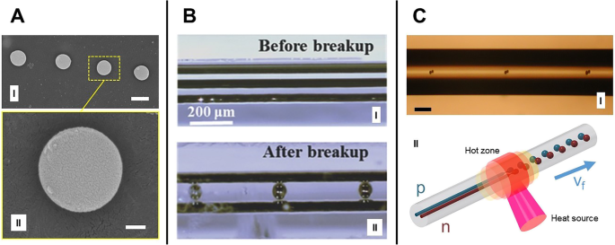
모세혈관 분해:a (I) 모세관 분해를 통해 형성된 Si 구체를 보여주는 섬유 단면(스케일 바 0.5 μm). 아 (II) Gumennik et al.의 모양 품질(스케일 막대 100 nm)을 나타내는 단일 구 이미지. [26]. ㄴ (I) b 이전 단일 실리카 섬유의 금속-반도체-금속 광검출 장치의 예 (I) 및 b 이후 (II) Wei et al.의 분해 과정. [54]. ㄷ (I) Gumennik et al.의 이중 코어 섬유를 이중 구형 클러스터(스케일 막대 100 μm)로 분해. [26]. ㄷ (II) c에 표시된 프로세스의 도식적 표현 (I), 각각 파란색과 빨간색으로 표시된 p형 및 n형 코어 사용
모세관 분해 시뮬레이션의 현재 단계는 고정 영역에 중점을 둡니다. 우리는 열 구배를 받는 초기에 고정된 섬유에서 불안정성이 어떻게 처음 발생하는지 분석하는 데 관심이 있습니다. 이 과정은 Gumennik 등이 수행한 모세관 분해 실험의 초기 단계와 유사합니다. [26], 4μm 두께의 Si 코어가 있는 실리카 섬유가 각각 0.3 및 0.1 L/min의 유량으로 수소-산소 화염의 고온 영역을 통해 공급됩니다. 이러한 유형의 토치로 도달할 수 있는 최대 온도는 최대 2800 °C에 도달할 수 있지만 섬유가 경험하는 최대 온도는 실리카 비등점인 2230 °C 미만이어야 합니다.
Considering that the flame width is between 3 and 3.5 mm and that the fiber has a diameter of about 300 μm, it is easy to understand why it is not feasible to experimentally measure the temperature gradient to which the fiber is exposed. Furthermore, the dynamic nature of the breakup process and the fact that it involves multiple materials with varying emissivities further adds to the complexity of the problem, while the fiber’s high aspect ratio and sharp viscosity ratios render the numerical simulation of the full Navier-Stokes equations computationally challenging.
In our simulations (using COMSOL Multiphysics® 5.3a, with its Microfluidics and Heat Transfer modules) shown in Fig. 4a, we assume an axisymmetric fiber with radius r fiber = 140 μm, composed of a thin Silicon core (r core = 2 μm) enclosed in a Silica cladding. Initial heat-transfer simulations showed that a fiber length of 15 mm is sufficient to ensure that the fiber extremities remain at room temperature, thus avoiding influence from the boundaries to the breakup process. Through the sweep of different parameters such as heat source length and distance to the fiber surface, as well as power, we can observe the changes produced in the breakup behavior, thus collecting information about the temperature gradient. Also of importance are the breakup period and speed, parameters which can be compared to experimental results and used for the refinement of the simulations.

Capillary breakup simulations:a Image of the simulated Si core during the first droplet formation, right before the pinch-off for T max = 1900 °C. Color scale represents surface velocity (scale bar = 50 μm). ㄴ Snapshot of fiber breakup experiment recording just after the first droplet pinch-off, indicating a breakup time of 14 ± 3 s (scale bar = 60 μm). ㄷ Breakup time t breakup for different values of T max . The exponential dependence of t breakup on T max is evident, a behavior that is expected due to the dependence of t breakup on the core’s viscosity, which in turn depends exponentially on the temperature. The shaded rectangle encompasses the temperature range compatible with this breakup time-scale. d Si core and SiO2 cladding viscosities as a function of axial position, with temperature pro le over-imposed, for T max = 1900 °C
The simulations are performed in two steps:first, the steady-state temperature profile is calculated for different heat source powers, in order to achieve the desired maximum temperature T max . The results are then exported to a time-dependent fluid-flow simulation, where the Navier-Stokes equation is solved with time steps of 0.05 s, from 0 s until the first droplet pinch-off (t breakup ), which is dependent on T max , as can be seen in Fig. 4c, where t breakup is plotted for different values of T max . It is possible to observe that t breakup has an exponential dependence on T max , which is expected since t breakup is proportional to the core’s viscosity, which in turn is exponentially dependent on the temperature.
The relevant parameters used in these simulations are listed in Table 3. Preliminary simulations indicate that the phase transition of the Si core has no significant influence on the steady-state temperature pro le obtained, neither on the subsequent fluid-flow simulations since, in the entire region where the capillary instabilities occur, the temperature is higher than the melting point of Si. Therefore, in order to maintain the model as less computationally intensive, we simulate a core of liquid Si as a first approximation. Moreover, although a fully coupled heat-transfer and fluid-flow simulation is preferable, we consider that the effects of coupling bring second-order corrections to the solution and thus can be neglected at this stage. An image of the simulated core during the first droplet formation, right before the pinch-off, is shown in Fig. 4a, for T max = 1900 °C. A plot of the densities of silica and silicon, as a function of the axial position (in the simulation, the z-axis) for this particular simulation, is presented in Fig. 4d, with the temperature profile over-imposed.
Our results allow us to define the ranges of viscosities for which the time scales for breakup are comparable to those observed experimentally, thus assessing qualitatively the temperature profile imposed on the fiber. Fig. 4b shows a snapshot of a fiber breakup experiment recording just after the first droplet pinch-off, at the frame corresponding to t = 39 s. Since the resolution of the images before this frame is not ideal, judging on the basis of the symmetry of the breakup behavior, it is possible to assess that the pinch-off of the first droplet occurs at t = 35 ± 3 s, which translates to a breakup time after the temperature steady-state regime is achieved, of 14 ± 3 s. The shaded rectangle in Fig. 4c encompasses the temperature range compatible with this breakup time-scale, from which we can infer that the maximum temperature to which the fiber is exposed is 1885 ± 15 °C. With the collection of statistics on the breakup behavior in the future, we aim to develop a procedure for the temperature measurement of the process, which is otherwise unattainable by conventional means [26, 58, 59].
Moreover, segregation-driven control of doping in post-breakup semiconducting particles is attainable, allowing to control an individual device’s internal architecture. It is possible to control the structure of a single sphere, as was demonstrated by Gumennik et al. [47] shown in Fig. 5. When the droplet is exiting the flame, it experiences a thermal gradient:it is colder on the end distant from the flame, and consequently, it is expected to solidify laterally, starting from the colder side. If the sphere is doped with a material that is more soluble in a liquid than in a solid, this dopant will be repelled into the liquid as the solidi cation front propagates, collecting predominantly on the hot side. This effect is shown schematically in Fig. 1c and can be used to synthesize structured particles, composed for example of Ge-rich Si, (as shown in Fig. 5):Starting with 50:50 Si-Ge mixture in the fiber core, after the breakup the sphere will solidify, such that the Ge is extruded into the melt as the solidi cation evolves, leading to anisotropic distribution and resulting in axially oriented Janus particle heterojunctions [47]. This method can be extremely useful in assembling complex fiber-embedded devices such as heterojunctions, as shown in Fig. 1d and e.

Segregation control of doping:a (I) Schematic illustration of the segregation-driven control of doping in post-breakup semiconducting particles. Details:cross section of a Ge-rich Silicon continuous core in silica fiber a (II) and post-breakup schematic drawing of doping-segregated sphere, or Janus particle, with the Ge-rich side indicated in green a (III). ㄴ (I) Scanning Electron Microscope image in backscattered mode of the fiber, polished along its axis, showing an array of Janus particles. ㄴ (II) Detail of single Janus particle cross section. ㄴ (III) Energy-dispersive X-ray spectroscopy (EDS) map of Janus particle, indicating non-homogeneous distribution of Ge along the cross section, from overlaid maps of Si (in red) and Ge (in green). ㄴ (IV) Si-Ge equilibrium phase diagram, liquidus (solid line), and solidus (dashed line). ㄴ (V) SiGe atomic content distribution along the dashed line in b (III). (From Gumennik et al. [47])
Fiber technology is frequently utilized in various biomedical applications as chemical, biological, and physical sensors. Fiber-embedded sensors have been designed to monitor physical parameters such as stresses, temperature, pressure, and humidity or chemical parameters such as pH level, oxygen concentrations, and carbon dioxide concentrations [60]. Fiber bundles are beneficial to embed multiple sensors together in a single system and in increasing signal reception levels, resulting in higher signal-to-noise ratios. Lightness, flexibility, and unique optical properties are the main characteristics that lead the demand for fiber sensors in biomedical studies. To meet clinical usage requirements, preforms must be fabricated from biocompatible, non-toxic, and chemically inert materials to prevent immune reaction from the patient. Examples of smart fiber development include a neural fiber probe composed of a polymer and metal core composition that enables flexibility and bending stiffness of the neural probe as it provides in vivo optogenetic stimulation and delivers drugs as an input in order to record feedback electrical and physiological output signals [33]. Another example is a fiber integrating microfluidic principles with complex cross-sectional geometries and meter-long microchannels which analyzes cell separation by dielectrophoresis (DEP). Live and dead cells are separated by inertial and dielectrophoretic forces by sheathless, high-throughput microfluidic cell separator which contains conductive materials in the microchannels [14]. The following strategies show a new array of possibilities where smart fibers can be used in biological interfacing.
Consider an artificial gut that can serve as a bioactivity testing platform at the microscale and at the macroscale. With today’s progress in tissue engineering, a variety of functionalities can be integrated in bioink-coated fibers co-extruded using a bioprinter for tissue fabrication, as shown in Fig. 6(I). Traditionally, bioprinting research aims at creating tissue grafts for regenerative medical practice and does so by carefully designing the hydrogel (Fig. 6(II)) with the appropriate nutrition and signaling molecules for the type of cells required based on the application (Fig. 6(III)). Tissue engineering is very challenging to study as the whole biology of the system completely changes microseconds after the experiment has been launched. Monitoring and regularly tuning a tissue’s maturation remains very complex.

Biological interfacing. (I) Three-dimensional bioprinting of a tissue. (II) Standard microextrusion of bioink. (III) Conventional bioink with cells suspended in hydrogel. (IV) Novel coaxial microextrusion of biointerfacing fiber coated in bioink. (V) Close-up view of fiber where biointerfacing occurs:epithelial cells and vascular epithelial growth factors are excreted from different microchannels and result in cellular self-assembled vasculature between two orifices; piezoelectric elements measure surrounding cell density by ultrasound; and shape memory alloy wires provide peristaltic motion in the tissue. (VI) Visualization of biointerfacing fiber and its components
We propose here a solution by introducing smart fibers in the design (Fig. 6(IV)) to provide a better understanding of the climate and environmental growth. The embedded fiber holds multiple functionalities (Fig. 6(VI)) such as inducing vasculogenesis, ultrasonic imaging, peristaltic movement, and microfluidic flow. Control of the microenvironment takes place via the fiber hooked to syringe pumps and wired to an analytical software. The features of this application (Fig. 6(V)), including pilot experimental data, are detailed in the next subsections.
Tissue engineering is widely explored with the increase of artificial tissue needs [61, 62], and the ability to bioprint realistic tissue has an important role to play in tomorrow’s drug and treatment development [63, 64]. One of the biggest challenges is the design of the extracellular matrix (ECM), composed of proteins, growth factors, and other biomolecules, that guide the cell’s contribution to the tissue [65]. Naturally, the ECM gives purpose and structure to the cells, and its extraction typically works by decellularizing tissue and recycling or reusing the ECM for a new cellular construct. The ECM comes in the form of solvents, hydrogels, biopolymers, bioceramics, aerogels, or foams to provide biodegradable or resorbable structure to the tissue [66]. Due to tissue engineering’s high complexity in defining the specifics of the biosystem—mechanical properties, scaffold dissolvability or absorption rates, initial cell types, nutrition, density and ratios, growth factors introduction, and its resulting bioactivity and tissue self-assembly—it is vital to assess the behavior of different types of naturally produced ECM or artificially developed biomaterials in the presence of interacting cells. Moreover, viable tissue requires an organized vascular system that supplies nutrition and oxygen to the tissue for the health and growth of cells. Vascularization provides the natural microfluidic feed of biochemicals to initiate proliferation, specialization, interactions, and motion. The vascular network is formed by vasculogenesis, arteriogenesis, and angiogenesis. Vasculogenesis develops its network through the differentiation and division of endothelial stem cell [67]. Angiogenesis forms new sprouts from existing vessels that are formed in the early embryonic vasculogenesis stage [68].
Microfluidic conduits with periodic microchannels for content delivery can be used to weave microfluids to specific locations in tissue constructs. The liquefaction front at the boundary of the hot zone defines the droplets’ pinch-off location as described previously. Multiple cores can therefore be broken up in a spatially coherent manner. For example, a silica fiber including a platinum and a silicon core can become a fiber tube with multiple outlets, by inducing the silicon core into an array of spheres and then thinning the fiber using hydrogen fluoride, etching the silicon spheres with potassium hydroxide and etching the platinum core with regal water. An example of the result is shown in Fig. 6(V). The flexibility of fibers allows the microfluidic feed to be integrated in multiple ways in tissue construct. In Fig. 6(IV), the microfluidic channels are used to provide the necessary cell type and growth factors to initiate vascularization and angiogenesis as the tissue reaches maturity.
In parallel to fiber development, a new testing platform (Fig. 7a (I)) was designed to analyze vascularization and cell-to-cell interactions in the presence of growth factors (Fig. 7a (II)). The platforms were printed in high resolution at an orientation of 30 from biocompatible resin by stereolithography (Formlabs’ Form 2 and Dental LT Clear resin). The print result, shown in Fig. 7a (III), was assembled with two glass capillary tubes with outer diameters of 1.8 mm and 1.0 mm where biological agents are fed. Initial trials will assess diffusion parameters of biochemicals and the growth of cellular colonies in various biocompatible materials. These platforms are designed to be single-use. In 2 h, 24 testing wells can be printed at a relatively low cost. The distance between each capillary outlet of two parallel fibers can be adjusted between 100 and 400 m to investigate the optimum vasculogenesis range that is accepted around 200 m [67]. The medium of interaction in the well’s chamber will first host commercial bioinks (Cellink, USA), one containing sodium alginate and nanofibrillar cellulose and the other containing gelatin methacryloyl, before developing our own in-house biomaterials. The glass capillary tubes shown in Fig. 7a (I) will eventually be replaced by the microfluidic fiber shown in Fig. 6a (V) which will be discussed in the next section.

Pilot experiments for biointerfacing:a (I) Cross section of biotesting well showing fluidic feed. 아 (II) Example of the interaction of epithelial cells (blue circles on the left) with vascular endothelial growth factors (yellow dots on the right) resulting in vasculogenesis excreted by the cells (red lines in the center). 아 (III) Printed testing platform in biocompatible resin (scale bar = 5 mm). ㄴ Temperature-stress-strain graph of the shape memory effect. ㄷ (I) Cross section of in-fiber SMA wires (scale bar = 1 mm). ㄷ (II) Side view of in-fiber SMA wires (scale bar = 1 mm). ㄷ (III) 5.2-mm segment of an in-fiber SMA wire in contraction after being heated at 80 °C. ㄷ (IV) 5.36-mm segment of extended in-fiber SMA wire at room temperature
Shape memory alloy (SMA) wires are lightweight, non-corrosive, and cost-efficient actuating materials for refined applications in a variety of applications such as prosthetic biomimicry [69], self-expandable surgical implants [70], and aerospace engineering [71].
SMAs are metal compounds known for their shape memory effect and pseudoelasticity. Although such properties are typically found in nickel-titanium, these properties can be found in a range of different other metal alloys. Figure 7(b) shows the shape memory effect in terms of temperature, stress, and strain. As shown, at low temperatures, the SMA in its martensite solid state can be deformed by mechanical force, and when thermally induced, goes through a non-diffusive molecular reordering, converting to an austenite solid state. When cooled, the material will return to its initial martensite form, hence the shape memory effect. This thermal cycle is defined by four temperatures, the starting and finishing martensite and austenite temperatures (M s, 엠 f , A s , and A f ), which specifies the start and end of transition periods between states. When the SMA is deformed in as martensite, the molecular de-ordering is defined as detwinning, and it allows the material to experience elongation, which is particularly useful for actuation applications. Essentially, the shape memory effect cycle can occur hundreds of times for an average elongation of 6% and contraction [72], hence its nickname “muscle wire” for its close similarity to muscular myofibrils.
This unique characteristic was first reported by Alden Greninger and Victor Mooradian in 1938 [73], can also be triggered by magnetic field energy [74], namely ferromagnetic shape memory alloys (FSMA), and can be found in polymers (SMP) as well [75]. Today, SMA’s mechanical fatigue and fracture, elasticity, and thermodynamics have been characterized well experimentally [76] and mathematically [77], and its behavior has been modeled [78].
Although the shape memory effect allows for nice contraction behavior of a material, for appropriate robotic applications, the motion needs to be reversable. Typically, an SMA is set in tandem with an opposite mechanism, such as springs, electric drives, elastic bands, or simply another SMA wire. Furthermore, the assembly changes whether it is a linear or rotatory actuation and if the opposing contractions of the actuation are equal. Although wires are thin and weak alone, they can be bundled together to reach the desired force and keep its shape memory effect response time. SMA wires can also be coiled around a capstan to provide greater elongation over shorter distances. Various strategies have been reviewed and chosen for specific applications [79]. The thermal induction is typically best controlled by powering the SMA wire and varying the input current of the order of hundreds of milliamperes. Cooling can be done naturally or by including heat sinks and ventilation.
Fiber drawing technology allows us to play on different material characteristics and to provide to an SMA wire an elastic coating that helps preserve the disorder state of the SMA fiber. As shown in Fig. 7c (I) and c (II), a fiber can be drawn with multiple embedded SMA wires. Styrene-ethylene-butylene-styrene (SEBS) was chosen as the surrounding structure to the SMA wires. SEBS is a copolymer elastomer that can withstand the drawing temperature of 80 °C. While preliminary results show that the actuation can work but with lower efficiency than bare SMA wires, the back-and-forth motion through heating (Fig. 7c (III)) and cooling (Fig. 7c (IV)) cycles is observed for a deformation of approximately 3.07%. More research is required to optimize the setup, but this early stage of experimentation in-fiber SMA actuation shows promising outlooks. The wires were physically pulled and heated using a hot plate to prove the concept. Heating by current would allow speeding up the shape memory effect and controlling better the heat’s diffusion through the fiber. The 5.35-mm wire was measured to have a diameter of 0.11 mm and a resistance of 18.2 was recorded across the fiber segment. To provide a frame of reference, according to SMA wire manufacturers (Dynalloy, Inc.), a 0.1-mm-thick wire made of nickel and titanium requires approximately 200 mA of current for a 1 s contraction. Controlling each wire individually would allow for directional movement, and adding more SMA wires to the design would allow multi-directional motion and greater contraction strength. Moreover, if ferromagnetic SMA wires were used, the control of the motion could become locally controllable via tuning of the interacting magnetic field. Additionally, the FAMES Lab’s drawing tower having the ability to rotate a preform as it is drawing into a fiber enables the possibility to manufacture spring-like structures of SMA wires in the fiber which allows for greater deformation, similar to commercially available SMA springs. Clearly, varieties of strategies are enabled with in-fiber SMA wires.
Biosensors are developed in a wide variety of ways. They can be designed label-based or label-free to detect specific expressions from biological elements such as cells, bacteria, hormones, proteins, DNA, and more [80, 81], from sampling blood, urine, saliva, sweat, or tears. Psychophysiological conditions can be observed from real-time biofeedback such as blood pressure, electrodermal activity, skin conductance, respiration and heart rates, and more [82, 83]. Bioimaging has been done by optical imaging, ultrasound, magnetic resonance frequency, computed tomography, near-infrared spectroscopy, quantum dot probing, and by many more techniques [84].
In optical fiber research, previous biosensing fibers have been fabricated relying on silicon photonic crystal detection of biological radiation [85]. Photonic crystal technology has been used before to monitor in label-free real-time cellular morphology and survival [86]. Such progress in biophotonics has led to hollow-core microstructured fibers visible under magnetic resonance imaging (MRI) [87]. The hollow core allows the propagation of the optical radiations along the fiber over very long distances. The geometry of the hollow fibers varies to tune the photonic bandgaps and dispersion of different detected wavelengths. The inner walls of these hollow tubes are coated with oppositely charged polyelectrolytes and magnetite nanoparticles which are used as contrast agents for MRI. Such design therefore enables new biomedical precision diagnosis opportunities, for example, in the observations of neural activity in vivo [87, 88].
Ultrasonography technology enables us to observe density of cells in liquid or gel in a non-intrusive manner [89, 90]. Ultrasonic probes typically function according to the piezoelectric effect (generation of electricity from applied stress), which was first discovered by Jacques and Pierre Curie in 1880 [91]. The inverse piezoelectric effect (deformation of a piezoelectric crystal from an applied electric field) was induced mathematically by Gabriel Lippmann in 1881 [92] and later in 1916, Chilowsky Constantin and Paul Langevin developed ultrasonic submarine detection for World War I military applications [93]. Thereon, sonar applications have been diverse, such as underwater imaging and fish-finding [94, 95] and energy harvesting [96, 97].
The piezoelectric elements convert electrical energy to and from mechanical energy and transmit sound waves between each other. All frequency and bandwidth parameters require precise regulation, and good energy transmission requires good acoustic and damping matching impedances. Two fibers with integrated piezoelectric elements, designed as pulsing emitter and receiver, can create an ultrasonic waveguide between each other to measure density over the wave’s trajectory. This fiber enables us to sense the microstructures of the environment as the tissue reaches maturation. The piezoelectric elements are created by capillary breakup from a PZT core for example. PZT elements have an acoustic impedance of 33.7 × 10 6 kg/m 2 s with a resonance frequency below 25 MHz. The produced spheres are lined with conductive electrodes to a transducer. This setup provides the feedback in a control system to better adjust microfluidic and motion feed. The in-fiber ultrasonic imaging of the microenvironment clearly helps understand how the tissue environment behaves over time.
We have formulated the concept of VLSI for fibers (VLSI-Fi)—a combination of liquid-phase processing techniques in microelectronic materials forming a toolbox for fabrication of high-performance devices and systems in fibers and textiles. Our experimental work focuses on a set of demonstrations substantiating our control over narrower aspects of VLSI-Fi, such as preform 3D printing, in-fiber circuit assembly by material-selective spatially coherent capillary instability, and segregation-driven doping control at the level of an individual fiber-embedded device. We envision that VLSI-Fi will enable realization of product in multiple technological areas, one of which is fabrication of active biomimetic scaffolds for engineered tissues with realistic microstructures.
해당 없음.
Bipolar junction transistor
Computer-aided design
Complementary metal-oxide-semiconductor
Dielectrophoresis
Extracellular matrix
에너지 분산 X선 분광기
Fibers and Additive Manufacturing Enabled Systems Laboratory
Fiber optic sensors
Ferromagnetic shape memory alloys
High-pressure chemical vapor deposition
Internet of Things
Microstructured optical fibers
Metal-oxide-semiconductor field-effect transistor
Magnetic resonance imaging
Photonic crystal fiber
Lead zirconate titanate
Styrene-ethylene-butylene-styrene
Stereolithography
Shape memory alloy
Shape memory polymers
Trans-Pacific undersea cable
자외선
Very large-scale integration
Very large-scale integration for fibers
나노물질
연구원들은 셔츠에 꿰매어진 후 활동을 감지, 저장, 분석 및 추론할 수 있는 디지털 기능을 갖춘 섬유를 만들었습니다. 디지털 패브릭은 신체 기능 모니터링, 의학적 추론 및 조기 질병 감지에 사용될 수 있는 인체의 숨겨진 패턴의 맥락을 밝혀냅니다. 지금까지 전자 섬유는 정보의 개별 비트가 0과 1로 인코딩되고 처리될 수 있는 디지털이 아니라 연속적인 전기 신호를 전달하는 아날로그였습니다. 새로운 직물은 데이터를 디지털 방식으로 저장 및 처리하여 직물에 새로운 정보 콘텐츠 차원을 추가하고 직물을 프로그래밍할 수 있도록 합니다. 새로
스마트 제조는 제품의 전체 라이프사이클에 걸쳐 전체 프로세스를 고려하는 총체적인 전략으로 2022년에 전면에 등장할 것입니다. 이제 더 나은 연결성과 실시간 데이터 캡처를 활용하여 프로세스를 개선합니다. 디지털 트랜스포메이션은 스마트 제조가 현대적인 제조 및 조립 작업을 검증하고 관리하여 더 적은 비용으로 더 나은 품질을 달성할 수 있도록 합니다. 기업은 이제 풍부한 정보에서 가치를 추출하여 다음과 같은 이점을 얻을 수 있습니다. 연결성: 기계가 기계 제작업체(OEM)를 통해 공장의 다른 기계와 통신할 수 있습니다. 적응성: